Hardware Documentation efus™A9X+ efus™A9Xr2
| 7
3
Interface and signal description
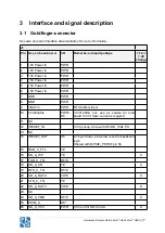
3.1 Goldfinger-connector
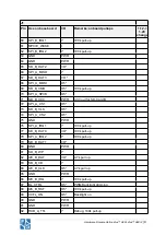
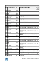
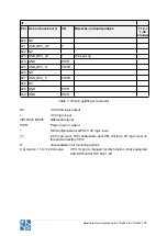
See also efus start interface documentation for more information.
J1
Pin Use on base board
I/O
Remarks; onboard pullups
1.12->
1.20
change
1
+5V Power In
PWR
2
+5V Power In
PWR
3
+5V Power In
PWR
4
+5V Power In
PWR
5
+5V Power In
PWR
6
+5V Power In
PWR
7
GND
PWR
8
GND
PWR
9
VBAT In
PWR
RTC battery input
10
V33-Enable
PWR/
O5
3.3V/100mA out, use as enable for main
board 3.3V if more current is required
11
NC
12
!RESET_IN
I
3.3V pull-up, drive with OC/OD, 100k PU
13
NC
14
!RESET_OUT
O5
4.7k pull down, active low reset for baseboard
logic
Shared with MPCIE_PERST pin 59
15
RXD_C_TTL
I*#
16
SD_A_WP
I*#
X
17
TXD_C_TTL
O5*#
18
SD_A_CD
I*#
X
19
RTS_C_TTL
O5*#
20
SD_A_DAT2
I/O*#
X
21
CTS_C_TTL
I*#
22
SD_A_DAT3
I/O*#
X
23
NC
24
SD_A_CMD
O5*#
X
25
PWM_A
O5*
26
SD_A_VCC
PWR
3.3V out for SD-Card A
X

