background image

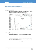
Connectors, LEDs, and Jumpers 

110120-1000A 

31 

J2:  CompactFlash 

Board connector:  Type I and II CompactFlash card socket, Molex 55359-5029 

Mating connector:  CompactFlash card 

The 50-pin CompactFlash socket J2 conforms to the CompactFlash standard for Type I 

and II cards operating at 3.3 V.  Header shields are tied to chassis ground.  For a 

description of the external memory interfaces available on the GCM, see 

External 

Memory

, page 

13

. 

J3:  Ethernet 

Board connector:  RJ-45 socket, Pulse J0026D21BNL 

Mating connector:  RJ-45 plug, CAT5E cable 

Socket J3 is a RJ-45 type with integrated magnetics and indicators that provides a 

10/100 BT Ethernet port.  Shields are tied to chassis ground.  For further details, see 

Ethernet

, pag

17

. 

J4:  USB Host 1 and USB Host 2 (optional) 

Board connector:  USB Type A receptacle, Tyco Electronics 292303-1 

Mating connector:  USB Type A plug 

Socket J4 provides the signals for a USB 1.1 host port.  As a volume production option, 

J4 can be populated with a dual socket providing a second USB 1.1 host port.  Shields 

are tied to chassis ground.  For further details, se

USB Ports

, pag

14

. 

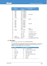
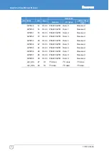
Pin 

Name 

Type 

Description 

A1 

USB_HOST2_PWR 

PO 

5 V DC power output (optional) 

A2 

USB_HOST2- 

IO 

USB Host 2 (optional) 

A3 

US 

A4 

GND 

ground (optional) 

B1 

USB_HOST1_PWR 

PO 

5 V DC power output  

B2 

USB_HOST1- 

IO 

USB Host 1 

B3 

US 

B4 

GND 

ground 

Summary of Contents for PXA320

Page 1: ...Rev A July 2009 DIGITAL TECHNOLOGIES FOR A BETTER WORLD www eurotech com USER MANUAL Graphics ClientM PXA320 Single Board Computer ...

Page 2: ...ty for any error that may appear in this document Trademarks All product or service names are the property of their respective owners Revision History Issue no PWB Date Comments 1 Jul 2008 Preliminary release 2 Feb 2009 Second preliminary release Style and formatting updates Hardware and System Specifications added Revision 4 updates A Jul 2009 Initial release Rev A updates 2008 Eurotech Inc For c...

Page 3: ... USB Disk Drive 13 Communications 14 USB Ports 14 Serial Ports 16 Ethernet 17 SD MMC Interface 17 CAN 2 0B Bus 18 1 Wire Bus 18 I2 C Bus 18 User Interface and Display 19 Display 19 VEE Adapter 19 Backlight 20 Touch Panel 20 Audio Interface 20 Camera Sensor Interface optional 21 Inputs and Outputs 22 General Purpose Inputs and Outputs 22 ADSmartIO 22 Digital I O 23 A D Inputs 23 Keypad Scan 23 Powe...

Page 4: ...aker Left Channel 39 J18 Headphone Out and Audio Line In 40 J19 Stereo Speaker Right Channel 40 J21 GPIO I2C and CSI optional 41 J22 GPIO Serial 1 EIA 422 485 and Reset 43 J23 CAN 2 0B Bus 44 J99 In System Programming 45 J100 Audio Line In Mono 45 System Specification 46 Power Supply 46 Power Supply 46 Power Consumption 46 Electrical 47 PXA320 Processor 47 CPLD 48 Reset and Wake Up Inputs 49 Displ...

Page 5: ...ded system integrators and software application developers Design details apply to the revision listed in Appendix C Board Revision page 57 Block Diagram The following diagram illustrates the system organization of the GCM The functionalities shown with dotted lines or labelled as optional are available as volume production options The following sections provide further details about these various...

Page 6: ...l time clock External memory support CompactFlash Type I and II 3 3 V USB disk drive SD MMC card Communications USB support One USB 1 1 host port and one USB 1 1 client port Optional second USB 1 1 host port and optional USB 2 0 client port For further details see USB Ports page 14 Three serial ports Serial 1 9 wire EIA 232 or optional EIA 422 485 Serial 2 5 wire EIA 232 or optional 3 3 V with IrD...

Page 7: ...rther details see Camera Sensor Interface page 20 Audio Interface AC 97 codec Audio line in Headphone output Stereo speaker output Inputs and Outputs Nineteen ADSmartIO ports Digital inputs and outputs Up to eight A D inputs Up to a 8x8 keypad Up to twenty seven general purpose digital inputs and outputs Power Supply 6 15 V main power input Optional 5 V power input Optional independent backlight p...

Page 8: ...gard to the European Community Electromagnetic Compatibility EMC regulations Because Eurotech supplies only the single board computer and not fully integrated systems Eurotech cannot provide meaningful system level emissions test results It is the responsibility of the user to ensure that systems using the GCM are compliant with the appropriate EMC standards RoHS Compliance The European RoHS Direc...

Page 9: ...vention Explanation GND digital ground plane active low signal positive signal in differential pair negative signal in differential pair The following table describes the abbreviations for direction and electrical characteristics of a signal used in this document Type Explanation I signal is an input to the system O signal is an output from the system IO signal may be input or output P power and g...

Page 10: ...Graphics ClientM User Manual 110120 1000A 10 Software Specification Operating System Support The GCM is compatible with the following operating systems Windows CE Linux ...

Page 11: ...ors up to 3 megapixels PXA320 GPIO Cross Reference The PXA320 general purpose input and output lines GPIOn control various discrete I O on the GCM such as interrupts enables and controls The following table lists the signals that are specific to the GCM GPIO Name Type Description 0 GPIO1_8V_0 O LED D3 control 1 GPIO1_8V_1 O LED D4 control 13 TS_IRQ I 5 wire touch screen interrupt optional 14 USB2D...

Page 12: ...onnection 108 SD1_CD I SD MMC 1 Card Detect 113 117 GPIO113 117 IO GPIO 118 MIC_LINE O Microphone power enable 119 AUDIO_ON O AC 97 codec power control 120 AUDIOPA_ON O Speaker power amplifier shutdown control 121 125 GPIO121 125 IO GPIO 126 BL_ON O Backlight on and off control 127 LCD_ON O Display power control and display data buffer enable 4_2 GPIO4_2 IO GPIO 5_2 VEE_ON O VEE adapter on and off...

Page 13: ...C bus For details about the I 2 C bus see I2C Bus page 18 External Memory Three types of external memory interfaces provide mass storage options for the GCM a CompactFlash socket two SD MMC sockets and up to two USB host ports This section describes the three options CompactFlash Card CompactFlash cards provide removable storage in a wide variety of capacities The GCM supports Type I and II 3 3 V ...

Page 14: ...ts include power switches and transient voltage suppressors The PXA320 controls the power switch enables The GCM supplies 5 V power to the USB host ports through the power switch with over current detection The USB protocol allows client devices to negotiate the power they need from 100 mA to 500 mA in 100 mA increments Make sure to account for power used through USB in your power budget USB mouse...

Page 15: ... option only two GPIOs are available for application use on socket J21 The following diagram illustrates the first volume production option Graphics ClientM PXA320 Processor J12 USB 2 0 UTMI Transceiver USB 2 0 Client J4 USB 1 1 Host 1 USB 1 1 Host 2 2 GPIOs J21 The second option provides a USB 1 1 host port on socket J4 a USB 1 1 client port on socket J12 and a CSI on socket J21 The CSI uses ten ...

Page 16: ...erial 3 page 38 EIA 232 5 wire 3 3V 5 wire Serial 1 interfaces to the PXA320 full function UART supplying the full complement of modem control signals This port is available at EIA 232 levels on header J15 or at EIA422 485 levels on header J22 The processor selects the mode of operation using a control signal mapped to GPIO97 For further details see PXA320 GPIO Cross Reference page 11 Serial 2 int...

Page 17: ... the direction of the signal relative to the GCM Notice that the SD standard references SPI mode signals with respect to the card with pin 2 of the SD header listed as Data In This manual and PXA320 documents reference the signals with respect to the socket In the table pin 2 is listed as Data Out SD Socket Eurotech Name Description Pin Name 4 bit Mode 1 bit Mode SPI Mode 1 DAT3 SD_DAT3 Data 3 IO ...

Page 18: ...rial bus for communications between integrated circuits and for addressing peripherals in a system The bus master addresses devices using the data line and provides a synchronous clock for reading and writing devices Client devices respond only when queried by the master device The GCM uses the PXA320 as the I 2 C bus master to communicate with on board devices In addition connector J21 page 40 in...

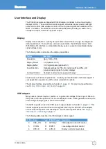
Page 19: ...d PNL_UD up and down signals for active displays Contrast Control Contrast control of some passive displays Features are set at time of production Contact your local Eurotech technical support if your application requires any of the volume production options The display interface is available on header J6 page 32 For electrical specifications see Display VEE Adapter and Backlight page 49 VEE Adapt...

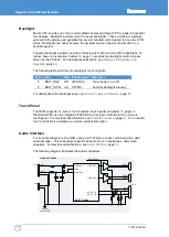
Page 20: ...ption 5 BKLT_ON OD GPIO126 Turns power on or off 6 BKLT_PWM AO PWM0 Controls backlight intensity For details about the backlight power see Power Supply Architecture page 25 Touch Panel The GCM supports a 4 wire or 5 wire resistive touch panel on header J5 page 32 Standard GCMs use the integrated PXA320 touch screen controller to drive a 4 wire touch panel For electrical specifications see PXA320 P...

Page 21: ... supports stereo speakers on header J17 page 39 and header J19 page 40 The audio amplifier drives the differential outputs directly delivering the output power required by stereo speakers Stereo jack J18 page 40 provides a direct connection to stereo headphones The pull down resistors shown in the diagram drain any charge that builds up on the headphone outputs when headphones are not connected Ca...

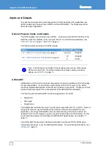
Page 22: ...Ports page 14 ADSmartIO ADSmartIO is a RISC microcontroller programmed to provide additional I O functionality for specialized tasks It can perform a wide variety of functions however the actual functions implemented depend on the firmware loaded on your GCM Contact your local Eurotech technical support for a complete list of the ADSmartIO functionality The following are the ADSmartIO functions su...

Page 23: ...u can create a keypad matrix from a collection of normally open switches When used to scan a keypad the ADSmartIO configures the ROWn lines as inputs with software pull ups enabled and configures the COLn lines as outputs set to 1 logic level high For the scan the keypad scanner sets successive COLn outputs to 0 logic level low then looks for a 0 on one of the ROWn inputs The scanner re reads the ...

Page 24: ...e Other power modes are controlled by the operating system and are typically transparent to the application The operating system is also responsible for adjusting the core voltage for optimal power consumption in each mode In Run mode the power supply is in its standard full power state and applications run normally on the system Specific subsystems may be selectively disabled to conserve power du...

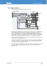
Page 25: ...ng DC power from J1 page 30 generating 3 3 V and 5 V A multi function programmable power management unit provides additional power regulation generating all other voltages required by the on board circuitry For electrical specifications see Power Supply Specification page 46 For systems that supply regulated 5 V power the 5 V step down DC DC controller can be removed as a volume production option ...

Page 26: ...anagement is utilized The following are the subsystems that can be disabled selectively Display Backlight VEE adapter Audio codec Audio amplifier Serial EIA 232 buffers USB ports CompactFlash SD MMC Mechanical The following mechanical drawings specify the dimensions of the GCM as well as locations of key components on the board All dimensions are in inches The first view illustrates the component ...

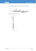
Page 27: ...Hardware Specification 110120 1000A 27 The next diagram illustrates the front view of stereo jack J18 and socket J4 The next diagram illustrates the side view ...

Page 28: ...Graphics ClientM User Manual 110120 1000A 28 The final view illustrates the underside Notice socket J2 is located on the underside ...

Page 29: ... and Indicators This section describes the switches controls and indicators available on the GCM SW1 Reset SW1 is the reset button for the GCM Pressing SW1 shorts the RESET_IN signal to ground issuing a hardware reset to the processor and system peripherals Press this button to restart the GCM without cycling power The RESET_IN signal is also available on J22 page 43 J1 SW1 J8 J13 J16 J14 J21 J11 ...

Page 30: ... the connectors of the GCM Each section provides relevant details about the connector including part numbers mating connectors signal descriptions and references to related sections J1 Power Input Board connector 6 pin header with friction lock 0 1 inch Molex 22 23 2061 Mating connector Molex 22 01 3067 Header J1 accepts input power from an external supply V_IN is the main power input to the GCM O...

Page 31: ...ated magnetics and indicators that provides a 10 100 BT Ethernet port Shields are tied to chassis ground For further details see Ethernet page 17 J4 USB Host 1 and USB Host 2 optional Board connector USB Type A receptacle Tyco Electronics 292303 1 Mating connector USB Type A plug Socket J4 provides the signals for a USB 1 1 host port As a volume production option J4 can be populated with a dual so...

Page 32: ...eader 0 1 inch OUPIIN 3012 34G 00S Mating connector OUPIIN 1001 34G00B1 Header J6 supplies the power control and data signals required to drive a LCD The following table describes the signals included on the header Signal names shown are for TFT active matrix color LCDs at 16 bits per pixel bpp For further details see Display page 19 Pin PXA320 Signal Name Color Active TFT Display at 16 bpp Eurote...

Page 33: ... 30 31 PNL_RL Horizontal mode select 32 PNL_UD Vertical mode select 33 GPIO74 PNL_ENA Panel enable 34 Filtered PWM1 VCON Low voltage contrast control J7 VEE Adapter Board connector 2x4 header 2 mm NSXD MXD2 4PBXX1X An external VEE power supply adapter connects to the GCM on header J7 This header supplies power and control signals to the adapter and receives VEE power from the adapter For further d...

Page 34: ...ff 6 BKLT_PWM AO Backlight intensity 7 GND P ground J9 SD MMC 2 Board connector SD MMC socket 3M SD RSMT 2 MQ Mating connector SD MMC card Socket J9 provides SD MMC 2 for memory and I O expansion Shields are tied to chassis ground A standard GCM supports 3 3 V cards with a volume production option for 1 8 V cards For further details see SD MMC Interface page 17 Pin Name Type Description 1 SD2_DAT3...

Page 35: ...ground 7 SD1_DAT0 IO SD MMC 1 Data 8 SD1_DAT1 IO SD MMC 1 Data 9 SD1_DAT2 IO SD MMC 1 Data 10 SD1_CD I SD MMC 1 Card Detect 11 SD1_WP I SD MMC 1 Write Protect J11 ADSmartIO and 1 Wire Board connector 2x15 shrouded header 2 mm Samtec STMM 115 02 S D SM Mating connector Samtec TCSD series socket ADSmartIO extends the GCM capabilities by providing additional functions inputs and outputs on header J11...

Page 36: ... 14 GND P ground 15 ROW0 I PD0 ADSmartIO ROW1 16 O PD1 17 GND P ground ROW2 18 IO PC2 ADSmartIO 19 ROW3 IO PC3 ROW4 20 IO PC4 21 ROW5 IO PC5 ROW6 22 IO PC6 23 ROW7 IO PC7 UCIO0 24 IO PD5 UCIO1 26 IO PD6 UCIO2 28 IO PD7 25 V3 3 PO 3 3 V power output 27 ONE_WIRE OD 1 Wire bus 29 GND P ground reserved 30 I PD2 ...

Page 37: ...e GPIOs on socket J21 and is mutually exclusive with the CSI option on header J21 For further details about the USB ports and the various options see USB Ports page 14 Pin Name Type Description 1 USB_FCN_CNCT PI DC power input sense connection 2 USB_FCN IO USB Client data 3 USB_FCN 4 nc 5 USB_GND P ground J13 Wakeup Board connector 2 pin header with friction lock 0 1 inch Molex 22 23 2021 Mating c...

Page 38: ...a 3 4 RTS3 O Ready To Send 3 5 TXD3 O Transmit Data 3 6 CTS3 I Clear To Send 3 7 V5 PO 5 V power output 8 nc 9 GND P ground 10 BTEN O 3 3 Bluetooth enable J15 Serial 1 EIA 232 Board connector 2x5 shrouded header 2 mm OUPIIN 3112 10G00DBA Mating connector OUPIIN 1101 series IDC socket Header J15 supplies the PXA320 full function UART signals including hardware flow control at EIA 232 levels For fur...

Page 39: ...in Name Type Description 1 nc 2 nc 3 RXD2 I Receive Data 2 4 RTS2 O Ready To Send 2 5 TXD2 O Transmit Data 2 6 CTS2 I Clear To Send 2 7 V3 3S PO Switched 3 3 V power output 8 nc 9 GND P ground 10 IREN O 3 3 IrDA enable J17 Stereo Speaker Left Channel Board connector 2 pin header with friction lock 0 1 inch Molex 22 23 2021 Mating connector Molex 22 01 3027 The GCM drives a stereo speaker on header...

Page 40: ... the on board audio amplifier An on board pull down forces this signal low supporting stereo headphones only For further details see Audio Interface page 20 Pin Name Pin Type Description 1U HP_L AO Headphone left channel 3U HP_IN Pulled low by on board resistor 4U HP_R AO Headphone right channel 5U AGND P Analog ground AIN_L 1L AI Audio in left channel nc 2L nc 3L AIN_R 4L AI Audio in right channe...

Page 41: ...a Sensor Interface page 20 Note The CSI option and the USB 2 0 client option each use ten of the twelve GPIOs on socket J21 For further details about the volume production options see USB Ports page 14 Pin Name Pin Type Description Standard CSI Option USB 2 0 Client Option 1 V1 8 PO 1 8 V 1 8 V 1 8 V V3 2 PO 3 0 V 3 0 V 3 0 V 3 GPIO4_2 IO 3 3 PXA320 GPIO PXA320 GPIO PXA320 GPIO GPIO100 4 IO 3 3 5 ...

Page 42: ...GPIO Data 2 Reserved GPIO52 18 IO 3 3 PXA320 GPIO Data 3 Reserved GPIO53 20 IO 3 3 PXA320 GPIO Data 4 Reserved GPIO54 22 IO 3 3 PXA320 GPIO Data 5 Reserved GPIO55 24 IO 3 3 PXA320 GPIO Data 6 Reserved GPIO56 26 IO 3 3 PXA320 GPIO Data 7 Reserved GPIO57 28 IO 3 3 PXA320 GPIO Data 8 Reserved GPIO58 30 IO 3 3 PXA320 GPIO Data 9 Reserved I2C_SCL 27 IO I 2 C clock I 2 C clock I 2 C clock I2C_SDA 29 IO ...

Page 43: ...ing a control signal mapped to GPIO97 For further details see Serial Ports page 16 and PXA320 GPIO Cross Reference page 11 Two reset inputs are available on header J22 The RESET_IN signal forces a hardware reset to the processor and system peripherals This signal also connects to the reset button SW1 Reset page 29 For electrical specifications see Reset and Wake Up Inputs page 48 The GPIO_RESET si...

Page 44: ...P ground 25 GPIO121 IO 3 3 PXA320 GPIO 26 GPIO122 27 GPIO123 28 GPIO124 29 GPIO125 30 GND P ground J23 CAN 2 0B Bus Board connector 2 pin header with friction lock 0 1 inch Molex 22 23 2021 Mating connector Molex 22 01 3027 Header J23 supplies a CAN 2 0B bus For further details see CAN 2 0B Bus page 18 Pin Name Type Description 1 CAN IO CAN 2 0B 2 CAN ...

Page 45: ...ion 1 SRST I External Reset 2 TRST I JTAG 3 TMS I 4 GND P 5 TCK I 6 GND P 7 TDI I 8 GND P 9 TDO O 10 GND P 11 nc 12 VREF PO 13 PRG I ATMega ADSmartIO 14 VREF PO 15 MISO O 16 nc 17 MOSI I 18 GND P 19 SCK I 20 GND P J100 Audio Line In Mono Board connector 2 pin header with friction lock 0 1 inch Molex 22 23 2021 Mating connector Molex 22 01 3027 As a volume production option the GCM can provide a co...

Page 46: ...power 3 3 V Notes 1 A backward compatibility package allows the GCM to operate with a 5V only Graphics Client Plus power supply This legacy alternative is available as a volume production option Power Consumption The following table lists typical power consumption for the various power modes of the GCM Symbol Parameter Min Typ Max Units I sleep Sleep mode current note 2 3 4 mA P idle Idle mode pow...

Page 47: ...0 1 Wire interface For a description of this interface see 1 Wire Bus page 18 The integrated PXA320 touch screen controller drives a 4 wire touch panel on header J5 page 32 For a description of this interface see Touch Panel page 20 Symbol Parameter Min Typ Max Units GPIO note 5 VCCIO Input source voltage 3 3 V VIH High level input voltage 0 8VCCIO V VIL Low level input voltage 0 2VCCIO V VOH High...

Page 48: ...0 kHz however the speed is limited to 100 kHz by the RTC chip CPLD A Xilinx XC2C128 CPLD on the GCM provides five GPIOs on header J22 page 43 For a description of the GPIOs see General Purpose Inputs and Outputs page 22 Symbol Parameter Min Typ Max Units GPIO LVCMOS 1 8V note 10 VCCIO Input source voltage 1 8 V VIH High level input voltage note 11 0 65VCCIO VCCIO 0 3 V VIL Low level input voltage ...

Page 49: ...es the display signals The PXA320 LCD controller signals LDD0 through LDD15 as well as the pixel clock vertical sync and horizontal sync are buffered and EMI RFI filtered before reaching header J6 For a description of this interface see Display page 19 Header J8 page 34 supports an external LCD backlight inverter For a description of this interface see Backlight page 20 The GCM also supports an ex...

Page 50: ...e 19 4 7 4 7 kΩ VPNL_UD VPNL_PWR 0 V Backlight VBKLT_PWM PWM control note 20 0 5 0 3 3 0 V_IN V Notes 14 The PXA320 enables the display power and display signal buffer 15 Resistor R121 selects 5 V power while R120 selects 3 3 V 16 Inductor L10 selects 3 3 V signal levels while L11 selects 5 V 17 A standard GCM is configured for 3 3 V display signal voltage levels 5 V displays with VIH 0 6 VPNL_PWR...

Page 51: ...evel output voltage IOH 10 mA VCC 3 0 V 2 2 V VOL Low level output voltage IOL 10 mA VCC 3 0 V 0 5 V RPU Software selectable pull ups to 3 3 V note 23 20 50 kΩ A D Inputs note 22 n Resolution note 24 10 bit RIN Analog input resistance 100 MΩ VREF A D reference voltage 2 5 V VIN A D input voltage range 0 VREF V Notes 21 Row I O column I O UCIO 0 2 RX and TX have series resistance limiting the dc cu...

Page 52: ...ale input voltage 1 Vrms fO Low pass cutoff 16 kHz RIN Input impedance 10 kΩ CIN DC blocking capacitor 1 µF Stereo Headphones note 27 VOUT Full scale output voltage 1 4 Vrms RL External load impedance 32 Ω COUT DC blocking capacitor note 28 330 µF RPD Pull down resistance 1 kΩ Stereo Speakers note 29 RL Speaker load 4 8 Ω POUT Output power THD N 1 RL 4Ω 1 0 2 2 W THD N 10 RL 4Ω 1 0 2 7 W THD N 1 R...

Page 53: ...6 MHz X5 Ethernet 25 000 MHz X6 RTC 32 768 kHz X7 ADSmartIO 7 3728 MHz X8 CAN 2 0B bus 16 000 MHz Real Time Clock The GCM includes a Maxim DS1307 serial real time clock RTC chip to retain the system date and time when the system is powered down This chip includes non volatile RAM that is maintained as long as main or backup power is provided to the chip A long life battery connected to the RTC sup...

Page 54: ...the PXA320 processor www marvell com CompactFlash CompactFlash Association and specification www compactflash org SDIO Card SD Card Association and SDIO specification www sdcard org MMC Card JEDEC MMC 4 0 specification www jedec org USB USB specification and product information www usb org ISO International Organization for Standards ISO and CAN 2 0B specification www iso org iso home htm ...

Page 55: ...control CPLD www xilinx com Atmel Information about the ADSmartIO Controller www atmel com Cirrus Logic Information about the AC 97 codec www cirrus com Maxim Information about the RTC www maxim ic com National Semiconductor Information about the audio amplifier www national com ...

Page 56: ...ird parties and auditing our suppliers and sub contractor s operational activities and arrangements This information is archived within the associated Technical Construction File Eurotech has taken reasonable steps to provide representative and accurate information though may not have conducted destructive testing or chemical analysis on incoming components and materials Additionally packaging use...

Page 57: ... is the board revision Revision History The following is an overview of the revisions to the GCM Revision 2 Pre production Revision 3 Initial release New Features Adds support for 1 8 V SD cards Adds jumper JP1 to JTAG chain Adds capability to control power to J9 and J10 individually Adds support for 128 MB NAND Flash memory at 1 8 V Changes Improves ESD protection Changes real time clock interfac...

Page 58: ...sion A Production release New Features Adds volume production option for backlight power input Adds volume production options for USB ports and CSI Adds additional GPIOs on J21 Adds support for stereo speakers Changes Changes SD MMC 2 from J10 to J9 Changes SD MMC 1 from J9 to J10 Supports USB 2 0 Client at full speed only Changes J21 pinout Changes maximum CPU frequency from 806 MHz to 624 MHz Re...

Page 59: ...0001 DB9 F F null modem cable USB A B cable Operating system of your choice User s Guide this document and operating system guide Please make sure you have received all the components before you begin your development Frequently Asked Questions The following are some of the most commonly asked questions about development kits Q When I plug in power my screen is white and nothing comes up on it A C...

Page 60: ... if I need help developing my application A Eurotech provides technical support to get your development kit running For customers who establish a business relationship with Eurotech we provide support to develop applications and drivers Q Is there online support A Yes Information about the GCM hardware and software is available on the Eurotech support site at www eurotech com Q Can I upgrade the v...

Page 61: ...ope EUROTECH UK tel 44 0 1223 403410 fax 44 0 1223 410457 e mail sales uk eurotech com e mail support uk eurotech com www eurotech com EUROTECH France tel 33 04 72 89 00 90 fax 33 04 78 70 08 24 e mail sales fr eurotech com e mail support fr eurotech com www eurotech com Northern Eastern Europe EUROTECH Finland tel 358 9 477 888 0 fax 358 9 477 888 99 e mail sales fi eurotech com e mail support fi...

Page 62: ...www eurotech com ...
Reviews: