ISPJUNO - Portable ISP Programmer - User Guide V0.84 – 17/04/20
52
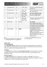
3.2 10-way JTAG header - non-standard pin-out
This connection method is suitable for interfacing the programmer to a Target System which is
programmed via the 'JTAG' interface.
Important note:
This is a non-standard pin-out and so is not directly compatible with any standard JTAG
connector for e.g AVR or ARM devices. A custom wired cable will be required.
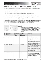
Figure 3.1- Equinox 10-way IDC Header (J7) viewed from above
Warning!
Connecting to the wrong ISP Header may cause
catastrophic damage to the Programmer & Target System
Pin
No
Programmer
Pin name
I/O
Connect to
pin on
Target System
Notes
1
TARGET_VCC
P
TARGET_VCC
Target VCC
This pin should be connected to the
Target System Vcc.
2
BUFFER_ENABLE
IO5
Connect to Clock Buffer
circuit Buffer Enable pin
This pin is used to enable the
output of a remote Clock Buffer.
3
Programmer I/O4
IO4 - O JTAG – TMS
JTAG - Test Mode Select
4
Programmer I/O1
IO1 - I JTAG – TDI
JTAG - Test Data IN
5
RELAY ENABLE
O
Controlled output used to
switch external relay
Direct programmer output with 470
ohm resistor in series. Requires
external transistor to drive relay.
6
Programmer I/O2
IO2 - O JTAG - TDO
JTAG - Test Data OUT
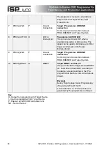
7 + 9 PROG_GND
P
Signal GROUND (0V)
Signal Ground Connection (1)
0V to which the programmer JTAG,
SPI, I2C signal lines are referenced
to.
8
Programmer I/O3
IO3 - O
JTAG - SCK
SPI Clock
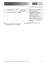
10
PROG_RESET/VPP
O
RESET
Target RESET control pin
This pin controls the Target Device
RESET pin.
Key
O - Output from programmer to Target Device
I - Input to programmer from Target Device
P - Passive e.g. GROUND and power rails
N/C - Not connected


