Page 8
EPSON Research and Development
Vancouver Design Center
S1D13704
Interfacing to the Toshiba MIPS TX3912 Processor
X26A-G-004-02
Issue Date: 01/02/12
2 Direct Connection to the Toshiba TX3912
2.1 General Description
In this example implementation, the S1D13704 occupies the TX3912 PC Card slot #1.
The S1D13704 is easily interfaced to the TX3912 with minimal additional logic. The address bus of
the TX3912 PC Card interface is multiplexed and can be demultiplexed using an advanced CMOS
latch (e.g., 74ACT373). The direct connection approach makes use of the S1D13704 in its “Generic
Interface #2” configuration.
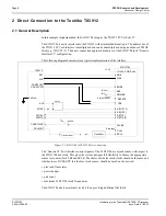
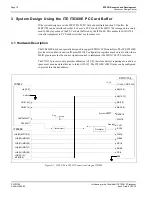
The following diagram demonstrates a typical implementation of the interface.
Figure 2-1: S1D13704 to TX3912 Direct Connection
The “Generic #2” host interface control signals of the S1D13704 are asynchronous with respect to
the S1D13704 bus clock. This gives the system designer full flexibility to choose the appropriate
source (or sources) for CLKI and BCLK. The choice of whether both clocks should be the same, and
whether to use DCLKOUT (divided) as clock source, should be based on the desired:
• pixel and frame rates.
• power budget.
• part count.
• maximum S1D13704 clock frequencies.
The S1D13704 also has internal clock dividers providing additional flexibility.
WE#
RD#
DB[7:0]
WAIT#
BCLK
S1D13704
RESET#
AB[15:13]
D[31:24]
CARD1WAIT*
A[12:0]
TX3912
pull-up
Oscillator
BHE#
CARD1CSL*
CARD1CSH*
Latch
ALE
System RESET
WE*
RD*
BS#
RD/WR#
IO V
DD
IO V
DD
ENDIAN
DB[15:8]
D[23:16]
AB[12:0]
V
DD
DCLKOUT
...or...
CS#
CLKI
See text
Clock divider
IO V
DD
, CORE V
DD
+3.3V
*


