background image

1-8-15

T5300TR1

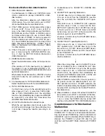
Check Fuse (F601) is blown 
out or not. 
If fuse is blown out, 
do repair method #1

Check whether the primary 
rectifying DC of the Switching 
power supply has an output.
(Reading should be about 168V.

Voltage of the 105V line 
higher than normal?

The transformer of the power 
supply makes a higher sound 
or the oscillation wave form is 
abnormal. 
(E.g. intermittent oscillation)
Connect the positive probe of 
oscilloscope to the pin 16 of 
T601, then connect the negative 
probe to the pin 12. Observe the 
waveform and check to see if 
the waveform is out of limit of 
value shown in Fig.1.

There is no problem on the 
SW power supply

CHECK

#1

#2

#3

#4

Repair method

NO

NO

NO

YES

YES

YES

YES

NO

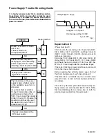
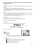
Power Supply Trouble Shooting Guide

It is highly recommended that a variable isolation
transformer which can monitor current be used.
(Alternatively a variable AC source which moni-
tors current will do). Read directions below before
power is added!

Repair method #1

(Power must be off)

Short circuit in the secondary side. check diode D613,
D614, D616, D617 and D618, switching transistor
(Q601), control transistor (Q602), diode and resistor
replace as necessary.

Disconnect 105V diode (D613), 25V diode (D614), 8V
diode (D616), 12V diode (D617), 12V diode (D618)
and Check the load continuity of 105V line, 25V line,
8V line, 12V line through a tester (resistance range).

If the tester indicates a lower resistance value around
0 ohm, the line is short-circuited.

Before repairing the switching power supply, find out
the short-circuited area of such line and repair it.

If the tester does not indicate any low resistance value
(around 0 ohm), no load is short-circuited and there is
no problem.

Check for any defective parts while the secondary rec-
tifying diodes are disconnected (D613, D614, D616,
D617 and D618) perform a diode check in both for-
ward and reverse directions through a tester.

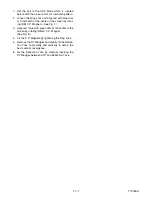
Fig.1

0V

Voltage approx. 5Vp-p

T=Approx. 6 to 14 sec

Oscilloscope setting: 1V/DIV.

                              2 sec./DIV

Summary of Contents for 6319CC

Page 1: ...ustment Procedures I Schematic Diagrams I CBA s Sec 2 Deck Mechanism Section I Standard Maintenance I Alignment for Mechanism I Disassembly Assembly of Mechanism Sec 3 Exploded views and Parts List Section I Exploded views I Parts List 19 COLOR TV VCR COMBINATION SC319C 6319CC EWC1902 ...

Page 2: ...injury to service personnel The possibility exists that improper ser vice methods may damage the equipment It also is important to understand that these CAUTIONS and NOTICES ARE NOT EXHAUSTIVE Funai could not possibly know evaluate and advice the service trade of all conceivable ways in which service might be done or of the possible hazardous consequences of each way Consequently Funai has not und...

Page 3: ... Instructions 1 6 1 Electrical Adjustment Instructions 1 7 1 Block Diagrams 1 8 1 Mechanical Trouble Indicator 1 8 13 Power Supply Trouble Shooting Guide 1 8 15 Schematic Diagrams CBA s and Test Points 1 9 1 Waveforms 1 10 1 Wiring Diagrams 1 11 1 System Control Timing Charts 1 12 1 IC Pin Function Descriptions 1 13 1 Lead Identifications 1 14 1 Sec 1 Main Section I Specifications I Preparation fo...

Page 4: ...10 3 High Voltage kV 25 Description Condition Unit Nominal Limit 1 Misconvergence Center m m 0 4 Corner m m 2 1 Side m m 1 4 2 Tint Control Range deg 30 3 Contrast Control Range dB 6 4 Brightness APL 100 ft L 35 24 5 Color Temperature K 9200 Description Condition Unit Nominal Limit 1 Horizontal Resolution R P Line 230 200 2 Jitter Low R P µS 0 05 0 2 3 S N Chroma AM SP R P dB 38 33 PM SP R P dB 36...

Page 5: ...rop slightly below these specifications Limit specifications represent the abso lute worst condition that still might be considered acceptable In no case should a unit fail to meet limit specifica tions Description Condition Unit Nominal Limit 1 Audio Output Power Max R P W 1 0 0 8 2 Audio S N W LPF R P dB 40 36 3 Audio Distortion W LPF R P 3 0 5 0 4 Audio Freq Response 10dB Ref 1KHz 200Hz R P 8kH...

Page 6: ...ongs tied together and touch the other ohmme ter lead in turn to each tuner antenna input ex posed terminal screw and if applicable to the coaxial connector If the measured resistance is less than 1 0 megohm or greater than 5 2 mego hm an abnormality exists that must be corrected before the instrument is returned to the customer Repeat this test with the instrument AC switch in the off position d ...

Page 7: ...d to the ground side of the AC power source To confirm that the AC power plug is inserted correctly with an AC volt meter measure between the chassis and a known earth ground If a voltage reading in excess of 1 0V is obtained remove and reinsert the AC power plug in the opposite polarity and again measure the voltage potential between the chassis and a known earth ground b Some TV receiver chassis...

Page 8: ...not contact sharp edged or pointed parts H When a power cord has been replaced check that 5 6 kg of force in any direction will not loosen it I Also check areas surrounding repaired locations J Use care that foreign objects screws solder drop lets etc do not remain inside the set K Crimp type wire connector When replacing the power transformer in sets where the connections between the power cord a...

Page 9: ...r cord plug prongs and externally exposed accessible parts RF terminals antenna terminals video and audio input and output terminals microphone jacks earphone jacks etc Measuring Method Power ON Insert load Z between B earth ground power cord plug prongs and exposed accessible parts Use an AC voltmeter to measure across both terminals of load Z See Fig 2 and following table Table 2 Leakage current...

Page 10: ...s The Following Procedures are Recom mended for the Replacement of the Lead less Components Used in this Unit 1 Preparation for replacement a Soldering Iron Use a pencil type soldering iron less than 30 watts b Solder Eutectic solder Tin 63 Lead 37 is recom mended c Soldering time Do not apply heat for more than 4 seconds d Preheating Leadless capacitor must be preheated before installation 130 C ...

Page 11: ...pins of the Flat Pack IC you can remove it easily Fig S 1 3 b Lift each lead of the Flat Pack IC upward one by one using a sharp pin or wire to which solder will not adhere iron wire When heating the pins use a fine tip soldering iron or a hot air Desoldering Machine Fig S 1 4 With Iron Wire a Using desoldering braid remove the solder from all pins of the Flat Pack IC When you use solder flux whic...

Page 12: ...t Pack IC Fig S 1 3 Flat Pack IC Desoldering Braid Soldering Iron Fig S 1 4 Fine Tip Soldering Iron Sharp Pin Fig S 1 5 To Solid Mounting Point Hot Air Blower Iron Wire Soldering Iron or Fig S 1 6 Example Pin 1 of the Flat Pack IC is indicated by a mark Fig S 1 7 Presolder Soldering Iron CBA Flat Pack IC ...

Page 13: ...ded to remove any static electricity that may be charged on the body Ground for Work Bench Be sure to place a conductive sheet or copper plate with proper grounding 1MΩ on the work bench or other surface where the semiconductors are to be placed Because the static electricity charge on the clothing will not escape through the body grounding band be careful to avoid contacting semiconductors to clo...

Page 14: ...ism assembly is removed from the Main CBA due to servicing this switch can not be oper ated automatically Preparing 2 1 To eject the tape press the STOP EJECT button on the unit or Remote Control 2 When you want to record during the Service mode press the Rec button while depressing SW211 REC SAFETY SW on the Main CBA Key Adjustment Mode MENU Picture adjustment mode Press the MENU button to change...

Page 15: ...nnels for viewing or recording You may display the main menu on the TV screen by pressing repeatedly this button on the TV VCR TRACKING function Press to minimize video noise lines or dots on screen during playback mode 6 Remote Sensor Window Receives the infrared signals from the remote control 7 STOP button Press to stop the tape motion EJECT button Press in the Stop mode to remove tape from TV ...

Page 16: ...ess to select desired channels for viewing or recording To select channels from 1 to 9 first press the 0 button and then 1 to 9 100 button When selecting cable channels which are higher than 99 press this button first then press the last two digits To select channel 125 first press the 100 button then press 2 and 5 16 MENU button Press to display the main menu on the TV screen 17 DISPLAY button Di...

Page 17: ... 2 two Screw S 2 5 Refer to the following Reference Notes in the Table Reference Notes in the Table 1 Removal of the Rear Cabinet Remove Screws 4 S 1 Caution Discharge the Anode Lead of the CRT with the CRT Ground Wire before removing the Anode Cap 2 Removal of the Tray Chassis Discharge the Anode Lead of the CRT with the CRT Ground before removing the Anode Cap Disconnect the following Anode Cap ...

Page 18: ...1 6 2 T7300DC Fig 1 ANT S 1 S 1 1 REAR CABINET S 1 S 1 S 1 S 1 Fig 2 ...

Page 19: ...1 6 3 T7300DC S 2 S 4 S 3 S 3 S 4 S 4 S 4 S 4 S 2 S 2 S 2 2 TRAY CHASSIS 4 MAIN CBA 3 DECK UNIT Fig 3 ...

Page 20: ...1 6 4 T7300DC Fig 4 S 5 S 5 S 5 S 5 5 CRT CRT CBA ANODE CAP ...

Page 21: ... CL504A CL501A SCREEN CN501 CN802 CN601 CN571 FOCUS CRT CBA AC CORD CL403 FE HEAD CYLINDER ASSEMBLY AC HEAD ASSEMBLY CAPSTAN MOTOR DECK UNIT MAIN CBA CL401 CL504 CL201 CL402 CL501 CRT ANODE GND TO SPEAKER TO DEGAUSS COIL ...

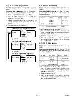
Page 22: ...1 Use the service remote control unit 2 Turn the power on 3 Press WAKE UP SLEEP button on the service remote control unit 1 DC 114V B Adjustment Purpose To obtain correct operation Symptom of Misadjustment The picture is dark and unit does not operate correctly Note J192 B J213 GND VR601 Main CBA 1 Connect the unit to AC Power Outlet 2 Connect DC Volt Meter to J192 B and J213 GND 3 Adjust VR601 so...

Page 23: ...hen display will change H Adj and AGC 5 Press CH o p buttons on the remote control unit so that the display will change 0 to 7 At this moment choose display 0 to 7 when the Frequency counter display is closest to 15 734kHz 300Hz 6 Turn the power off and on again 4 2 C Trap Adjustment Purpose To get minimum leakage of the color signal carrier Symptom of Misadjustment If C Trap Adjustment is incorre...

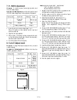
Page 24: ... on the remote control unit so that the monoscope pattern is 90 5 of display size and the circle is round 6 V Shift Adjustment Purpose To obtain correct vertical position of screen image Symptom of Misadjustment If V position is incor rect vertical position of image on the screen may not be properly displayed 1 Enter the Service mode See page 1 4 1 Press 9 button on the remote control unit and sel...

Page 25: ...l line appears on the CRT 4 Press the VOL p button Press VOL p then display will change CUT OFF DRIVE VCO adjustment Analog OSD adjust ment 5 Choose CUT OFF DRIVE Mode then press 1 but ton This adjustment mode is CUT OFF R 6 Press the CH o p button until the horizontal line becomes white 7 Choose CUT OFF DRIVE mode then press 2 but ton This adjustment mode is CUT OFF G Press CH o p until the horiz...

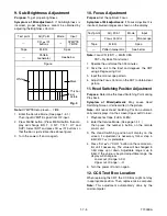
Page 26: ... Point during Play back Symptom of Misadjustment May cause Head Switching Noise or Vertical Jitter in the picture Note Unit reads Head Switching Position automati cally and displays it on the screen Upper Left Corner 1 Playback test tape FL8A FL8N 2 Enter the Service Mode See page 1 4 1 Then press the number 5 button on the remote control unit 3 The Head Switching position will display on the scre...

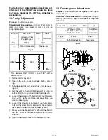
Page 27: ...and adjust the Purity Mag nets so that a red field is obtained at the center of the screen Tighten Ring Lock See Fig 5 6 7 Slowly push the Deflection Yoke toward the bell of the CRT and set it where a uniform red field is obtained 8 Tighten the clamp screw on the Deflection Yoke 14 Convergence Adjustment Purpose To obtain proper convergence of red green and blue beams Symptom of Misadjustment If C...

Page 28: ...y rotat ing RB C P Magnets See Fig 7 3 Align red blue with green dots at the center of the screen by rotating RB G C P Magnet See Fig 8 4 Fix the C P Magnets by tightening the Ring Lock 5 Remove the DY Wedges and slightly tilt the Deflec tion Yoke horizontally and vertically to obtain the best overall convergence 6 Fix the Deflection Yoke by carefully inserting the DY Wedges between CRT and Deflec...

Page 29: ...L RENTAL SPL PLAY 32 REC EE PB REC EE PB 27 EXT H INSEL SP MUTE SP MUTE 12 SW211 REC SAFETY TO VIDEO BLOCK TO AUDIO BLOCK KEY SWITCH KEY SWITCH SW201 SW205 1 8 1 1 8 2 T7300BLS SCL MEMORY SDA 6 5 REC LED 22 REC LED 23 P DOWN 84 P ON H P DOWN P ON H 31 D204 REC AL 5V LD SW 1 I 2 C OPEN 45 71 AL 5V SW212 LD SW CS 7 TO POWER SUPPLY BLOCK SW206 SW210 SDA SCL TO CHROMA TUNER BLOCK SDA SCL IC202 WF3 I 2...

Page 30: ...NAL PROCESS 35 REC VIDEO SIGNAL PB VIDEO SIGNAL MODE SP REC 13 91 90 89 88 42 38 CHARA MIX 6dB AMP ENV DET AGC AMP HPF FROM TO SERVO SYSTEM CONTROL BLOCK TO CHROMA TUNER BLOCK TO CHROMA TUNER BLOCK FROM TO SERVO SYSTEM CONTROL BLOCK CYLINDER ASSEMBLY RF SW RF SW 93 V ENV J190 WF1 J189 PB C MONI BUFFER D V SYNC C SYNC TAPE SPEED SP LP EP ROTA D V SYNC ROTA 34 14 36 16 71 39 59 73 SPL PLAY REC EE PB...

Page 31: ...DIO FROM TO CHROMA TUNER BLOCK J187 A OUT AUDIO HEAD AC HEAD ASSEMBLY A COM A PB REC CL402 AUDIO ERASE HEAD AE H AE H FE H 1 2 FE H FE H GND FULL ERASE HEAD CL403 4 3 1 FE HEAD UNIT LIMITER SERIAL I F FM DET AF AMP SDA SCL CN287 4 3 A COM A PB REC 1 2 AE H AE H FE H FROM TO SERVO SYSTEM CONTROL BLOCK LINE PB TUNER ATT Q302 BUFFER REC AMP 7 98 6 AUTO BIAS 99 LINE AMP MUTE 96 P R ALC 76 80 TUNER LIN...

Page 32: ...ma Tuner Block Diagram SDA SCL TO SERVO SYSTEM CONTROL BLOCK Q301 BUFFER REC VIDEO SIGNAL PB VIDEO SIGNAL Mode SP REC REC AUDIO SIGNAL WF18 WF17 WF10 WF11 J233 B OUT CN303 NO CONNECTION CN303 is used for adjustment at factory INT MONITOR 1 2 SDA 4 SCL 5 I 2 C OPEN I 2 C OPEN 56 CV IN 2 MAIN CBA 34 6 5 19 20 43 24 21 22 23 27 63 64 59 26 14 33 15 16 10 11 31 18 38 41 58 WF2 CHROMA TRAP SERIAL I F I...

Page 33: ... T571 F B T ANODE FOCUS SCREEN MAIN CBA CRT CBA R G B HEATER ANODE GND V501 CRT GND FOCUS SCREEN JK501 HEATER 3 3 CN501 CL501A CL501 REC VIDEO SIGNAL PB VIDEO SIGNAL CN571 P ON 180V 1 1 FROM TO CHROMA TUNER BLOCK 11 S F HV FOCUS VR SCREEN VR FROM CHROMA TUNER BLOCK CL504 1 8 10 1 8 9 B FROM POWER SUPPLY BLOCK 4 3 2 RED GREEN BLUE DEF B H OUTPUT V RAMP NF 1 5 3 4 5 4 3 1 WF12 WF15 WF14 WF16 WF13 RE...

Page 34: ...circuit are not defective before you connect the AC plug to the AC power supply Otherwise it may cause some components in the power supply circuit to fail 4A 125V TIMER 5V P DOWN TO PIN84 OF IC201 P ON ON P ON 5V P ON 5V P ON 8V AL 12V AL 12V AL 5V P SAFETY2 TO PIN3 OF IC201 P ON H FROM PIN31 OF IC201 5V REG 5V REG 5V REG 5V REG 8V REG IC602 Q608 Q611 Q610 Q609 CAUTION FOR CONTINUED PROTECTION AGA...

Page 35: ...s ON 2 POWER SAFETY 2 If P SAFETY 2 port becomes continuously 2 5V or less for 120 msec 4 times 40 msec interval when P ON H port is ON the unit shall be assumed to be the Power Malfunction 2 and immediately turn OFF the POWER MONITOR and switch over the Mechanical Malfunction mode with POWER OFF Shall not unload To return from this mode shall become possible only by POWER Key as in the case of th...

Page 36: ...it keeps the function according to its mode 4 Countermeasure for CASSETTE LOADING Mal function a CASSETTE IN operating Malfunction If LD SW does not go to SB position after a lapse of 5 sec or more from the CASSETTE insertion start the unit starts the CASSETTE OUT opera tion After switch over to CASSETTE OUT operation and then a laps of 5 sec or more from the CAS SETTE OUT operation start if LD SW...

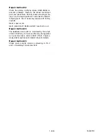
Page 37: ...oni tors current will do Read directions below before power is added Repair method 1 Power must be off Short circuit in the secondary side check diode D613 D614 D616 D617 and D618 switching transistor Q601 control transistor Q602 diode and resistor replace as necessary Disconnect 105V diode D613 25V diode D614 8V diode D616 12V diode D617 12V diode D618 and Check the load continuity of 105V line 2...

Page 38: ... parts then if necessary replace with factory originals R602 is open or not Q601 Q602 D607 D608 and D611 are short or not Repair method 3 The feedback circuit which is monitored by the output of D613 105V may not work and this may be regarded as a possible cause remove IC601 Photo Coupler diode D620 and transistor Q604 check for defects Repair method 4 Check control circuitly which is connecting t...

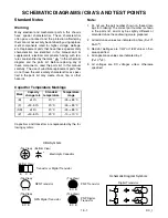
Page 39: ...dentified by the mark in the schematic diagram and the parts list Before replacing any of these components read the parts list in this manual carefully The use of substitute replacement parts that do not have the same safety characteristics as speci fied in the parts list may create shock fire or other hazards Capacitor Temperature Markings Capacitors and transistors are represented by the fol low...

Page 40: ...cement parts which are listed with their part numbers in the parts list section of the service manual 4 Wire Connectors 1 Prefix symbol CN means connector can disconnect and reconnect 2 Prefix symbol CL means wire solder holes of the PCB wire is soldered directly 5 Note Mark is a leadless chip component 6 Mode SP REC 7 Voltage indications for PLAY and REC modes on the schematics are as shown below...

Page 41: ...C4 C5 D1 D2 D3 D4 D5 E1 E2 E3 E4 E5 F1 F2 F3 F4 F5 G1 G2 G3 G4 G5 1 9 3 1 9 4 1 9 5 T7300SCM1 Main 1 4 Schematic Diagram MAIN 1 4 Ref No Position IC201 D 3 IC202 F 4 Q205 C 1 Q206 F 4 J116 D 5 CL201 G 2 CONNECTORS TEST POINTS ICS TRANSISTORS ...

Page 42: ...o Signal REC Audio Signal REC Video Signal 1 9 6 1 9 7 1 9 8 T7300SCM2 Main 2 4 Schematic Diagram MAIN 2 4 Ref No Position IC401 I 2 IC801 M 4 Q401 K 2 Q402 L 4 Q491 L 2 Q871 I 2 Q872 I 2 Q873 I 1 Q874 I 1 Q875 I 1 J187 H 3 J188 L 2 J189 J 4 J190 J 2 CL401 H 4 CL402 H 1 CL403 H 1 CN802 N 4 TEST POINTS CONNECTORS ICS TRANSISTORS ...

Page 43: ...2 U3 U4 U5 T2 PB Audio Signal PB Video Signal REC Audio Signal REC Video Signal 1 9 9 1 9 10 1 9 11 T7300SCM3 Main 3 4 Schematic Diagram MAIN 3 4 Ref No Position IC301 R 2 Q301 R 5 Q302 Q 3 J191 Q 3 J233 T 2 J234 T 2 J239 T 2 J262 T 1 J264 T 1 CN303 U 5 CONNECTORS ICS TRANSISTORS TEST POINTS ...

Page 44: ...A Z 5 CN501 BB 4 CONNECTORS TRANSISTORS MAIN 4 4 Ref No Position IC551 V 5 IC601 Z 2 IC602 X 3 Q571 X 5 Q572 X 5 Q591 X 4 Q601 AA 2 Q602 AA 2 Q604 Z 2 Q605 Y 2 Q606 Y 3 Q607 X 2 Q608 W 2 Q609 X 2 Q610 X 2 Q611 W 1 Q612 W 2 J551 Y 4 J552 Y 4 CL501 Z 5 CL504 Z 5 CN571 W 5 CN601 BB 2 VR601 Z 2 ADJUSTMENT CONNECTORS TEST POINTS ICS TRANSISTORS VOLTAGE CHART Power off mode Ref No S D G Q601 0 0 137 0 1...

Page 45: ...01011 A BHB300F01011 B Sensor CBA Top View END SENSOR BHB300F01011 A BHB300F01011 B CAUTION FOR CONTINUED PROTECTION AGAINST FIRE HAZARD REPLACE ONLY WITH THE SAME TYPE FUSE ATTENTION POUR UNE PROTECTION CONTINUE LES RISQES D INCELE N UTILISER QUE DES FUSIBLE DE MEMO TYPE RISK OF FIRE REPLACE FUSE AS MARKED This symbol means fast operating fuse Ce symbole reprèsente un fusible à fusion rapide 4A 1...

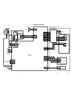
Page 46: ... it may cause some components in the power supply circuit to fail BECAUSE A HOT CHASSIS GROUND IS PRESENT IN THE POWER SUPPLY CIRCUIT AN ISOLATION TRANSFORMER MUST BE USED ALSO IN ORDER TO HAVE THE ABILITY TO INCREASE THE INPUT SLOWLY WHEN TROUBLESHOOTING THIS TYPE POWER SUPPLY CIRCUIT A VARIABLE ISOLATION TRANSFORMER IS REQUIRED WF7 WF9 CAUTION FOR CONTINUED PROTECTION AGAINST FIRE HAZARD REPLACE...

Page 47: ... WF16 Q502 Collector WF15 Q501 Collector WF14 CRT CBA Top View 1 9 21 1 9 22 BT5300F01012 CRT CBA Bottom View CRT CBA Ref No Position Q501 B 2 Q502 B 2 Q503 B 2 CL501A B 2 CL504A B 2 CN501 A 1 TRANSISTORS CONNECTORS ...

Page 48: ... WF10 MAIN 3 4 SCHEMATIC DIAGRAM IC301 PIN 20 WF13 MAIN 4 4 SCHEMATIC DIAGRAM CN571 PIN 5 WF15 CRT SCHEMATIC DIAGRAM Q502 COLLECTOR WF16 CRT SCHEMATIC DIAGRAM Q503 COLLECTOR WF12 MAIN 4 4 SCHEMATIC DIAGRAM Q571 COLLECTOR WF14 CRT SCHEMATIC DIAGRAM Q501 COLLECTOR 0 2 V 0 1 µs 2 V 5 ms 0 2 V 5 V 5 ms 0 5 V 20 µs 0 25 V 20 µs 0 5 V 0 5 V 0 5 ms 1 V 10 ms 0 2 V 0 5 ms 0 5 ms 1 V 20 µs 2 V 5 ms 20 µs 2...

Page 49: ... CL802 1 11 1 T7300WI 1 11 2 CN303 SCL GND SDA INT MONITOR I2C OPEN 1 2 3 4 5 SP 1 SP GND 2 CN287 AUDIO HEAD CONTROL HEAD AC HEAD ASSEMBLY AUDIO ERASE HEAD 4 3 6 5 2 1 FE H 1 FE H GND 2 A PB REC 4 A COM 3 AE H 1 AE H FE H 2 CTL 6 CTL 5 NO CONNECTION CN303 IS USED FOR ADJUSTMENT AT FACTORY P ON 180V P ON 180V GND M LOADING MOTOR CYLINDER ASSEMBLY V R 1 V COM 2 3 V L AL 12V 1 C F R 2 AL 5V 3 D L 12V...

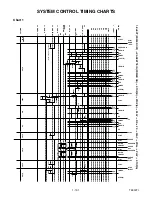
Page 50: ...ILL PLAY LD REV LD FWD LD FWD LD REV LD REV LD REV 0 5S PIN NO CL EJ SB TL SB GC FB GC SS AL SS AU AU TL 1 LD SW CL GC 82 LD CONT M C DRIVE Z ON ON 66 C F R DRUM ROTATION 31 P ON H POWER OFF STOP PLAY RS FS STILL PLAY STOP PLAY 65 A MUTE H 44 D REC L 21 D PB H DISPLAY PAUSE ON PAUSE OFF PAUSE OFF PAUSE ON AU RS AL AU SF AU SF FB SF SF AL AL 0 1S after selecting a channel EJ AL RS SF AU TL FB SS SB...

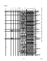
Page 51: ... REV LD REV LD FWD LD REV FF PIN NO SF FB TL AL GC FB GC SS AL SS AU AU TL 1 LD SW CL GC 82 LD CONT M C DRIVE Z ON ON 66 C F R DRUM ROTATION 31 P ON H STOP FF STOP REW STOP REC REC REC PAUSE STOP 65 A MUTE H 44 D REC H 21 D PB H DISPLAY PAUSE REC or PAUSE STOP EJECT STOP EJECT STOP EJECT AU FB FB AU SS GC RS AL AL SF FB TL SB CL EJ RS SS GC AL AU AU AU FB SF SF SF SF SF AU AL AL FB SF EJ AL RS SF ...

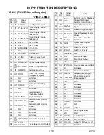
Page 52: ...25 NU Not Used 26 NU Not Used 27 IN OUT REC EE PB YCA IC Mode Output 28 IN OUT TAPE SPEED Tape Speed Control Output 29 OUT EXT H INSEL External Input or Playback SIgnal Output Input Selector Control Signal 30 IN OUT RENTAL Rental Position Control Signal 31 OUT P ON H Power On Signal at High 32 OUT SPL PLAY Special Playback Control Signal 33 IN REC SAFETY Record Protection Tab Detection 34 IN RESET...

Page 53: ...l 79 NU Not Used 80 IN T REEL Take Up Reel Rotation Signal 81 NU Not Used 82 OUT LD CONT Loading Motor Control Signal 83 NU Not Used 84 OUT P DOWN Power Voltage Down Detector Signal 85 NU Not Used 86 NU Not Used 87 IN C FG Capstan Motor Rotation Detection Pulse 88 GND GND AMP 89 IN D FG Drum Motor Rotation Detection Pulse 90 IN D PG Drum Motor Pulse Generator 91 NU Not Used 92 OUT AMP VREF OUT Sta...

Page 54: ...YB11 E Emitter C Collector B Base E C PT204 6B 12 MID 32A22 E C B KRA103M 2SA1346 2SC1815 GR TPE2 2SC3331 T U 2SC2120 O Y TPE2 KTC3203 Y KIA7805API KA7805A AN7805F IN G OUT K E LTV 817 B C F PC817X6 A C M37760M8H8C8GP LA71091M 80 51 81 100 1 30 50 31 2SK2662 48 33 49 M61210FP R60 M61210FP R61 M61210FP R62 32 17 16 1 64 E C B 2SD400 F LA78040A AN5522 IN G OUT 8 5 1 4 LA4224 5 4 8 1 BR24C02F W BR24C...

Page 55: ...1 Service Fixtures and Tools 2 2 1 Mechanical Alignment Procedures 2 3 1 Disassembly Assembly Procedures of Deck Mechanism 2 4 1 Alignment Procedures of Mechanism 2 4 9 Sec 2 Deck Mechanism Section I Standard Maintenance I Alignment for Mechanism I Disassembly Assembly of Mechanism I Alignment Procedures of Mechanism ...

Page 56: ...bove refer to Deck Exploded Views B73 Recording Model only H Hours Check I Change Deck Periodic Service Schedule Ref No Part Name 1 000 H 2 000 H 3 000 H 4 000 H B2 Cylinder Assembly I I B3 Loading Motor Assembly I B8 Pulley Assembly I I B27 Tension Lever Sub Assembly I I B31 AC Head Assembly I B573 B574 Reel S Reel T I B37 Capstan Motor I I B52 Cap Belt I I B73 FE Head I B133 Idler Assembly I I B...

Page 57: ... hard material but since it is very thin avoid cleaning it vertically 2 Wait for the cleaned part to dry thoroughly before operating the unit 3 Do not reuse a stained head cleaning stick or a stained chamois cloth Cleaning of Audio Control Head Clean the head with a cotton swab Procedure 1 Remove the top cabinet 2 Dip the cotton swab in 90 isopropyl alcohol and clean the audio control head Be care...

Page 58: ...J 1 2 Alignment Tape FL8N 2Head only FL8NW 4Head only Azimuth and X Value Adjustment of Audio Control Head Adjustment of Envelope Waveform J 2 Guide Roller Adj Screwdriver Available Locally Guide Roller J 3 Mirror FSJ 0004 Tape Transportation Check J 4 Azimuth Adj Screwdriver Available Locally A C Head Height J 5 X Value Adj Screwdriver Available Locally X Value ...

Page 59: ...that the Moving guide preparations are in the Eject Position 4 Turn the LDG Belt in the appropriate direction shown in Fig M1 until the Moving guide prepara tions come to the Eject Position Stop turning when the preparations begin clicking or can not be moved further However the tape will be left wound around the cylinder 5 Turn the LDG Belt in the appropriate direction con tinuously and the casse...

Page 60: ... the X value and envelope Not good Do the final tape traveling test to see that the tape runs normally in play mode with out creasing or slacking Completion Not good OK OK OK Not good Not good OK Flowchart of Alignment for tape traveling 1 A 1 A 1 B 1 C 1 C 1 D 1 D 1 B 1 C 1 B 1 C 1 A 1 Tape Interchangeability Alignment Note To do these alignment procedures make sure that the Tracking Control Circ...

Page 61: ...ion of the Audio Control Erase Head Symptom of Misalignment If the Horizontal Position of the Audio Control Erase Head is not properly aligned maximum envelope can not be obtained at the Neutral position of the Tracking Control Circuit 1 Connect the oscilloscope to J189 PB C MONI and J116 CTL on the Main CBA Use J190 RF SW as a trigger 2 Play back the Gray Scale of the Alignment Tape FL8N and conf...

Page 62: ...height of Guide Roller 2 Refer to Fig M3 so that the waveform looks like the one shown in Fig M9 4 If the envelope is as shown in Fig M8 adjust the height of Guide Roller 3 Refer to Fig M3 so that the waveform looks like the one shown in Fig M9 5 When Guide Rollers 2 and 3 Refer to Fig M3 are aligned properly there is no envelope drop either at the beginning or end of track as shown in Fig M9 Note...

Page 63: ...older 3 S 5 8 8 Loading Motor Assembly T DM1 DM7 Desolder LDG Belt 2 S 6 9 9 AC Head Assembly T DM1 DM7 S 7 10 2 Tape Guide Assembly T DM1 DM8 P 2 11 10 Door Opener B T DM1 DM8 L 1 L 2 12 11 Pinch Arm B T DM1 DM8 P 3 13 12 Pinch Arm A Assembly T DM1 DM8 14 14 FE Head T DM1 DM9 S 8 15 15 Prism T DM1 DM9 S 9 16 2 Slider Shaft T DM10 S 10 L 3 17 16 C Drive Lever L T DM10 18 16 C Drive Lever R T DM10 ...

Page 64: ...L 2 7 Adjustment Information for Installation Refer to Deck Exploded Views for lubrication 33 2 25 M Brake T Assembly T DM1 DM16 P 6 34 2 25 M Brake S Assembly T DM1 DM16 P 7 35 34 Tension Lever Sub Assembly T DM1 DM16 36 35 T Lever Holder T DM1 DM16 L 6 37 33 M Gear T DM1 DM16 C 6 38 2 15 Sensor Gear T DM1 DM16 C 7 39 33 Reel T T DM1 DM16 40 35 Reel S T DM1 DM16 41 31 35 Moving Guide S Preparatio...

Page 65: ...2 4 3 U25NDA 14 13 11 10 12 7 46 8 29 40 38 37 39 42 41 43 9 33 15 35 36 34 Fig DM1 Top View Fig DM2 Bottom View 31 19 32 24 25 27 26 23 28 21 30 20 22 ...

Page 66: ...rst while pushing the locking tab as shown in the right slide and pull up the right side on 2 to release Pin A and Pin B from the slots A Then remove Pin C and Pin D on 2 from the slots B as shown 1 2 A Fig DM4 3 4 5 6 S 3 S 2 S 4 P 1 Fig DM5 7 46 L 8 A View for A S 5 Fig DM6 Desolder from bottom Lead with Blue Stripe ...

Page 67: ...of 12 are in the grooves of 28 as shown 11 13 12 A 10 L 1 P 3 Adj Screw P 2 L 2 View for A Fig DM8 14 15 S 9 S 8 Fig DM9 17 16 18 S 10 L 3 After removing the Screw S 10 while pressing the Locking Tab L 3 remove 16 Fig DM10 8 8 9 S 7 S 6 LDG Belt A View for A Fig DM7 Desolder from bottom Lead with White Stripe ...

Page 68: ...2 4 6 U25NDA 19 S 11 Cap Belt Fig DM11 20 C 1 A 21 Portions A Portions A View for A Portions A on 21 must be set in the slot on 20 as shown Fig DM12 ...

Page 69: ...Pin of 30 Position of Mode Lever when installed Pin of 34 Fig DM14 23 P 4 C 3 P 4 28 28 23 When installing 23 install the spring P 4 to 28 as shown in the left figure and then install 23 while pressing the spring P 4 to the direction of the arrow in the left figure and confirming that the position of the spring P 4 is placed as shown in the left figure Pin on bottom of 23 Pin on 22 Position of pin...

Page 70: ...2 4 8 U25NDA 32 30 29 L 5 P 5 31 Refer to the Alignment Section Page 2 4 9 Fig DM15 L 6 P 7 P 6 C 6 34 40 37 35 39 33 36 turn turn turn 38 C 7 Fig DM16 41 42 43 L 7 Fig DM17 45 44 Slide Fig DM18 ...

Page 71: ...o the mechanical or electrical parts Alignment points in Eject Position Alignment 1 Loading Arm S and T Assembly Install Loading Arm S and T Assembly so that their triangle marks point to each other as shown in Fig AL2 Alignment 2 Mode Gear Keeping the two triangles pointing at each other install the Loading Arm T Assembly so that the last tooth of the gear meets the most inside teeth of the Mode ...

Page 72: ...ly Install the Rack Assembly so that the first tooth on the gear of the Rack Assembly meets the first groove on the Cam Gear A as shown in Fig AL4 Cam Gear A First tooth First groove on the Cam Gear A Alignment 3 Top View Gear on Rack Assembly Fig AL4 ...

Page 73: ...9C 6319CC EWC1902 TABLE OF CONTENTS Cabinet Exploded Views 3 1 1 Packing Exploded Views 3 1 3 Deck Exploded Views 3 1 4 Mechanical Parts List 3 2 1 Electrical Parts List 3 3 1 Deck Parts List 3 4 1 Sec 3 Exploded views and Parts List Section I Exploded views I Parts List ...

Page 74: ...ectrical Parts List for parts with this mark V501 3 V501 2 L1 L1 L1 L1 B5 B5 A3 A2 A1 1 A1 4 A1 2 A1X A1 3 A1 6 A1 5 B2 B2 B2 B2 B1 B4 B4 A4 L4 L4 B11 CL802 SP801 TL15 TL1 TL1 TL1 TL1 TB26 TB9 1B1 TL2 TL14 TL13 TL2 TL2 TL14 TB3 TB1 TB23 TB10 TB21 TB7 B3 TB2 TL3 TL3 CRT CBA MAIN CBA W601 SCOTCH TAPE 880 SCOTCH TAPE 880 V501 DG601 L551 CLN551 TL17 TL16 TL17 TL17 ...

Page 75: ...Packing X 1 S 1 S 4 S 3 S 3 S 2 TAPE TAPE X 4 X 3 X 2 X 7 S 6 S 14 FRONT 3 1 3 T7300PEX ...

Page 76: ...ription Part No SLIDUS OIL 150 0VZZ00226 B2 B35 B553 B410 B411 B494 B567 L1053 B74 B10 L1191 B73 B9 B12 B492 B11 B571 B37 B126 L1466 B501 B8 B121 B426 B560 L1450 L1051 L1467 Floil G 374G 0VZZ00109 Blue grease Chassis Assembly Top View Lubricating Point Chassis Assembly Bottom View Lubricating Point L1468 ...

Page 77: ...loil G 374G 0VZZ00109 Blue grease Bottom Side Grease point Bottom Side Grease point View for A Grease point B516 B559 A B52 B507 B488 B551 B133 B568 B569 B513 B502 B570 B491 B565 B417 L1151 B525 B522 B31 L1406 B148 B521 B520 B416 B518 B564 B585 B487 B573 B574 B499 B27 B508 B414 B505 B572 B558 B557 B3 ...

Page 78: ...61 L1341 L1341 L1321 B347 L1321 Note There are two different but interchangeable types of CLEANER LEVER B359 in this model and have different combination with B361 Please see Table 1 for details and combination Refer to DECK PARTS LIST section on page 3 4 1 B361 B359 CLEANER LEVER Type ID No ID No A 0VM411114 Not used 0VM304413 0VM305090 B Table 1 B359 and B361 Combination B361 B359 B529 B360 Type...

Page 79: ...PEAKER S08F02B or DSD0808XQ010 SPEAKER J F097 C5 DSD0808DCP01 TB1 TRAY CHASSIS T5300UA 0EM000588 TB2 TOP SHIELD T5300UA 0EM301573 TB10 RCA HOLDER T5300UA 0EM406869 TB22 19V CHASSIS NO LABEL TJ T7300UA 0EM406881 TB23 TRAY COVER TD250UA 0EM406459 TL1 SCREW P TIGHT 3X12 WASHER HEAD GCMP3120 TL3 SCREW S TIGHT 3X4 BIND HEAD GBMS3040 TL13 SCREW B TIGHT M3X8 BIND HEAD GBMB3080 TL14 SCREW B TIGHT M3X8 BIN...

Page 80: ...0W XV10000T4001 V501 3 RUBBER MAGNET 20X10X1 2 XM05000BV001 CRT TYPE F L551 DEFLECTION YOKE LLBY00ZSY008 LLBY00ZSY008 V501 CRT A48LVL095X TCRT190MS011 V501 1 C P MAGNET JH225 014 XM04000BV009 V501 2 WEDGE FT 00110W XV10000T4001 V501 3 RUBBER MAGNET 20X10X1 2 XM05000BV001 CRT TYPE G L551 DEFLECTION YOKE KDY3MDD18X LLBY00ZMS019 V501 CRT A48LVL095X TCRT190MS011 V501 1 C P MAGNET JH225 014 XM04000BV00...

Page 81: ...µF 50V M CE1JMASTL220 C240 CHIP CERAMIC CAP MELF W K 560pF 50V CZM1JKB0B561 C241 CHIP CERAMIC CAP MELF Y K 4700pF 16V CZM1CKB0Y472 C242 CHIP CERAMIC CAP MELF Y K 1000pF 35V CZM1GKB0Y102 C243 ELECTROLYTIC CAP 22µF 16V M LL or CE1CMASLL220 ELECTROLYTIC CAP 22µF 16V M LL CE1CMASLH220 C244 CHIP CERAMIC CAP MELF F Z 0 01µF 16V CZM1CZB0F103 C245 ELECTROLYTIC CAP 47µF 25V M or CE1EMASDL470 ELECTROLYTIC C...

Page 82: ...µF 16V CZM1CZB0F103 C446 ELECTROLYTIC CAP 1µF 50V M H7 CE1JMAVSL1R0 C447 CHIP CERAMIC CAP MELF F Z 0 01µF 16V CZM1CZB0F103 C448 CERAMIC CAP AX Y M 0 01µF 16V CCA1CMT0Y103 C449 CHIP CERAMIC CAP F Z 0 1µF 50V or CHD1JZB0F104 Ref No Description Part No CHIP CERAMIC CAP F Z 0 1µF 25V CHD1EZB0F104 C450 CHIP CERAMIC CAP CH J 220pF 50V CHD1JJBCH221 C492 ELECTROLYTIC CAP 1µF 50V M H7 CE1JMAVSL1R0 C510 CER...

Page 83: ...1µF 25V CHD1EZB0F104 C857 ELECTROLYTIC CAP 33µF 10V H7 CE1AMAVSL330 C858 ELECTROLYTIC CAP 4 7µF 50V M H7 CE1JMAVSL4R7 C859 CHIP CERAMIC CAP B K 0 015µF 50V CHD1JKB0B153 C860 CHIP CERAMIC CAP MELF Y K 1000pF 35V CZM1GKB0Y102 Ref No Description Part No C861 CHIP CERAMIC CAP CH J 100pF 50V CHD1JJBCH101 C862 CHIP CERAMIC CAP B K 0 01µF 50V CHD1JKB0B103 C863 ELECTROLYTIC CAP 10µF 25V M H7 CE1EMAVSL100 ...

Page 84: ...04 QDPZERA81004 D618 SCHOTTKY BARRIER DIODE 11EQS04 or QD4Z011EQS04 Ref No Description Part No SCHOTTKY BARRIER DIODE ERA81 004 QDPZERA81004 D619 DIODE FR104 B or NDLZ000FR104 RECTIFIER DIODE 10ELS2 or QDQZ0010ELS2 RECTIFIER DIODE ERA22 02 QDPZ0ERA2202 D620 ZENER DIODE MTZJT 776 8B or QDTB0MTZJ6R8 ZENER DIODE DZ 6 8BSBT265 NDTB0DZ6R8BS D621 SWITCHING DIODE 1SS133 T 77 or QDTZ001SS133 SWITCHING DIO...

Page 85: ...102SA1015 Ref No Description Part No Q491 TRANSISTOR 2SC2785 F or QQSF02SC2785 TRANSISTOR 2SC2785 H or QQSH02SC2785 TRANSISTOR 2SC2785 J or QQSJ02SC2785 TRANSISTOR KTC3199 GR or NQS10KTC3199 TRANSISTOR KTC3198 GR or NQS40KTC3198 TRANSISTOR 2SC1815 GR TPE2 QQS102SC1815 Q571 TRANSISTOR 2SD2627LS FEC YB11 QQZZ02SD2627 Q572 TRANSISTOR 2SC1627Y TPE2 QQSY02SC1627 Q591 TRANSISTOR 2SC2785 F or QQSF02SC278...

Page 86: ...JUMPER D0 6 P5 0 JW5 0T R241 CARBON RES 1 4W J 5 6k Ω or RCX4JATZ0562 Ref No Description Part No CARBON RES 1 6W J 5 6k Ω RCX6JATZ0562 R243 CHIP RES 1608 1 10W J 1k Ω RRXAJB5Z0102 R244 CHIP RES 1608 1 10W J 1M Ω RRXAJB5Z0105 R245 CHIP RES 1608 1 10W J 470 Ω RRXAJB5Z0471 R247 CHIP RES 1608 1 10W J 820 Ω RRXAJB5Z0821 R248 CHIP RES 1608 1 10W J 470 Ω RRXAJB5Z0471 R249 CHIP RES 1608 1 10W J 3 3k Ω RRX...

Page 87: ... 10W J 4 7 Ω RRXAJB5Z04R7 R557 CHIP RES 1608 1 10W J 470 Ω RRXAJB5Z0471 R558 CHIP RES 1608 1 10W J 15k Ω RRXAJB5Z0153 R559 CHIP RES 1608 1 10W J 820 Ω RRXAJB5Z0821 Ref No Description Part No R560 CARBON RES 1 4W J 5 1k Ω or RCX4JATZ0512 CARBON RES 1 6W J 5 1k Ω RCX6JATZ0512 R561 CHIP RES 1608 1 10W J 5 6k Ω RRXAJB5Z0562 R562 CARBON RES 1 4W J 4 7 Ω RCX4JATZ04R7 R563 CARBON RES 1 4W J 4 7 Ω RCX4JAT...

Page 88: ...ZPZ05R6 R649 CARBON RES 1 4W J 68k Ω or RCX4JATZ0683 Ref No Description Part No CARBON RES 1 6W J 68k Ω RCX6JATZ0683 R650 CARBON RES 1 4W J 22 Ω or RCX4JATZ0220 CARBON RES 1 6W J 22 Ω RCX6JATZ0220 R651 CARBON RES 1 4W J 560 Ω or RCX4JATZ0561 CARBON RES 1 6W J 560 Ω RCX6JATZ0561 R652 CARBON RES 1 4W J 560 Ω or RCX4JATZ0561 CARBON RES 1 6W J 560 Ω RCX6JATZ0561 R653 CARBON RES 1 4W J 100 Ω or RCX4JAT...

Page 89: ...01 FUSE HOLDER FH V 03078 XH01Z00DK001 FH602 FUSE HOLDER MSF 015 XH01Z00LY001 FH602 FUSE HOLDER FH V 03078 XH01Z00DK001 Ref No Description Part No JK501 CRT SOCKET ISMS02S JSCC220PK003 JK701 RCA JACK YELLOW MSP 281V4 B or JXRL010LY003 RCA JACK YELLOW AV1 15 3 JXRL010RP013 JK702 RCA JACK WHITE MSP 281V1 B or JXRL010LY005 RCA JACK WHITE AV1 15 4 JXRL010RP014 JK801 EARPHONE JACK MSJ 035 12APC or JYSL...

Page 90: ...R508 CARBON RES 1 4W J 1 5k Ω RCX4JATZ0152 R511 CARBON RES 1 4W J 150k Ω RCX4JATZ0154 R512 CARBON RES 1 4W J 150k Ω RCX4JATZ0154 R513 CARBON RES 1 4W J 150k Ω RCX4JATZ0154 R514 CARBON RES 1 4W J 1 5k Ω RCX4JATZ0152 R516 CHIP RES 1608 1 10W J 15 Ω RRXAJB5Z0150 R517 CARBON RES 1 4W J 560 Ω or RCX4JATZ0561 CARBON RES 1 6W J 560 Ω RCX6JATZ0561 R518 CHIP RES 1608 1 10W J 15 Ω RRXAJB5Z0150 R519 CARBON R...

Page 91: ... B487 BAND BRAKE MK10 0VM304416B B488 MODE LEVER MK11 or 0VM101043 MODE LEVER PB MK11 0VM101112 B491 CAM GEAR A MK11 0VM101044 B492 MODE GEAR MK11 0VM305074 B494 DOOR OPENER B MK11 0VM305072 B499 T LEVER HOLDER MK10 0VM304419 B501 WORM HOLDER MK11 0VM305067 B502 CAM GEAR B MK10 0VM304403 B505 PSCW 625504 MK11 0VM413288 B507 REEL WASHER MK9 5 2 1 0 5 0VM410058 B508 S BRAKE SPRING MK10 0VM411121 B51...

Page 92: ...Printed in Japan 2002 02 20 HO SC319C 6319CC EWC1902 T7300UA 2UC 3UD ...

Reviews: