background image

Installation 

Installation 

User's Manual 


 BAB 

740 


2—3

2.1.3 SODIMM Installation 

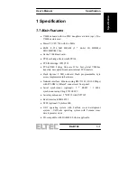
All 144-pin SO-DIMMs up to 64 MByte and some 128 Mbyte SO-
DIMMs that fit into X701 and X702 can be used with the BAB 740. 
The firmware reads the type and size of the SO-DIMM from the SPD 
(Serial Presence Detect) EEPROM installed on the memory module. 
However there are some restrictions and recommendations: 

· 

SDRAMs should be 100 MHz or faster.  

· 

FPMODE or EDO RAMs should be 60 ns or faster.  

· 

X701 must be populated with a memory module.  

· 

If two memory modules are installed they should be of the 
same type but may have different size. Otherwise the 
firmware uses only the module installed in X701.  

· 

Due to performance reasons the use of SDRAM is strongly 
recommended (50% advantage). 

After reset the firmware tests the memory modules. If the test fails or 
the firmware reports the wrong size - the module may not be suitable 
for the BAB 740.  

Summary of Contents for BAB 740

Page 1: ...BAB 740 Basic Automation Board with PowerPC 740 manual Revision 2C...

Page 2: ...Edition Valid for Hardware revision 1A 03 01 2000 AR 2A Valid for Hardware revision 3A 24 04 2001 G M 2B Valid for Hardware revision 3A Valid for Software revision W O9B7 106C I O Address Map changed...

Page 3: ...are performed and what system is used electronic mechanic photocopying recording etc All product and company names are registered trademarks of the respective companies Our General Business Delivery O...

Page 4: ...Consult the dealer or an experienced radio TV technician for help The us of shielded cables for connection of the monitor to the graphics card is required to assure compliance with FCC regulations Cha...

Page 5: ...and adding devices on it carefully read the manuals that came with the package Before using the product make sure all cables are correctly connected and the power cables are not damaged If you detect...

Page 6: ...ycle packaging environmentally friendly Packaging materials are recyclable Please do not dispose packaging into domestic waste but recycle it Please recycle old or redundant devices environmentally fr...

Page 7: ...l 1 2 1 2 2 Flash Memory 1 2 1 2 3 PCI Devices 1 2 1 2 4 VMEbus Interface 1 3 1 2 5 Mechanical 1 3 1 2 6 I O 1 3 1 2 7 Software 1 4 1 2 8 Compatibility 1 4 1 2 9 Related Documents 1 4 2 Installation 2...

Page 8: ...ors 3 2 3 1 4 Parallel I O Connector 3 3 3 1 5 VMEbus Connector P1 3 4 3 2 ADAP 200 Connectors 3 6 3 2 1 8 bit SCSI 3 6 3 2 2 Additional I O 3 7 3 3 CONV 300 Connectors 3 8 3 4 ADAP 740 Connectors 3 9...

Page 9: ...meters 4 1 4 1 Host Bus 4 1 4 2 VMEbus 4 1 4 3 PCI Local Bus 4 4 4 4 Network 4 4 4 5 SCSI 4 5 4 6 Serial I O 4 5 4 7 Keyboard 4 5 4 8 Mouse 4 6 4 9 Parallel I O 4 6 4 10 MTBF Values 4 6 4 11 ESD Value...

Page 10: ...6 2 6 2 1 Entering Boot Parameters 6 2 6 2 2 Printout of Boot Screen 6 2 6 2 3 Ethernet Boot Printout 6 3 7 Appendix 7 1 7 1 Description of On board Devices 7 1 7 1 1 SMI Ticker 7 1 7 1 2 Enhanced Se...

Page 11: ...User s Manual Table of Contents BAB 740 V 7 1 9 PCI IDSEL 7 9 7 2 Factory settable Jumpers 7 9...

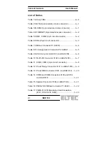
Page 12: ...P1 X2001 3 4 Table 8 Pin Assignment of Connector P2 X2002 3 5 Table 9 SCSI Connector 8 bit X103 on ADAP 200 3 6 Table 10 50 Pin I O Connector X102 on ADAP 200 3 7 Table 11 COM3 COM4 9 pin min D connec...

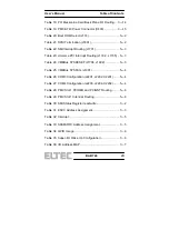
Page 13: ...Table 24 VMEBus SYSRESET J1706 J1902 5 3 Table 25 VMEBus SYSFAIL J1901 5 4 Table 26 COM3 Configuration J2201 J2202 X2201 5 4 Table 27 COM4 Configuration J2203 J2204 X2202 5 4 Table 28 PMC Slot 1 PCIR...

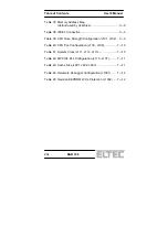
Page 14: ...le 39 CPU Drive Strength Configuration J101 J102 7 9 Table 40 CPU PLL Configuration J103 J106 7 10 Table 41 System Clock J111 J112 J113 7 10 Table 42 MPC106 PLL Configuration J110 J107 7 11 Table 43 C...

Page 15: ...tents BAB 740 IX List of Figures Figure 1 Block Diagram 1 5 Figure 2 Connection Diagram 2 1 Figure 3 Parts Side Jumpers 5 1 Figure 4 Solder Side Jumpers 5 2 Figure 5 PMCE 740 Jumpers 5 5 Figure 6 BAB...

Page 16: ...Table of Contents User s Manual BAB 740 X...

Page 17: ...ansfers decoupled from board internal PCI transfers Flash Eprom 2 MB onboard Flash programmable byte access implemented in hardware Network interface Ethernet using DEC21143 10 100 Mbps with PCI DMA 1...

Page 18: ...44 pin SO DIMM modules 64 bit data bus Memory size can be anywhere between 8 and 128 MB depending on the DIMM modules used Two sockets can be equipped with SO DIMM modules but the board is also runnin...

Page 19: ...bit data transfers in master and slave mode Additionally bus controller arbiter functionality is available Use of the BAB 740 without VMEbus is possible only power must be supplied through VME connec...

Page 20: ...rnet or through the PCI bus BIOS functionality is supplied in the form of the boot program used to start the operating system OS 9 VxWorks It also contains power on self test routines and PCI device a...

Page 21: ...bus SCSI Interface Ethernet Interface IDE Interface Serial 3 4 Serial 1 2 Parallel PS2 Mouse Keyboard Super I O Controller PC97307 PCI PMC Slot 2 Memory SO DIMM Sockets Enhanced Serial Comm Controller...

Page 22: ...Specification Specification User s Manual BAB 740 1 6...

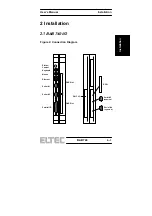
Page 23: ...on User s Manual BAB 740 2 1 2 Installation 2 1 BAB 740 I O Figure 2 Connection Diagram PMC I O PMC Slot PMC Slot Status Control Keyboard Mouse Ethernet SCSI Serial 1 Serial 2 Serial 3 syncron Paralle...

Page 24: ...CE have an internal connection be sure to install resp remove the two board package carefully and simultaneously 2 1 2 What s needed for Installation The BAB 740 must be installed into a 32 bit VMEbus...

Page 25: ...estrictions and recommendations SDRAMs should be 100 MHz or faster FPMODE or EDO RAMs should be 60 ns or faster X701 must be populated with a memory module If two memory modules are installed they sho...

Page 26: ...t panel of the BAB 740 The LEDs have a pulse stretcher to make short pulses visible Table 1 Activity LEDs LED Color Description RUN Green CPU data bus in usage DISK Yellow access to IDE or SCSI bus LN...

Page 27: ...ts before making any connections 3 1 On board Connectors 3 1 1 Keyboard and Mouse Connector Table 2 KEYB 6 pin miniature circular connector Pin Signal 1 KBDATA 2 nc 3 GND 4 5V 5 KBCLK 6 nc 6 2 1 4 3 5...

Page 28: ...onnector Table 4 ETHERNET 8 pin telephone jack connector Front View 1 8 Pin Signal 1 TXD 2 TXD 3 RXD 4 nc 5 nc 6 RXD 7 nc 8 nc 3 1 3 Serial Ports 1 and 2 Connectors Table 5 COM1 COM2 9 pin min D conne...

Page 29: ...Manual BAB 740 3 3 3 1 4 Parallel I O Connector Table 6 PRN 25 pin min D connector Front View Pin Signal 1 STROBE 2 D1 3 D2 4 D3 5 D4 6 D5 7 D6 8 D7 9 D8 10 ACK 11 BUSY 12 PE Paper End 13 SLCT 14 AUT...

Page 30: ...D07 BG2IN D15 9 GND BG2OUT GND 10 SYSCLK BG3IN SYSFAIL 11 GND BG3OUT BERR 12 DS1 BR0 SYSRESET 13 DS0 BR1 LWORD 14 WRITE BR2 AM5 15 GND BR3 A23 16 DTACK AM0 A22 17 GND AM1 A21 18 AS AM2 A20 19 GND AM3...

Page 31: ...G 12 IDEIOCS16 GND MTR0 13 INDEX 5 V DR0 14 DR1 D16 DIR 15 STEP D17 SCSIATN 16 WGATE D18 IDEDB 14 17 IDEDB 15 D19 SCSIBSY 18 SCSIACK D20 SCSIRST 19 SCSIMSG D21 SCSISEL 20 SCSIC D D22 SCSIREQ 21 SCSII...

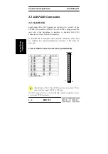
Page 32: ...er end of the SCSI bus J1601 must be installed for signal termination otherwise J1601 must be removed Table 9 SCSI Connector 8 bit X103 on ADAP 200 Pin Description Pin Description 2 DB0 28 GND 4 DB1 3...

Page 33: ...Channel 4 TXD may be changed if a 29 O Serial Channel 4 RTS non standard level 30 I Serial Channel 4 RXD converter board SILC is 31 not connected installed 32 not connected 33 Serial Channel 3 GND2 3...

Page 34: ...View Pin 1 Table 11 COM3 COM4 9 pin min D connector Pin RS232 async Signal default RS232 sync Signal RS422 async Signal RS422 sync Signal 1 DCD DCD CTS RCLK 2 RXD RXD RXD RXD 3 TXD TXD TXD TXD 4 DTR D...

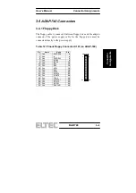
Page 35: ...for the floppy drive must be connected directly to the power supply Table 12 Pinout Floppy Connector X101 on ADAP 740 Pin Name Name Pin 1 Gnd DRVDEN0 2 3 Gnd nc 4 5 Gnd DRVDEN1 6 7 Gnd INDEX 8 9 Gnd M...

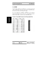
Page 36: ...CD ROM can be connected Cable length should not exceed 40 cm to avoid instable operation EIDE is only available on board versions with EIDE option Table 13 Pinout EIDE Connector X105 on ADAP 740 Pin N...

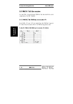
Page 37: ...2 nc nc nc nc 3 RXD RXD RXD RXD 4 RTS TCLK RTS TCLK 5 TXD TXD TXD TXD 6 CTS RCLK CTS RCLK 7 DTR DTR RTS TCLK 8 nc 5V nc 5V RXD RXD 9 GND GND TXD TXD 10 nc nc nc nc Front View 9 10 1 2 The pinout of X1...

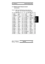
Page 38: ...ed by two PMC Modules 3 5 1 PMCE 740 VMEbus Connector P1 Only GND 5V and 12V are routed from the VMEbus Connector P1 to the Power Connector X403 No VMEbus Signals are used Table 16 PMCE 740 VMEbus Con...

Page 39: ...9 V I O AD 31 20 19 AD 30 AD 29 20 21 AD 28 AD 27 22 21 GND AD 26 22 23 AD 25 GND 24 23 AD 24 3 3V 24 25 GND C BE 3 26 25 IDSEL AD 23 26 27 AD 22 AD 21 28 27 3 3V AD 20 28 29 AD 19 5V 30 29 AD 18 GND...

Page 40: ...P2 33 1 1C 33 17C 34 2 1A 34 17A 35 3 2C 35 18C 36 4 2A 36 18A 37 5 3C 37 19C 38 6 3A 38 19A 39 7 4C 39 20C 40 8 4A 40 20A 41 9 5C 41 21C 42 10 5A 42 21A 43 11 6C 43 22C 44 12 6A 44 22A 45 13 7C 45 23...

Page 41: ...Connector Assignments Connector Assignments User s Manual BAB 740 3 15 3 5 4 PMCE 740 Power Connector Table 19 PMCE 740 Power Connector X403 Pin Description 1 5V out 2 GND 3 GND 4 12V out...

Page 42: ...Connector Assignments User s Manual BAB 740 3 16 Connector Assignments...

Page 43: ...specification ANSI IEEE STD 1014 1987 Rev D1 4 VMEbus Master Slave Capabilities Single cycle A16 A24 A32 A64 D08 EO D16 D32 UAT A40 D08 EO D16 MD32 RMW Master only A16 A24 A32 D08 EO D16 D32 A40 D08 E...

Page 44: ...16 32 64 forever IACK daisy chain driver SYSCLK driver Arbiter Options PRI RRS SGL BBSY filter Requester Options Any one of BR 0 3 RWD ROR ROC Bus ownership timer 16 ms 1024 ms forever Interrupt Handl...

Page 45: ...CI target VME master windows base and size programmable 64 KB to 4 GB window size any of specified address capabilities or user defined Four VME slave PCI initiator windows base and size programmable...

Page 46: ...us CPU to PCI Transfer Options Write post buffer Max 120 MB s peak PCI to Memory Transfer Options Max 120 MB s peak Clock Speed 33 3 MHz IRQs Four PCI interrupts rerouted to selectable ISA interrupts...

Page 47: ...ynchronous transfer 7 MB s synchronous transfer 20 MB s ultra SCSI 4 6 Serial I O 2 Channels PC97307 Full duplex asynchronous 50 b s 115 2 KB s RS232 level 2 Channels Z85230 ESCC Full duplex 50 b s 23...

Page 48: ...ional unbuffered TTL Transfer Rate max 2 MB s 4 10 MTBF Values Includes one 64 Mbyte SODIMM 18900 h computed after MIL HDBK 217E 253270 h realistic value from industry stand experience 4 11 ESD Values...

Page 49: ...4 13 Maximum Operating Humidity 85 relative 4 14 Power Requi ements r Total Power Requirements without PCI extensions 3 8 A max 3 0 A typ 5 VDC 5 100 mA max 30 mA typ 12 VDC 10 100 mA max 10 mA typ 12...

Page 50: ...Board Parameters Board Parameters User s Manual BAB 740 4 8...

Page 51: ...n board Jumpers Figure 3 Parts Side Jumpers X2201 X2202 X701 X702 J1901 J1902 X1301 J2203 J2204 X2001 X2001 J1201 J114 J1302 J1601 J1706 J1301 J1705 J1704 J1703 J1702 J1701 J2201 J2202 X201 X202 X203...

Page 52: ...2 J101 J602 J601 J603 J111 J112 J113 J107 J108 J109 J110 5 1 1 User settable Jumpers Table 20 Boot ROM Select J114 J114 Description open Boot from Boot ROM Short Boot from User ROM default Table 21 SC...

Page 53: ...0 to PCI IRQ A 2 3 route Universe INT1 to PCI IRQ A J1703 Function no Universe INT2 INT3 on PCI 1 2 route Universe INT2 to PCI IRQ B 2 3 route Universe INT3 to PCI IRQ B J1704 Function no Universe INT...

Page 54: ...01 J2201 J2202 X2201 Configuration 1 2 1 2 SILC 200 RS232 async 3 5 5 6 default 6 8 2 4 1 2 SILC 200 RS232 sync 6 8 4 6 6 8 1 2 SILC 300 RS422 async 4 6 2 4 SILC 300 RS422 sync Table 27 COM4 Configura...

Page 55: ...Jumpers Jumpers User s Manual BAB 740 5 5 5 2 PMCE 740 Jumpers Figure 5 PMCE 740 Jumpers SLOT 1 SLOT 0 X403 X201 X101 X203 X102 X103 X202 R101 R102 R103 R104 J201 J202 J204 X402 X401...

Page 56: ...MC Slot 0 3 4 3 4 Use PCIREQ PCIGNT of BAB 740 Onboard SCSI Controller Warning PCIREQ and PCIGNT of PMC Slot 0 or SCSI Controller can only be used if the corresponding device is not equipped Table 29...

Page 57: ...ng SPD of bank2 3 FAILED Activating 64 MByte PowerPC 74x 75x Ver 0008 Rev 3202 at 292 83 MHz PCI devices on local bus No VendorId DeviceId Device Class Sub Class ______________________________________...

Page 58: ...1st level cache OK Setting MPC106 register OK Reading SPD of bank0 1 OK RAM Type SDRAM Reading SPD of bank2 3 FAILED Activating 32 MByte OS 9000 Bootstrap for the PowerPC tm Ethernet 10 Mbit selected...

Page 59: ...his case Select a boot method from the above menu eb Bootp sending bootp request for Address 00 00 5b 00 37 39 Bootp Got Response from server c2 00 00 38 My IP Address will be c2 00 00 b8 My Bootfile...

Page 60: ...Booting Booting User s Manual BAB 740 6 4...

Page 61: ...no need to address these devices with user written code 7 1 1 SMI Ticker The output of counter timer 2 of the W83C553F may be routed to the System Management Interrupt input of the CPU when J1701 is s...

Page 62: ...e Register SMI Status register D7 D6 D5 D4 D3 D2 D1 D0 SMIPE Read SMISR I O Address 808 SMIPE 0 no SMI pending SMIPE 1 SMI pending Write Clears pending SMI Register SMI Status register D7 D6 D5 D4 D3...

Page 63: ...transfer rates up to 3 MBaud synchronous and 230 4 KBaud asynchronous Channel A can be operated with DMA to reduce interrupt load of the CPU for synchronous block protocols DMA channel 0 is used for...

Page 64: ...W83C553 PCI INT A INT B INT C INT D Super I O PC97307 INT 1 3 12 14 15 INT 9 INT 5 PMC 1 ESCC Z85230 RTC MK48T59 PMC 2 SCSI Network VME This diagram shows how the on board interrupt sources are connec...

Page 65: ...NT 7 Parallel Port 7 1 4 SRAM RTC A indirect addressing scheme is used to access the M48T59Y SRAM RTC To access the SRAM RTC the desired address first must be written to I O address 70 and 71 Then the...

Page 66: ...MM ELTEC Revision EEPROM GPIO16 O I2C Clock for SPD of 1st SODIMM ELTEC Revision EEPROM GPIO17 not used GPIO20 not used GPIO21 not used GPIO22 not used GPIO23 not used GPIO24 I HEX Switch LSB GPIO25 I...

Page 67: ...r 081 082 W83C553F DMA Page 087 W83C553F DMA Page 089 08B W83C553F DMA Page 092 W83C553F Port 92 0A0 0A1 W83C553F Interrupt Controller 2 0C0 0DE W83C553F DMA Controller 2 15C PC97307 SuperI O Index 15...

Page 68: ...FFF PCI I O space FE81 0000 FE81 FFFF 0081 0000 0081 FFFF PCI I O space SCSI Controller FE82 0000 FE82 FFFF 0082 0000 0082 FFFF PCI I O space LAN Controller FE83 0000 FEBF FFFF 0083 0000 00BF FFFF PCI...

Page 69: ...M53C860 14 AD 14 21143 15 AD 15 PMC Slot 0 16 AD 16 PMC Slot 1 30 AD 30 Universe II Note that the device numbers differ from Intel convention where number 0 corresponds to AD 11 and number 20 correspo...

Page 70: ...rt short short x 3 40 83 short short x 5 5 25 40 short short x 4 33 66 default short x 5 25 50 short short short x 6 25 40 short x 3 5 40 75 off off SMD jumper for factory use only Note Implementation...

Page 71: ...ault short short x 2 33 50 16 25 short short x 2 5 83 33 short x 2 5 41 50 16 20 short short short x 3 75 100 25 33 short short x 3 50 16 short short short short short short short off SMD jumper for f...

Page 72: ...dware Debugger Configuration J1301 J1301 Operation 1 2 normal operation default 2 3 enable COP Note Implementation specific settings do not change Table 45 Revision EEPROM Write Protection J1302 J1302...

Page 73: ...e Boot configuration ftp bootp Host Configuration Ethernet IP address Development tool revision VxWorks OS 9 Operating system and revision WinNT Error Description What must be done to reproduce the er...

Page 74: ...NOTES...
Reviews: