background image

Chengdu Ebyte Electronic Technology Co.,Ltd.

E32-900M30SA User Manual

Copyright ©2012–2021

Chengdu Ebyte Electronic Technology Co.,Ltd.

7

14

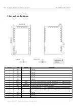
DIO3

Input/Output

General IO port (see SX1276 manual for details)

15

DIO4

Input/Output

General IO port (see SX1276 manual for details)

16

DIO5

Input/Output

General IO port (see SX1276 manual for details)

17

GND

-

Ground

18

GND

-

Ground

19

DIO1

Input/Output

General IO port (see SX1276 manual for details)

20

DIO0

Input/Output

General IO port (see SX1276 manual for details)

21

NRST

Input

Chip reset trigger input pin

22

MISO

Output

SPI data output pin

23

MOSI

Input

SPI data output pin

24

SCLK

Input

SPI data output pin

25

NSS

Input

the module chip selects the pin used to start an SPI communication

26

GND

-

Ground

27

ANT

-

Antenna interface, Sample hole (50

Ω

characteristic impedance)

28

GND

-

Ground

4 Basic operation

4.1 Hardware design

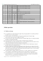
It is recommended to use a DC stabilized power supply. The power supply ripple factor is as small as possible and
the module needs to be reliably grounded;

Please pay attention to the correct connection of the positive and negative poles of the power supply,

reverse connection may cause permanent damage to the module;

Please check the power supply to ensure that between the recommended supply voltage, if exceeding the maximum,
the module will be permanently damaged;

Please check the stability of the power supply. Voltage can not fluctuate greatly and frequently;

When designing the power supply circuit for the module, it is often recommended to reserve more than 30% of the
margin, so the whole machine is beneficial for long-term stable operation;

The module should be as far away as possible from the power supply, transformers, high-frequency wiring and
other parts with large electromagnetic interference;

Bottom Layer High-frequency digital routing, high-frequency analog routing, and power routing must be avoided
under the module. If it is necessary to pass through the module, assume that the module is soldered to the Top Layer,
and the copper is spread on the Top Layer of the module contact part(well grounded), it must be close to the digital
part of the module and routed in the Bottom Layer;

Assuming the module is soldered or placed over the Top Layer, it is wrong to randomly route over the Bottom
Layer or other layers, which will affect the module's spurs and receiving sensitivity to varying degrees;

It is assumed that there are devices with large electromagnetic interference around the module that will greatly
affect the performance. It is recommended to keep them away from the module according to the strength of the
interference. If necessary, appropriate isolation and shielding can be done;

Summary of Contents for E32 Series

Page 1: ...1 E32 900M30S SX1276 868 915MHz SPI SMD Wireless Module...

Page 2: ...Size and pin definition 6 4 Basic operation 7 4 1 Hardware design 7 4 2 Programming 8 5 Basic application 9 5 1 Hardware design and circuit schematic diagram 9 6 FAQ 9 6 1 Communication range is too s...

Page 3: ...duction use modification or disclosure to third parties of this document or any part thereof without the express permission of EBYTE is strictly prohibited The information contained herein is provided...

Page 4: ...port data transmission rate between 0 018K and 37 5Kbps in LoRaTM mode Support data transmission rate of up to 300kbps in FSK mode Support for multiple modulation mode LoRaTM FSK GFSK MSK GMSK OOK Lar...

Page 5: ...ly increase Due to its advanced LoRaTM modulation technology its anti interference performance and communication distance are far superior to the current FSK and GFSK modulation products This module i...

Page 6: ...5 5 5 5 V ensures output power Communication level V 3 3 Operating temperature 40 85 Industrial grade Operating frequency MHz 850 868 915 931 Power Consump tion TX current mA 650 RX current mA 19 Sle...

Page 7: ...XEN Input RF switch receiving control pin connected to external MCU IO high level effective 7 TXEN Input RF switch receiving control pin connected to external MCU IO high level effective 8 DIO2 Input...

Page 8: ...e recommended supply voltage if exceeding the maximum the module will be permanently damaged Please check the stability of the power supply Voltage can not fluctuate greatly and frequently When design...

Page 9: ...al case which will cause the transmission distance to be greatly weakened 4 2 Programming The core of this module is SX1278 SX1276 PA LNA its driving method is completely equivalent to SX1278 SX1276 t...

Page 10: ...sorb and reflect wireless radio wave so the performance will be poor when testing near ground Sea water has great ability in absorbing wireless radio wave so performance will be poor when testing near...

Page 11: ...electrostatic susceptibility Please ensure the humidity is within limited range some parts are sensitive to humidity Please avoid using modules under too high or too low temperature 6 3 BER Bit Error...

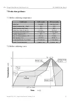
Page 12: ...96 5 Ag3 Cu0 5 Preheat Temperature min Tsmin 100 150 Preheat temperature max Tsmax 150 200 Preheat Time Tsmin to Tsmax ts 60 120 sec 60 120 sec Average ramp up rate Tsmax to Tp 3 second max 3 second m...

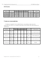
Page 13: ...ommendation The antenna is an important role in the communication process A good antenna can largely improve the communication system Therefore we recommend some antennas for wireless modules with exc...

Page 14: ...cription Issued by 1 0 2021 5 07 Initial version Linson About us Technical support support cdebyte com Documents and RF Setting download link www ebyte com Thank you for using Ebyte products Please co...

Reviews: