background image


Elton User Manual Rev 1.04 

www.diamondsystems.com


Page 15 

4.  FUNCTIONAL BLOCK DIAGRAM 

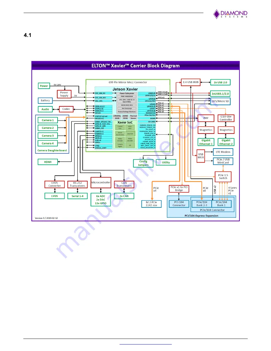
  Elton Baseboard Block Diagram 

The  following  block  diagram  illustrates  the  key  functional  blocks  of  the  Elton  baseboard  with  integrated 
NVIDIA AGX Xavier Series Module and PCI/104 Express 3-Bank Expansion components.  


Figure 4.1-1: Baseboard Functional Block Diagram

Summary of Contents for ELTON ELT-BB01

Page 1: ...08 05 2019 Initial Release 1 02 01 14 2020 Major Feature Updates 1 03 01 26 2020 Added Sections PC 10 DAQ and Getting Started 1 04 03 27 2020 Added Addendum Copyright 2020 Diamond Systems Corporation...

Page 2: ...s 14 4 Functional Block Diagram 15 Elton Baseboard Block Diagram 15 AGX Xavier Series Module Block Diagram 16 5 Mechanical Drawing 17 6 Connector and Jumper Location 18 7 I O Connectors Jumpers and LE...

Page 3: ...s 41 12 Jumper Description 42 Input Voltage Selection JP1 42 Serial Termination and USB Mode Selection JP2 43 Serial Termination Debug UART and PCIe 104 Power JP3 44 13 Getting Started 45 Flashing Ope...

Page 4: ...y impossible to detect because there is no visual sign of failure or damage In this type of damage the board eventually stops functioning because of some defective components Usually the failure can b...

Page 5: ...ssembly operations must be performed when the system is powered off Power Supply Wired Backwards Diamond Systems power supplies and boards are not designed to withstand a reverse power supply connecti...

Page 6: ...Power 9V 20V Wide Input Supply Range 2x2 Samtec IPL1 USB Interfaces 2x USB 2 0 2x5 Header 2x USB 3 1 2x5 Header x2 Ethernet Controllers 10 100 1000 Mbps through I210 Controller with On board Magnetics...

Page 7: ...ties and differ only in feature requirements Model Feature ELT BB01 PCIe 104 ELT BB02 PCIe 104 and PCI 104 ELT BB03 PCIe 104 and PCI 104 X AGX Xavier Modules Overview Measuring L x 3 93 X W 3 42 X H 0...

Page 8: ...SLVS EC Lanes up to 18 4 Gbps Up to 16 Simultaneous Cameras 16x CSI 2 Lanes 40 Gbps in D PHY V1 2 or 64 Gbps in CPHY v1 1 8x SLVS EC Lanes up to 18 4 Gbps Up to 16 Simultaneous Cameras PCIe 5x PCIe G...

Page 9: ...power supply board by mounting the Jumper at location 5 on JP3 This disables the 5V and 3 3V power feed from the Elton baseboard to the PCIe 104 or PCI 104 Cards NOTE The 12V pins on the PCI 104 conn...

Page 10: ...ol is implemented by a Pulse Width Modulation PWM circuit which is located on a separate latching connector To implement a dual channel on the LVDS LCD output the NXP PTN3460 bridge IC must be program...

Page 11: ...the Elton baseboard does not feature a Debug Serial Console Port but provides the ability to set up a Debug Serial Console by mounting the Jumper at location 6 on JP3 This will initiate the Serial Co...

Page 12: ...oller UFSHC A MIPI Unified Protocol UniPro Interface Controller Two MIPI M PHY MPHY High Speed Serial Interfaces The UFS blocks can be operated in single x1 or dual x2 lane configurations to support o...

Page 13: ...port and 1x USB 3 1 ports are connected to 2x5 USB 3 0 header 1x USB 2 0 port is muxed between the NimbeLink LTE module and MiniCard socket via Mux By default it is connected to the NimbeLink LTE modu...

Page 14: ...the left at the baseboard edge The LEDs are displayed on a silkscreen panel with a description of their function and status as listed in the table below Led Indicators Description Power IN Green LED...

Page 15: ...CK DIAGRAM Elton Baseboard Block Diagram The following block diagram illustrates the key functional blocks of the Elton baseboard with integrated NVIDIA AGX Xavier Series Module and PCI 104 Express 3...

Page 16: ...ge 16 AGX Xavier Series Module Block Diagram The following block diagram illustrates a high level view of the AGX Xavier Series components The ports are broken out through the carrier board Figure 4 2...

Page 17: ...Elton User Manual Rev 1 04 www diamondsystems com Page 17 5 MECHANICAL DRAWING Figure 5 1 illustrates the mechanical top view of the Elton baseboard Figure 5 1 Elton Baseboard Mechanical Top View...

Page 18: ...ms com Page 18 6 CONNECTOR AND JUMPER LOCATION Figure 6 1 displays the top and bottom layout views of the Elton baseboard A description of the Jumpers and Connectors is tabulated below Figure 6 1 Base...

Page 19: ...04 www diamondsystems com Page 19 Figure 6 2 displays the bottom layout view of the Elton baseboard A description of the Jumpers and Connectors is tabulated below Figure 6 2 Baseboard Jumper and Conne...

Page 20: ...Power Disable J4 Backlight LED Block J5 CAN1 1st LED Marked in Figure 6 1 Power IN J6 CAN2 2nd LED Power ON J7 LVDS 3rd LED HOST LED J8 Battery 4th LED SAM User LED J9 M 2 KEY PCIe 5th LED LED1 for ET...

Page 21: ...2x2 Samtec IPL1 Mating Cable Part Number 6981507 RTC Battery Connector J8 The RTC Real Time Clock battery provides power and maintains the internal real time clock and calendar functions in the syste...

Page 22: ...Header Mating Cable Part Number for Latching Connector 6980608 Mating Cable Part Number for Pin Header 6981076 HDMI Connector J19 The baseboard integrates a High Definition Multimedia Interface HDMI...

Page 23: ...ven D1 Odd 17 18 D1 Even D2 Odd 19 20 D2 Even D2 Odd 21 22 D2 Even D3 Odd 23 24 D3 Even D3 Odd 25 26 D3 Even Ground 27 28 Ground DDC CLK 29 30 DDC DATA Connector Number Type TFM 115 02 L DH Side Entry...

Page 24: ...pe 2mm Dual Row Right Angle Pin Header Mating Cable Part Number for Latching Connector 6980602 Mating Cable Part Number for Pin Header 6981082 PCIe 104 Connector J1 The PCIe 104 connector is implement...

Page 25: ...GND AD06 5 GND AD09 AD08 GND 6 AD11 VI O AD10 M66EN 7 AD14 AD13 GND AD12 8 3 3V C BE1 AD15 3 3V 9 SERR GND SB0 PAR 10 GND PERR 3 3V SDONE 11 STOP 3 3V LOCK GND 12 3 3V TRDY GND DEVSEL 13 FRAME GND IRD...

Page 26: ..._P 49 50 CSI_6_D1_P CSI_4_D1_N 51 52 CSI_6_D1_N GND 53 54 GND DVDD_CAM_LV 55 56 DVDD_CAM_LV DVDD_CAM_LV 57 58 DVDD_CAM_LV CSI_5_D0_P 59 60 CSI_7_D0_P CSI_5_D0_N 61 62 CSI_7_D0_N GND 63 64 GND CSI_5_CL...

Page 27: ...elow RS 232 Interface TX1 A01 B01 RTS1 RX1 A02 B02 CTS1 GND A03 B03 GND TX2 A04 B04 RTS2 RX2 A05 B05 CTS2 RS 422 SP336 Interface TX1 A01 B01 TX1 RX1 A02 B02 RX1 GND A03 B03 GND TX2 A04 B04 TX2 RX2 A05...

Page 28: ...the host The TX signal channels on the socket and the RX signal channels on the AGX Xavier Series Module are bi directional The RX signal on the socket is driven by the TX signal on the installed modu...

Page 29: ...the module installation site is not connected to Ground The pinouts for the connector are specified below GND 1 2 3 3V GND 3 4 3 3V PETn3 5 6 N C PETp3 7 8 N C GND 9 10 LED1 PERn3 11 12 3 3V PERp3 13...

Page 30: ...und The following table provides the signal type and its definition Signal Name Definition AIN 5 0 AIN 2 0 Single Differential Ended Analog Inputs at 3 3V Level DAC 1 0 DAC Outputs at 3 3V Level DIO 1...

Page 31: ...ctor Type 1 25mm Single Row SMD RA Cable Part Number 6981182 UFS Interface Connector J15 The AGX Xavier Series Module supports a x1 lane UFS interface The pinouts for the connector are specified below...

Page 32: ...tch SMT RA 6981182 DAQ FCI 98414 F06 26ULF 2x13 2mm Pitch TH Header RA 6980606 Utility PINREX 220 9203GB01 2x3 2mm Pitch TH Header N A PCIe MiniCard JAE MM60 52B1 E1 R650 52 Pin MiniCard Full Size wit...

Page 33: ...User Manual Rev 1 04 www diamondsystems com Page 33 10 JETSON XAVIER B2B CONNECTOR INTERFACE The following table figure depicts Jetson AGX Xavier Series Module Connector Pin Out Matrix Part 1 Columns...

Page 34: ...Elton User Manual Rev 1 04 www diamondsystems com Page 34 The following table figure depicts Jetson AGX Xavier Series Module Connector Pin Out Matrix Part 2 Columns G L...

Page 35: ...us expansion system implemented by a pair of surface mount connectors in a slot oriented platform that incorporates a non conventional point to point interface technology while still retaining compati...

Page 36: ...he pinouts for the PC 104 connector can be obtained from the PC 104 Signal Assignments site The signals marked J1 P1 are found only on the 8 bit version while J2 P2 are found on the 16 bit version PC...

Page 37: ...Express incorporates Link Shifting functionality which eliminates the need for the PCI slot selection switches Jumpers found on PCI 104 and PC 104 Plus peripherals PCI 104 Express supports PCI Expres...

Page 38: ...ith Type 1 hosts USB 3 0 SATA and LPC peripherals are compatible only with Type 2 hosts The pin assignments on Bank 1 of the connector are identical to Type 1 and Type 2 pin assignments hence all the...

Page 39: ...king Third Party PC 104 Expansion Boards As an open standard PC 104 offers a robust platform on a global level that allows an extensive range of compatible boards processors expansion buses CPUs A V c...

Page 40: ...s a subset of the PCIe 104 3 bank bus compatible with existing PCI 104 Express Type 1 and Type 2 modules The OneBank connector occupies the same slot as Bank 1 of the 3 Bank connector Hence OneBank si...

Page 41: ...Power supply on Power Good Power 3 3V 5V 12V and SMBus Type 1 implements an additional feature one x16 PCI Express Link that can be configured as two x8 Links or two x4 PCI Express Links dependent on...

Page 42: ...s for Low Voltage Differential Signaling Back Light LVDS BKLT Low Voltage Differential Signaling Virtual Device Driver LVDS VDD can be configured It can also be used to set the voltage supplied to VIO...

Page 43: ...the Jumper will set the USB routing to the LTE module which is the default setting or to the PCIe MiniCard The following table shows the pinouts function and termination modes on the JP2 block The tex...

Page 44: ...nable or disable the power supply to the PCIe 104 card The sixth position of the Jumper will select the debug UART or UART1 via serial port 1 on J22 The following table specifies the pinouts functions...

Page 45: ...ational Diamond Systems Image is released as a compressed tar gz file that can be unzipped on a Linux Host Machine and flashed on to the AGX Xavier Series Module To update the image on the AGX Xavier...

Page 46: ...e following command depicted in the Screen below It may take a few minutes for the file to unzip sudo tar pxvf elton release 0 1 20190627 tar gz NOTE The tar gz file name is liable to change according...

Page 47: ...take 15 20 minutes to complete NOTE Do not interrupt or interfere with the USB connectivity or the power supply to Elton until the flashing procedure is complete When the flashing is complete the mod...

Page 48: ...I O connections must be referenced to the analog Ground pins 9 and 10 and all digital I O signals must be referenced to the digital Ground pins 11 and 26 A standard 2x13 2mm pitch ribbon cable connec...

Page 49: ...he I O connector NOTE It is recommended to avoid using digital Ground pins for analog input measurements since it will display a higher noise level and result in less accurate readings In a differenti...

Page 50: ...characteristics of the microcontroller regarding accuracy readings the full input range of 0 3 3V may not be attainable In some scenarios the minimum measurable voltage maybe a few millivolts above 0V...

Page 51: ...higher noise level and will result in poor quality output voltage signals The 12 bit resolution refers to the output of the requested voltage in 12 bit integers with an accuracy of 3 3V 4096 or appro...

Page 52: ...on The circuit provides a LED connection tied to a GPIO line that is fully functional and can be controlled by the software to monitor the circuit Peripheral Control The peripherals listed below are a...

Page 53: ...4 59 PB30 GPIO A5 51 PA27 GPIO A6 50 PB23 GPIO A7 49 PB22 GPIO B0 46 PA25 GPIO B1 45 PA24 GPIO B2 44 PA23 GPIO B3 43 PA22 GPIO B4 17 PA08 5 0V Rail Scale Factor 2 0 18 PA09 Main Input Voltage Scale Fa...

Page 54: ...mum specified TTP temperature controls the temperature range of all components on the baseboard To determine the best method to interface the TTP with the respective Thermal Solution and ensure therma...

Page 55: ...performance and optimize performance while maintaining the baseboard rated temperature The Heat Spreader material is manufactured under high temperature and high pressure sintering of particles to for...

Page 56: ...Inner Mounting Holes on the baseboard and for the AGX Xavier Series Module Thermal Accessory Figure 15 1 2 Schematic Top View Section with Mounting Hole Specifications The following image depicts the...

Page 57: ...i PCIe Full Size Card Utility PWR_BTN RESET FORCE RECOVERY Digital Analog Specifications Number of Lines 13 Direction Programmable Bit by Bit Input voltage Logic 0 0 0V Min 0 99V Max 1uA Logic 1 2 31V...

Page 58: ...e programmed to Power Up by invoking a script session using the following script home nvidia lvds en sh Enter the following command lines in the terminal to run the script cd home nvidia sudo lvds en...

Page 59: ...arameters Command Description i2cset Write data to an i2c device f y Options f forces access to the device if the device is in a busy mode May return an invalid value y disables interactive mode and b...

Page 60: ...ming is complete the PTN3460 chip must be flashed To execute flashing the following sequence must be used where the Default Values must be replaced with the Offset Hex Values as specified in the table...

Page 61: ...r Synchronized 4k cameras from e con SystemsTM can be plugged into the daughterboard connector to support the four 4 lane or six 2 lane cameras The daughterboard connector also supports i2c and contro...

Page 62: ...or 2 Interface the four adaptor boards to the baseboard using the supplied four micro coaxial cables 3 Connect the micro coaxial cable to the adaptor board connector and baseboard connector as depicte...

Page 63: ...This PWM trigger pulses can be implemented internally using the Internal Trigger Mode or externally using the External Trigger Mode 7 Switch SW1 to EXT_TRIG position when providing PWM trigger signal...

Page 64: ...le through the programmable SP336 serial transceiver and implement selected RS232 422 485 protocols via GPIOs The SP336 is an integrated multiprotocol serial transceiver that contains both RS 232 and...

Page 65: ...ransceiver modes Sysfs GPIO Number RS232 RS422 RS485 443 1 1 0 444 0 1 1 CAN Controller Configuration The AGX Xavier Series Module integrate two independent CAN ports channels which support connectivi...

Page 66: ...e shipping document The Customer will prepay the shipment cost of the product to the Diamond Systems Corporation designated site Diamond Systems Corporation will prepay the return shipping cost of the...

Reviews: