background image

12

About the photos used for "descriptions of the DISASSEMBLY" section

•   The direction from which the photographs used herein were photographed is indicated at "Direction of photograph: ***" 

at the left of the respective photographs.

• 

Refer to the table below for a description of the direction in which the photos were taken.

•  Photographs for which no direction is indicated were taken from above the product

.


1.  REMOTE I/O UNIT

(1)  Disconnect the connector wire, then remove the screw..

2.  P.AMP(L) UNIT

(1)  Disconnect the connector wires, then remove the screws.

The viewpoint of each photograph

(Photografy direction)

View from above

Front side

Direction of photograph: B

Direction of photograph: D

Direction of photograph: C

Direction of photograph: A

TOP COVER

REMOTE I/O UNIT

Proceeding :


TOP COVER

P.AMP (L) UNIT

SIDE COVER (L)

Proceeding :


Summary of Contents for PMA-2020AE

Page 1: ...E1K EUT PMA 2020AE P P INTEGRATED AMPLIFIER Ver 2 S0569 1V02DM DG1210 Some illustrations using in this service manual are slightly different from the actual set Please use this service manual with ref...

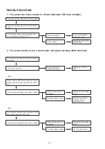
Page 2: ...not be turned on Power indication LED does not light 20 2 The power turned on but a sound does not output normally Both channels 20 3 The power turned on but a sound does output normally Single chann...

Page 3: ...can do with this manual Search for a Ref No phrase Ctrl Shift F You can use the search function in Acrobat Reader to search for a Ref No in schematic diagrams printed wiring board diagrams block diagr...

Page 4: ...ng Adobe Reader 9 On the Document menu click Sign Magnify schematic printed wiring board diagrams 1 Ctrl Space mouse operation Press Ctrl Space on the keyboard and drag the mouse to select the area yo...

Page 5: ...reen Example using Adobe Reader 9 On the Tools menu point to Select Zoom and then click Pan Zoom Window Magnify schematic printed wiring board diagrams 3 Loupe Tool function The Loupe Tool function le...

Page 6: ...ortant safety parts that are indicated by the z mark on schematic diagrams and parts lists be sure to use the designated parts Be sure to mount parts and arrange the wires as they were originally plac...

Page 7: ...RC Composition RS Metal oxide film RW winding RN Metal film RK Metal mixture P Pulse resistant type NL Low noise type NB Non burning type FR Fuse resistor F Lead wire forming 2B 1 8 W 2E 1 4 W 2H 1 2...

Page 8: ...47 k SOURCE DIRECT OFF 135 mV 23 k SOURCE DIRECT ON RIAA Deviation PHONO 20 Hz 20 kHz 0 5 dB Maximum Input PHONO MM 130 mV 1 kHz PHONO MM 10 mV 1 kHz Rated Output PRE OUT 0 9 V Input CD 135 mV n n Ove...

Page 9: ...orm adjustment or parts replacement etc be sure to rearrange them neatly as they were originally bundled or placed afterward Otherwise incorrect arrangement can be a cause of noise generation Wire arr...

Page 10: ...10 Wire arrangement viewed from the bottom Front Panel side Back Panel side...

Page 11: ...TER UNIT and EXPLODED VIEW INPUT UNIT Ref No of EXPLODED VIEW 1 1 PH CD TER UNIT Ref No of EXPLODED VIEW 3 7 BOTTOM COVER Refer to DISASSEMBLY 5 BOTTOM COVER and EXPLODED VIEW DIODE UNIT Ref No of EX...

Page 12: ...ere taken Photographs for which no direction is indicated were taken from above the product 1 REMOTE I O UNIT 1 Disconnect the connector wire then remove the screw 2 P AMP L UNIT 1 Disconnect the conn...

Page 13: ...13 2 Remove the screws 3 Remove the screws then remove the solder...

Page 14: ...14 3 INPUT UNIT and PH CD TER UNIT 1 Disconnect the connector wires 2 Remove the screws TOP COVER INPUT UNIT and PH CD TER UNIT SIDE COVER R Proceeding...

Page 15: ...15 4 P AMP R UNIT 1 Remove the screws 2 Disconnect the connector wires then remove the screws Remove the solder TOP COVER P AMP R UNIT Proceeding...

Page 16: ...onnect the connector wire 2 Remove the screws 3 Remove the screws 4 Loose the Cord holders then disconnect the connector wires TOP COVER FRONT PANEL ASSY SIDE COVER L R Proceeding N0611 Direction of p...

Page 17: ...onnect the connector wire Please refer to EXPLODED VIEW for the disassembly method of each P W B included in PANEL FRONT ASSY 6 BOTTOM COVER 1 Remove the screws TOP COVER BOTTOM COVER SIDE COVER L R P...

Page 18: ...18 7 CE33W 123M 1 Cut the wire clamp bands 2 Remove the screws 3 Remove the screws TOP COVER BOTTOM COVER SIDE COVER L R CE33W 123M Proceeding Direction of photograph D cut...

Page 19: ...IDLING CURRENT Setup 1 Lay the unit at an ordinary position away from a direct current from an air condition or fan Do the adjustment at a temperature between 15 C 59 F and 30 C 86 F 2 Set control as...

Page 20: ...lied to the coil of the standby transformer T101 Check the power amplifier output s offset voltage Check the power amplifier output s offset voltage Power not supplied Offset voltage output is 1V or g...

Page 21: ...rtment Check the voltage of each department Check the operation of the switching relay and speaker relay Check the operation of the switching relay and speaker relay Check the Signal line Check the Si...

Page 22: ...22 BLOCK AND LEVEL DIAGRAM AUX NETWORK...

Page 23: ...23 WIRING DIAGRAM...

Page 24: ...0 JV59 7 5 JV60 7 5 JV61 JV62 17 5 JV63 JV65 JV68 17 5 JV75 25 0 JV76 N0410 20 0 JV80 25 0 JV83 15 0 JV84 22 5 JV85 22 5 JV86 JV87 JV88 12 5 C601 17 5 JV89 C602 C603 C604 C605 C606 R642 C607 R643 C608...

Page 25: ...909 R910 R911 R912 R913 R914 R915 R916 R917 R918 R919 R920 R921 R922 R923 D901 D902 D903 D904 D905 D906 D907 D908 D909 D910 D911 D912 Pri Sec 8U 110132 4 INPUT SEL SW UNIT D951 D952 D953 D954 D955 D95...

Page 26: ...B0371 12 5 JV38 25 0 JV39 Q509 Q511 Q513 N0550 R557 C559 C561 R581 R593 C571 R579 J305 C503 R577 R583 R587 JV10 C545 C547 JV46 15 0 JV5 Z505 R501 R509 R513 R515 R551 J501 1 1 B E B E C B E C B E B E...

Page 27: ...5 JV87 JV88 7 5 JV89 K306 K307 R471 R472 R473 R474 R479 R480 C471 C472 C477 C478 7 5 J301 7 5 J302 N0630 N0640 1 Q904 8U 110133 7 DIODE UNIT B B GND WHT RED BLK BLU YEW B810 B812 B813 B814 C801 C802...

Page 28: ...7 R438 25 0 JV78 R439 R440 R441 R442 R443 22 5 JV83 R444 25 0 JV84 R445 R446 15 0 JV86 R447 17 5 JV87 R448 R449 R450 25 0 JV90 R451 JV91 7 5 R452 JV92 7 5 R453 JV93 R454 7 5 JV94 JV95 12 5 JV96 R457 1...

Page 29: ...904 10K R902 120K C901 0 01 ROTARY SW S901 10 11 12 1 2 3 4 5 6 7 8 9 13 D904 Q902 KRA102S R908 3 9K R911 2 2K Q901 KRA102S 1 8K R922 D956 R907 1 5K R913 100 D902 R910 1 5K 00D2050452017 STYLE PIN Z90...

Page 30: ...EN Z604 DTC114TK Q620 R645 10K J603 SHORT D619 1A3 E J604 SHORT C644 0 22 50 R680 47K R602 0 KRC102S Q630 KRA102S Q631 C647 OPEN D613 KDS160 Q611 KRC102S Q635 2SC4081 6P PH 1 2 3 4 5 6 12P PH N1210 12...

Page 31: ...15 R549 47 1W R517 1 5K AMRS R593 OPEN KTC3423 Y U PH Q514 3 3K AMRR R501 N524 4 Q521 OPEN D512 1SS133 B51 1 R594 OPEN N0550 5P EH IM 1 2 3 4 5 M3_TO P N014 C537 220 50 RFS A R581 V06QB502T 1 2 3 R512...

Page 32: ...1 100P LP K301 6 4 K301 8 5 330K AMRS R301 OPEN C726 J303 OPEN 5 C302 100P LP 3P EH IM N0320 1 2 3 330K AMRS R302 R480 470 N0640 6P EH IM 1 2 3 4 5 6 J302 OPEN R474 1M N0630 6P EH IM 1 2 3 4 5 6 C478...

Page 33: ...A R451 47 1W _AMRA R453 47 1W _AMRA R452 47 1W _AMRA R448 CQ39P FAS C432 CQ39P FAS C431 CQ4700P LP C434 CQ4700P LP C435 CQ4700P LP C436 CQ4700P LP C433 CQ0 01 LP C426 CQ0 01 LP C425 5 6K AMRS R439 5 6...

Page 34: ...7 119 119 71 71 39 40 41 38 11 11 103 31 103 111 101 89 33 10 32 48 43 102 101 50 80 46 46 50 101 101 121 101 101 101 114 110 118 44 117 68 118 118 44 117 118 65 73 67 16 67 21 5 118 73 9 8 58 58 102...

Page 35: ...sp BUSH 4 11 nsp BUSH 1 12 nsp BUSH 1 13 40631008207AD BACK PANEL 1 14 nsp 4P TERMINAL ASSY 2 15 nsp WIRE CLAMPER 22 16 00D4411795007 PLATE T C 1 17 nsp TERMINAL ASS 1 18 nsp PWB BRACKET 2 19 nsp LOCK...

Page 36: ...P 4 117 nsp 3X8 CFTS S Z 4 118 nsp SPECIAL SCREW 16 119 nsp 4X10 CBTS S B 8 120 0RD4770276005 EARTH SCREW 2 121 nsp 3X8 CPS SW W BK 1 WIRE 301 nsp 1P CONT ASSY 1 302 nsp 1P CONT ASSY 1 303 nsp 1P CON...

Page 37: ...No Part No Part Name Remarks Q ty New SEMICONDUCTORS GROUP 201 53121010703AD CARTON CASE 1 202 nsp CABINET SHEET 1 203 53361005412AD CUSHION ASSY 1 204 535510005008D ENVELOPE ZIPPER A4 1 54311021401A...

Page 38: ...N x tal 8MHz 3 XOUT x tal 8MHz 4 TEST I to VSS VDD 5 VDD to VDD 6 P21 XTIN O LED R 7 P22 XTOUT O LED G 8 RESET I reset 9 P20 INT5 STOP I Stop mode cancellation 10 P00 INT0 I ASO protector 11 P01 PDO4...

Page 39: ...e 29 P33 AIN3 AI function A 30 P34 AIN4 STOP2 O muting 31 P35 AIN5 STOP3 O sp output A not use 32 P36 AIN6 STOP4 O NETWORK LED relay drive 33 P37 AIN7 STOP5 I THERMAL DC protector 34 VAREF to VDD 35 A...

Page 40: ...lifier Output 3 TRIN External Trigger Input 4 GND Ground 5 CAP_D Delay Time Capacitor 6 RES_D Delay Time Resister 7 OUT DC Output 8 V Supply Voltage Block Diagram and Sample Application Circuit VCC IN...

Page 41: ...ANK Y 1 Q0619 0620 00D2690088906 DTC114TKT96 C 1 Q0621 00D2690192902 KRC102S RTK P 10K 10K 1 Q0622 00MHX300012AY 2SC4081 Q R 2SC4116 Y GR 1 Q0623 0624 00D2690192902 KRC102S RTK P 10K 10K 1 Q0625 00MHX...

Page 42: ...0 133050078403S CQ93P2D100K FAS 1 C0341 00D2561054001 CF93B1H105K GSG 1 C0342 133050076599S CQ93M2E103J LP 1 C0347 0348 133050074500S CQ93M2E101J LP 1 C0601 00D2544573981 CE04W1H100MT RA3 1 C0602 1330...

Page 43: ...TAPE JP 1 K0303 643810029001S RCA PIN JACK 2P AU MSP 242V3 12 GILT LF 1 K0304 0305 643810028008S RCA PIN JACK 4P AU MSP 244V4 17 GILT LF 1 L0701 0704 00D2359003002 FTZ CHOKE COIL E2 E1C 1 N0210 nsp CO...

Page 44: ...0AD STANDBY TRANS E2 E2 E1C 1 z T0101 10101016600AD STANDBY TRANS JP JP 1 X0601 00MFQ08004061 CSTS MG 8MHZ TAPING 15PF 1 Z0101 nsp M3 SCREW TERMINAL 1 Z0601 nsp STYLE PIN 1 Z0603 nsp STYLE PIN 1 Z0702...

Page 45: ...84907 KRA102S RTK P 10K 10K 1 U0201 00D2630743007 NJM2082DD 1 U0901 00D2623602003 GP1UE271XKVF 1 U0902 00D3991126003 GP1UE261XKVF 1 RESISTORS GROUP z R0227 0228 00MGG0522016X 22 OHM 5 1 6W FLAMERETERD...

Page 46: ...0524 00D2544703719 CE04W1H221MC RFS A 1 C0525 0526 00D2556188005 CQ09S2B103JF PPSC 1 C0527 0528 133050074500S CQ93M2E101J LP 1 C0529 0534 133050076599S CQ93M2E103J LP 1 C0537 0540 00D2544703719 CE04W1...

Page 47: ...1 nsp B12B PH K S LF SN 1 z S0101 66105000300AS POWER SWITCH TV 5 1 S0201 665010010005D 1P PUSH SWITCH 6 2 1 S0251 00D2140127003 RELAY RY 12W 1 S0551 0552 00D2140195006 RELAY FTR F1 1 S0602 6650100100...

Page 48: ...00D2412475904 RD14B2E105JT AMRS 1 R0423 0424 00D2412466926 RD14B2E221JT AMRS 1 R0425 0426 00D2412471940 RD14B2E333JT AMRS 1 R0427 0428 00D2412471982 RD14B2E473JT AMRS 1 z R0429 0432 00D2442695929 RS14...

Page 49: ...50076599S CQ93M2E103J LP 1 C0841 0844 00D2544703748 CE04W1H102MC RFS A 1 OTHERS PARTS GROUP z F0821 0822 00D2061093012 FUSE 25RF 3 15A F006 1 N0250 nsp 2P PLUG B2P3S VH 1 N0260 nsp 2P PLUG B2P3S VH 1...

Page 50: ...50 Personal notes...

Reviews: