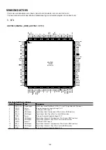
Pin No. Mnemonic
Type
Description
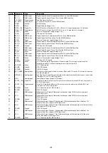
99
PGND
Ground
PVDD Ground.
100
PVDD
Power
PLL Supply Voltage (1.8 V).
101
XTAL
Miscellaneous
analog
Input pin for 28.63636 MHz crystal or an external 1.8 V 28.63636 MHz clock oscillator source to
clock the ADV7623.
102
XTAL1
Miscellaneous
analog
Crystal Output Pin. This pin should be left floating if a clock oscillator is used.
103
PVDD
Power
PLL Supply Voltage (1.8 V).
104
PGND
Ground
PVDD Ground.
105
HP_CTRLA
Digital output
Hot Plug Detect for Port A.
106
5V_DETA
Digital input
5 V Detect Pin for Port A in the HDMI Interface.
107
RTERM
Miscellaneous
analog
This pin sets the internal termination resistance. A 500 Ω resistor between this pin and
ground should be used.
108
DDCA_SDA
Digital I/O
HDCP Slave Serial Data Port A. DDCA_SDA is a 3.3 V input/output that is 5 V tolerant.
109
DDCA_SCL
Digital input
HDCP Slave Serial Clock Port A. DDCA_SCL is a 3.3 V input that is 5 V tolerant.
110
CVDD
Power
Receiver Comparator Supply Voltage (1.8 V).
111
CGND
Ground
TVDD and CVDD Ground.
112
RXA_C−
HDMI input
Digital Input Clock Complement of Port A in the HDMI Interface.
113
RXA_C+
HDMI input
Digital Input Clock True of Port A in the HDMI Interface.
114
TVDD
Power
Receiver Terminator Supply Voltage (3.3 V).
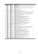
115
RXA_0−
HDMI input
Digital Input Channel 0 Complement of Port A in the HDMI Interface.
116
RXA_0+
HDMI input
Digital Input Channel 0 True of Port A in the HDMI Interface.
117
CGND
Ground
TVDD and CVDD Ground.
118
RXA_1−
HDMI input
Digital Input Channel 1 Complement of Port A in the HDMI Interface.
119
RXA_1+
HDMI input
Digital Input Channel 1 True of Port A in the HDMI Interface.
120
TVDD
Power
Receiver Terminator Supply Voltage (3.3 V).
121
RXA_2−
HDMI input
Digital Input Channel 2 Complement of Port A in the HDMI Interface.
122
RXA_2+
HDMI input
Digital Input Channel 2 True of Port A in the HDMI Interface.
123
HP_CTRLB
Digital output
Hot Plug Detect for Port B.
124
5V_DETB
Digital input
5 V Detect Pin for Port B in the HDMI Interface.
125
DGND
Ground
DVDD Ground.
126
DVDD
Power
Digital Supply Voltage (1.8 V).
127
DDCB_SDA
Digital I/O
HDCP Slave Serial Data Port B. DDCB_SDA is a 3.3 V input/output that is 5 V tolerant.
128
DDCB_SCL
Digital input
HDCP Slave Serial Clock Port B. DDCB_SCL is a 3.3 V input that is 5 V tolerant.
129
CVDD
Power
Receiver Comparator Supply Voltage (1.8 V).
130
CGND
Ground
TVDD and CVDD Ground.
131
RXB_C−
HDMI input
Digital Input Clock Complement of Port B in the HDMI Interface.
132
RXB_C+
HDMI input
Digital Input Clock True of Port B in the HDMI Interface.
133
TVDD
Power
Receiver Terminator Supply Voltage (3.3 V).
134
RXB_0−
HDMI input
Digital Input Channel 0 Complement of Port B in the HDMI Interface.
135
RXB_0+
HDMI input
Digital Input Channel 0 True of Port B in the HDMI Interface.
136
CGND
Ground
TVDD and CVDD Ground.
137
RXB_1−
HDMI input
Digital Input Channel 1 Complement of Port B in the HDMI Interface.
138
RXB_1+
HDMI input
Digital Input Channel 1 True of Port B in the HDMI Interface.
139
TVDD
Power
Receiver Terminator Supply Voltage (3.3 V).
140
RXB_2−
HDMI input
Digital Input Channel 2 Complement of Port B in the HDMI Interface.
141
RXB_2+
HDMI input
Digital Input Channel 2 True of Port B in the HDMI Interface.
142
HP_CTRLC
Digital output
Hot Plug Detect for Port C.
143
5V_DETC
Digital input
5 V Detect Pin for Port C in the HDMI Interface.
144
DDCC_SDA
Digital I/O
HDCP Slave Serial Data Port C. DDCC_SDA is a 3.3 V input/output that is 5 V tolerant.
125
Summary of Contents for AVR-S710W
Page 8: ...8 Personal notes ...
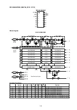
Page 144: ...NJU72340AFH3 DIGITAL_ANALOG IC821 NJU72340A Terminal Functions 144 ...
Page 147: ...2 FL DISPLAY FLD 018BT021GINK FRONT FL101 PIN CONNECTION GRID ASSIGNMENT 147 ...
Page 148: ...ANODE CONNECTION 148 ...
Page 168: ...EXPLODED REF No Part No Part Name Remarks Q ty New Ver S14 nsp SCREW CTW3 6JR VTW3 6JR 2 20 ...

