


Q U I C K R E F E R E N C E G U I D E
LVDT Mode Configuration:
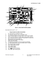
LVDT output signals must be scaled to be compatible with the RD19230
input. These scaling circuit schematics and parameters calculate the needed
component values as defined in the appropriate resolver to digital converter
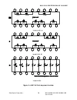
data sheet. The external resistor and capacitor scaling components required
should be mounted on the provided component header’s S1 (See Figure 2,
location 3 & 4) and S2 (See Figure 2, location 15).
To enable LVDT mode:
1) Install TB1- J4 & J5
2) Remove TB1- J6, J7 & J8
3) Remove TB2-J5 & J7
4) Set SW1 and TB2 as indicated in table 7 to obtain the desired resolution.
5) Install user defined 16 pin LVDT component carriers in S1 and S2 as
indicated in Figure 5.
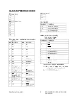
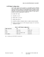
Table 7. LVDT Mode Configuration
LVDT Resolution
D1
D0
8 bits
TB2- J6 IN
SW1-6 “On”
10 bits
SW1-5 “On”
TB2- J8 IN
12 bits
SW1-5 “Off”,TB2- J6 OUT
TB2- J8 IN
14 bits (Note 1)
TB2- J6 IN
TB2- J8 IN
Note 1: Available only on RD-19230EX-300 evaluation card.
Data Device Corporation
RD-19230EX-300 / RD-19240EX-300
User’s
Guide
13
Summary of Contents for RD-19230EX-300
Page 8: ......


