


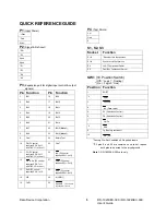


Q U I C K R E F E R E N C E G U I D E
Reference Input Voltage Configuration:
The evaluation board comes preset for a Reference Input Voltage of 26Vrms.
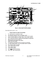
The Reference Input is applied through the RH and RL pins on the P2
connector. (See Figure 2, location 2)
Reference Voltage scaling is accomplished by inserting or removing shorting
jumpers (TB1) on the card as shown in Table 5. (See Figure 2, location 13)
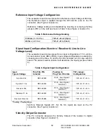
Table 5. Reference Voltage Scaling
115Vrms (10-130Vrms)
TB1-J1, J2 out (Open)
26Vrms (2-40Vrms)
TB1-J1, J2 in (Short)
Signal Input Configuration (Synchro / Resolver & Line to Line
Voltage Level)
The evaluation board comes preset for an input configuration of 11.8 volt line
to line resolver mode (DDC-49530). Input voltage configuration is selected by
choosing one of the three, 16 pin Dip, thin film networks, which come with the
board. The socket insertion location will determine the input type (See Table
6).
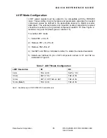
Table 6. Signal Input Configuration
Input
Type & Voltage
Thin Film P/N
to Install
Position to
Plug Thin Film Into
TB1 Jumper
Configuration
Synchro 90v
DDC-49590
location 4)
TB1-J6, J7, J8 in
Synchro 11.8v
DDC-49530
location 4)
TB1-J6, J7, J8 in
Resolver 90v
DDC-49590
location 3)
TB1-J6, J7, J8 in
*Resolver 11.8v
DDC-49530
location 3)
TB1-J6, J7, J8 in
Resolver Direct 2v
DDC-55688
location 3)
TB1-J6, J7, J8 in
*Factory Pre-Settings
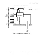
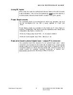
Synchro/ Resolver Signals (S1, S2, S3, S4, Agnd) are input on the P2
connector. (See Figure 2, location 2)
Velocity Output Connector
The P4 connector accesses the Velocity Output of the resolver to digital
converter. (See Figure 2, location 11)
Data Device Corporation
RD-19230EX-300 / RD-19240EX-300
User’s
Guide
12
Summary of Contents for RD-19230EX-300
Page 8: ......


