4: Technical Description
MT1099A-MS
4-7
4.3
Component Locations, Schematics and Parts Lists
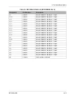
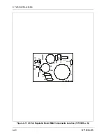
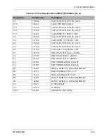
The following pages contain component locations, schematics and parts lists
for the amplifier and regulator boards as well as schematics and parts lists for
the MT-1099A-12 and MT-1099A chassis.
Figure 4-5. DC Out Connector J4 Pinout
Pin
Signal
Description
A
Ground
Chassis ground.
B
RA100 DC PWR
Unswitched power (+12 or 24 Vdc) to
external RF amplifier.
Figure 4-6. DC In Connector J5 Pinout
Pin
Signal
Description
A
GND
Chassis ground.
B
DC IN
Primary input power (+12 or 24 Vdc).
C
N/C
No connection.
D
N/C
No connection.
A
B
A
B
C
D


