PSoC Analog Coprocessor Pioneer Kit Guide, Doc. # 002-11190 Rev. *B
47
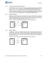
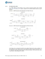
For ‘Current Address Read’ and ‘Sequential Read’, the bus master sends only the slave address.
The memory address used is the same address that was set by the previous ‘Write’ or ‘Selective
Read’ operation. For ‘Selective Read’ operations, after receiving the complete slave address and
memory address, the memory will begin shifting data from the current address on the next clock
Note:
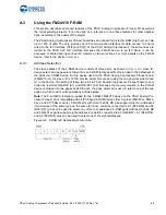
You can communicate with the F-RAM using the Bridge Control Panel (BCP) software similar
to the way you communicate with any other I2C slave device. Refer to the
for
more details on how to use the BCP software to communicate with an I2C slave device. Visit the
CY15FRAMKIT-001 Serial F-RAM Development Kit web page
for code examples and the Arduino
library for details on interfacing I2C F-RAM devices with the PSoC Analog Coprocessor family.
A.4
Migrating Projects Across Different Pioneer Series Kits
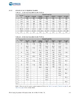
Cypress Pioneer series kits are Arduino Uno-compatible and have some common onboard peripher-
als such as RGB LED, CapSense and User Switch. However, the pin mapping in each of the boards
is different due to differences in pin functions of the PSoC device used. This section lists the pin
mapping of the Pioneer series kits to allow for easy migration of projects across different kits.
In some cases, the pins available on the Pioneer kit headers are a superset of the standard Arduino
Uno pins. For example, J2 contains only one row of pins on the Arduino Uno pin layout while it con-
tains two rows of pins on many of the Pioneer series kits.
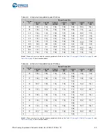
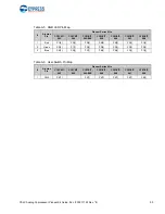
Figure A-9. Pioneer Series Kits Pin Map
Pioneer series kits
J1
J2
J3
J4
1
8
1
2
1
1
8
10
17
18
11
12
CY8 CKIT-040
8
CY8 CKIT- 042 & CY8 CKIT-044
6x 1 header
6x 2 header
9x 2 header
Arduino compatible
I /O headers
Arduino compatible
power header
CY8CKIT-041 8x2
header
CY CKIT-042BLE &CY8CKIT-046
19
20
CY8CKIT-048
10x2 header


