


AN201
Rev 1.5 | 47/91
www.cmostek.com
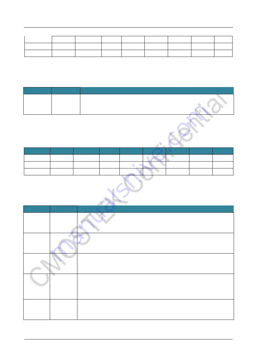
TRISC
TRISC7
TRISC6
TRISC5
TRISC4
TRISC3
TRISC2
TRISC1
TRISC0
Reset
1
1
1
1
1
1
1
1
Type
RW
RW
R
RW
RW
RW
RW
RW
Table 60
. TRISC Bit Function Description
4.1.19 PIE1
(
Addr:0x8C
)
Table 61. PIE1 Register
Name
Bit7
Bit6
Bit5
Bit4
Bit3
Bit2
Bit1
Bit0
PIE1
EEIE
CKMEAIE
-
C2IE
C1IE
OSFIE
TMR2IE
-
Reset
0
0
-
0
0
0
0
-
Type
RW
RW
-
RW
RW
RW
RW
-
Table 62. PIE1 Bit Function Description
Bit
Name
Function
7:0
TRISC<7:0>
PORTC<7:0> port direction control bits
1 = input
0 = output
Bit
Name
Function
7
EEIE
EEPROM write operation completion interrupt enabling bit.
1 = enable write operation completion interrupt
0 = disable write operation completion interrupt
6
CKMEAIE
Fast clock measuring slow clock operation completion interrupt enabling bit.
1 = enable fast clock measuring slow clock operation completion interrupt
0 = disable fast clock measuring slow clock operation completion interrupt
4
C2IE
Comparator 2 interrupt enabling bit
1 = enable the comparator 2 interrupt
0 = disable the comparator 2 interrupt
3
C1IE
Comparator 1 interrupt enabling bit.
1 = enable comparator 1 interrupt
0 = disable comparator 1 interrupt
2
OSFIE
Oscillator failure interrupt enabling bit.
1 = enable the oscillator failure interrupt
0 = disable the oscillator failure interrupt


