CMT2380F17
Rev0.1 | 40/347
www.cmostek.com
SCLK
CSB
SDA
X
X
0
1
2
3
4
5
6
7
0
1
2
3
4
5
6
7
register address
register write data
FCSB
r/w = 0
> 0.5 SCLK cycle
> 0.5 SCLK cycle
Figure 4-6. Transceiver SPI Write Register Timing
4.11.2
Transceiver FIFO Interface Timing
By default, the transceiver provides two independent 32-byte FIFOs for RX and TX. The RX FIFO is used to store received
data in RX mode, and the TX FIFO is to store data to be transmitted in TX mode. Users can set FIFO_MARGE_EN to 1 as well,
thus the two FIFOs are combined into a 64-byte FIFO, available both in TX and RX. By configuring FIFO_RX_TX_SEL, it
indicates whether TX or RX currently is used. In no-combine case, when 32-byte RX FIFO is filled in, to save system operation
time, users can fill in the 32-byte TX FIFO simultaneously for the next transmission.
The FIFO can be accessed via the SPI interface. Users can clear the FIFO by setting the FIFO_CLR_TX/FIFO_CLR_RX bit
and transmit repeated data filled previously by setting FIFO_RESTORE, which avoids data refilling.
When accessing the FIFO, users start from configuring a number of registers involving FIFO read/write mode and some
operating modes settings, as well as some other working modes. Please see AN143-CMT2300A FIFO and Packet Format Usage
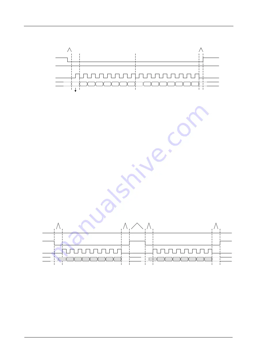
Guide for more details. As shown in below timing diagram for reading and writing, it should be noted that the FCSB control and
CSB control for register access are slightly different. At the beginning of the access, the FCSB pulls down one clock cycle before
sending the rising edge of SCLK. After sending the falling edge of the last SCLK, it pulls up FCSB at least 2us later. The FCSB
must keep pulled up for at least 4us between two consecutive read and write operations. When writing to the FIFO, the first bit of
the data must be ready a half of clock cycle before the first rising edge of SCLK is sent.
SCLK
FCSB
SDA
X
X
FIFO read data
0
1
2
3
4
5
6
7
0
1
2
3
4
5
6
7
X
FIFO read data
CSB
> 1 SCLK cycle
> 4 us
> 2 us
> 2 us
> 1 SCLK cycle
Figure 4-7. SPI Read FIFO Timing
Summary of Contents for CMT2380F17
Page 27: ...CMT2380F17 Rev0 1 27 347 www cmostek com 1 25 Phase Noise...
Page 177: ...CMT2380F17 Rev0 1 177 347 www cmostek com Figure 17 3 PCA Interrupt System...
Page 246: ...CMT2380F17 Rev0 1 246 347 www cmostek com SnMIPS S0MI S1MI 1 P3 3 P4 7...


