


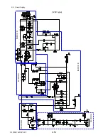
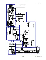


2-5. Power Supply
2-59
CLP-621 & CLP-631
The following circuit reduces the switching noise. So the output noise and the EMI
(electromagnetic interference) noise are suppressed, and the reversal voltage applied to Q1,
DS2 and DS3 is also reduced.
• C13 and R25 connected between drain and source of Q1 / D1, C6, R7 and R5 connected to
the primary winding N1 / C18, C21, R28, FB2 connected to DS3 / C29, C30, R26, FB1
connected to DS2
(2) Driver circuit
The switching FET (Q1) is driven by the control IC (IC1). When power is turned ON, power is
applied to pin 6 (VCC) of IC1 through R3 and R4. Then, the current starts to flow into the
primary winding N2 and voltage is produced there. When the voltage at pin 6 (VCC) reaches
approx. 16V DC, IC1 is activated and a pulse is output from pin 5 (OUT) of IC1 to drive Q1.
When Q1 starts switching, approx. 20-25V DC is supplied from N2 to pin 6 (VCC) of IC1 to
stably activate IC1. During stable oscillation, the switching pulse is continuously output from
pin 5 (OUT) of IC1 to Q1 through R17, R18 and D3. The oscillation frequency is determined by
R12 connected to pin 1 (RT), and the conduction-angle control is made by the control voltage
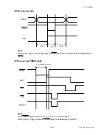
fed from the secondary circuit to pin 2 (FB) of IC1. The following timing chart shows the control
waveforms at various points.
0V
0V
0A
0A
0V
Vds of Q1
Pin 2 of IC1 (FB)
ID of Q1
Secondary current i
flowing into DS2/DS3
Pin 5 of IC1 (OUT)
Vds: Voltage between the drain and source of Q1
Id: Current flowing in the drain of Q1
Summary of Contents for CLP-621
Page 1: ...Technical Manual CLP 621 CLP 631 Thermal Transfer Barcode Label Printer JM74961 00F 1 00E 0701...
Page 2: ...CLP 621 CLP 631 ii Copyright 2007 by CITIZEN SYSTEMS JAPAN CO LTD...
Page 4: ...CHAPTER 1 SPECIFICATIONS CLP 621 CLP 631...
Page 13: ...CHAPTER 2 OPERATING PRINCIPLES CLP 621 CLP 631...
Page 73: ...CHAPTER 3 DISASSEMBLY AND MAINTENANCE CLP 621 CLP 631...
Page 126: ...CLP 621 CLP 631 CHAPTER 4 TROUBLESHOOTING...
Page 138: ...CLP 621 CLP 631 CHAPTER 5 PARTS LISTS...
Page 166: ...Chapter 5 Parts Lists CLP 621 CLP 631 5 29 DRAWING NO 7 Control Panel Unit Rev 0 4 3 2 1 5...
Page 177: ...Chapter 5 Parts Lists CLP 621 CLP 631 5 40 DRAWING NO 10 Accessories Rev 0 3 2 4 1...
Page 179: ...CHAPTER 6 CIRCUIT DIAGRAMS CLP 621 CLP 631...
Page 208: ...APPENDICES CLP 621 CLP 631...
Page 212: ...B Mounting Diagrams AP 5 CLP 621 CLP 631 Main PCB Solder side...
Page 214: ...B Mounting Diagrams AP 7 CLP 621 CLP 631 B 3 Ribbon Main PCB Parts side Solder side...
Page 217: ......


