background image


WM8940 


Rev 4.4 


69


REGISTER BITS BY ADDRESS 

Notes: 

1. Default values of N/A indicate non-latched data bits (e.g. software reset or volume update bits). 

2. Register bits marked as 

“Reserved” should not be changed from the default. 

REGISTER 

ADDRESS 

BIT 

LABEL 

DEFAULT 

DESCRIPTION 

REFER TO 

0 (00h) 

[15:0]  RESET  /  

CHIP_ID 

N/A 

Writing to this register will apply a software reset. 

Reading from this register will return the device id 

Resetting the 
Chip /  

Control Interface 

1 (01h) 

15:9 


00 

Reserved 


VMID_OP_EN 

Enables the non-VMID derived bias current generator 
without enabling the VMID buffer. This bit must be set 
to 1 if output amplifiers are to be enabled before VMID 
is active. Once VMID and VMID buffer are enabled this 
bit can be left set to 0 or left set to 1.  

Power 
Management 

LVLSHIFT_EN 

Enable bit for the level shifters. 1 for normal operation, 
0 for standby. 

Power 
Management 

AUXEN 

Auxiliary input buffer enable 

0 = OFF  

1 = ON 

Auxiliary Inputs 

PLLEN 

PLL enable 

0=PLL off 

1=PLL on 

Master Clock and 
Phase Locked 
Loop (PLL) 

MICBEN 

Microphone Bias Enable 

0 = OFF (high impedance output) 

1 = ON 

Microphone 
Biasing Circuit 

BIASEN 

Analogue amplifier bias control 

0=Disabled 

1=Enabled 

Power 
Management 

2:0 

DEVICE_REVIS
ION 

000 

Readback from this register will return the device 
revision in this position 

Control Interface 

BUFIOEN 

Enable bit for the VMID buffer. The VMID buffer is 
used to maintain a buffered VMID voltage on all 
analogue input and output pins. 1. for normal operation 
0. for standby (where inputs and outputs settle to 
GND). 

Enabling the 
Outputs 

1:0 

VMIDSEL 

00 

Reference string impedance to VMID pin: 

00=off (open circuit) 

01=50k

Ω 

10=250k

Ω 

11=5k

Ω 

Power 
Management 

2 (02h) 

15:5 


000h 

Reserved 


BOOSTEN 

Input BOOST enable 

0 = Boost stage OFF  

1 = Boost stage ON 

Input Boost 


Reserved 


INPPGAEN 

Input microphone PGA enable 

0 = disabled 

1 = enabled 

Input Signal Path 


Reserved 


ADCEN 

ADC Enable Control 

0 = ADC disabled 

1 = ADC enabled 

Analogue to 
Digital Converter 
(ADC) 

3 (03h) 

15:8 


00h 

Reserved 


Summary of Contents for WM8940

Page 1: ...here in the system The WM8940 operates at supply voltages from 2 5 to 3 6V although the digital supplies can operate at voltages down to 1 71V to save power Different sections of the chip can also be powered down under software control using the selectable two or three wire control interface WM8940 is supplied in a very small 4x4mm QFN package offering high levels of functionality in minimum board...

Page 2: ...Filter 4 Notch Filters ALC Limiter DACDAT 50k 50k 4k 5k BYPASS PATH MCLK DCVDD SPKVDD SPKGND BCLK SPKOUTP SPKOUTN L R L R MONOOUT AUX 20k 20k analogue inputs Rbias Mic NOISY GND 12dB to 35 25dB 0 75dB steps MODE GPIO MICN MICP MIC INPUT PGA INPUT BOOST MIXER 0dB 10dB 0dB 10dB PGA Gain Readback GPIO PLL 12dB to 6dB 3dB steps 12dB to 6dB 3dB steps 0dB or 20dB DSP CORE OUTPUTS 57dB to 6dB 1dB steps D...

Page 3: ...ACE TIMING 2 WIRE MODE 18 DEVICE DESCRIPTION 19 INTRODUCTION 19 FEATURES 19 MICROPHONE INPUTS 19 PGA AND ALC OPERATION 19 AUX INPUT 19 ADC 19 HI FI DAC 19 DIGITAL FILTERING 19 OUTPUT MIXING AND VOLUME ADJUST 19 AUDIO INTERFACES 19 CONTROL INTERFACES 20 CLOCKING SCHEMES 20 POWER CONTROL 20 INPUT SIGNAL PATH 20 MICROPHONE INPUTS 20 INPUT PGA VOLUME CONTROL 22 AUXILIARY INPUT 22 INPUT BOOST 23 MICROP...

Page 4: ...ADPHONE OUTPUT 50 MONO OUTPUT 50 DIGITAL AUDIO INTERFACES 51 MASTER AND SLAVE MODE OPERATION 51 AUDIO DATA FORMATS 51 AUDIO INTERFACE CONTROL 53 LOOPBACK 55 AUDIO SAMPLE RATES 55 MASTER CLOCK AND PHASE LOCKED LOOP PLL 55 INTEGER N DIVISION 57 FRACTIONAL K MODE 57 EXAMPLE PLL CONFIGURATION 57 COMPANDING 58 GENERAL PURPOSE INPUT OUTPUT 60 CONTROL INTERFACE 61 SELECTION OF CONTROL MODE AND 2 WIRE MOD...

Page 5: ...TER CHARACTERISTICS 80 TERMINOLOGY 80 DAC FILTER RESPONSES 81 ADC FILTER RESPONSES 81 HIGHPASS FILTER 82 NOTCH FILTERS AND LOW PASS FILTER 82 NOTCH FILTER WORKED EXAMPLE 84 APPLICATIONS INFORMATION 85 RECOMMENDED EXTERNAL COMPONENTS 85 PACKAGE DIAGRAM 86 IMPORTANT NOTICE 87 REVISION HISTORY 88 ...

Page 6: ...N ORDER CODE TEMPERATURE RANGE PACKAGE MOISTURE SENSITIVITY LEVEL PACKAGE BODY TEMPERATURE WM8940CGEFL V 25 C to 85 C 24 lead QFN 4x4x0 9mm Pb free MSL3 260o C WM8940CGEFL RV 25 C to 85 C 24 lead QFN 4x4x0 9mm Pb free tape and reel MSL3 260o C WM8940KGEFL V see Note 25 C to 85 C 24 lead QFN 4x4x0 9mm Pb free MSL3 260o C WM8940KGEFL RV see Note 25 C to 85 C 24 lead QFN 4x4x0 9mm Pb free tape and re...

Page 7: ...ck Input 2 Wire control interface clock input 14 SDIN Digital Input Output 3 Wire control interface data Input 2 Wire control interface data input 15 MODE GPIO Digital Input Control interface mode selection pin or GPIO pin 16 MONOOUT Analogue Output Mono output 17 SPKOUTP Analogue Output Speaker output positive 18 SPKGND Supply Speaker ground 19 SPKOUTN Analogue Output Speaker output negative 20 S...

Page 8: ...torage for 1 year at 30 C 60 Relative Humidity Supplied in moisture barrier bag MSL3 out of bag storage for 168 hours at 30 C 60 Relative Humidity Supplied in moisture barrier bag The Moisture Sensitivity Level for each package type is specified in Ordering Information CONDITION MIN MAX DBVDD DCVDD AVDD SPKVDD supply voltages 0 3V 4 2 Voltage range digital inputs DGND 0 3V DVDD 0 3V Voltage range ...

Page 9: ...37 25 dB Minimum Input PGA Programmable Gain Gain adjusted by INPPGAVOL 14 12 10 dB Programmable Gain Step Size Guaranteed monotonic 0 75 dB Input PGA Mute Attenuation INPPGAMUTE 92 dB Input Gain Boost PGABOOST 0 0 dB Input Gain Boost PGABOOST 1 20 dB Auxiliary Analogue Inputs AUX Full scale Input Signal Level 2 AVDD 3 3 Vrms Input Resistance Input boost and mixer enabled at 0dB gain 20 k Input Ca...

Page 10: ...PKVDD 3 3V 90 85 dBFS Total Harmonic Distortion Noise 5 THD N full scale signal AVDD SPKVDD 3 3V 87 82 dBFS Channel Separation 6 100 dB DAC to Speaker Output SPKOUTP SPKOUTN with 8 bridge tied load Bypass mode Output Power Po Output power is closely correlated with THD see below Total Harmonic Distortion 4 THD Po 350mW RL 8Ω SPKVDD 3 3V 0 03 70 60 dB Signal to Noise Ratio 3 SNR A weighted SPKVDD 3...

Page 11: ...l The reference output signal need not be at full scale amplitude THD is typically measured using an output power of 20mW into a 16ohm load corresponding to a reference signal level of 5dB However the stated test conditions include input signal level signal gain settings output load characteristics and power supply voltages To calculate the ratio the fundamental frequency of the output signal is n...

Page 12: ... R44 0 ALC Limiter AUX2SPK R50 5 BYP2SPK R50 1 DAC2MONO R56 0 AUX2MONO R56 2 BYPL2MONO R56 1 MONOMUTE R56 6 VMID 16Ohm min 8Ohm min BTL Speaker WM8940 Audio Signal Paths Notch Filter MICP MICN DACDAT ADCDAT SPKOUTP AVDD AGND SPEAKER Mixer MICN2INPPGA R44 1 AUX2INPPGA R44 2 Digital Audio Interface MONOATTN R56 7 SPKATTN R54 8 SPKMUTE R54 6 VMID INPPGAMUTE R45 6 K AUX INPPGAVOL R45 5 0 ALCSEL 1 R32 ...

Page 13: ... 8kHz quiescent SLAVE 4 1 0 0 3 11 14 3 Mono Record MIC input 20dB gain 44 1kHz PLL quiescent MASTER 5 3 0 1 9 115 21 0 Mono 16Ω Headphone Playback 0 1mW 1kHz sine wave ac coupled SLAVE 2 8 1 5 1 6 3 7 17 1 Mono 8Ω BTL speaker Playback 44 1kHz 200mW 1kHz sine wave SLAVE 2 8 62 1 6 3 8 216 8 Mono 8Ω BTL speaker Playback 44 1kHz PLL quiescent MASTER 3 9 1 5 1 8 81 21 1 Table 1 Power Consumption Note...

Page 14: ...BVDD AVDD SPKVDD 3 3V DGND AGND SPKGND 0V TA 25o C PARAMETER SYMBOL CONDITIONS MIN TYP MAX UNIT System Clock Timing Information MCLK cycle time TMCLKY MCLK SYSCLK 256fs 81 38 ns MCLK input to PLL Note 1 20 ns MCLK duty cycle TMCLKDS 60 40 40 60 Note 1 PLL pre scaling and PLL N and K values should be set appropriately so that SYSCLK is no greater than 12 288MHz ...

Page 15: ...8V DBVDD AVDD SPKVDD 3 3V DGND AGND SPKGND 0V TA 25o C Slave Mode fs 48kHz MCLK 256fs 24 bit data unless otherwise stated PARAMETER SYMBOL MIN TYP MAX UNIT Audio Data Input Timing Information FRAME propagation delay from BCLK falling edge tDL 10 ns ADCDAT propagation delay from BCLK falling edge tDDA 15 ns DACDAT setup time to BCLK rising edge tDST 10 ns DACDAT hold time from BCLK rising edge tDHT...

Page 16: ...tated PARAMETER SYMBOL MIN TYP MAX UNIT Audio Data Input Timing Information BCLK cycle time tBCY 81 38 ns BCLK pulse width high tBCH 32 55 ns BCLK pulse width low tBCL 32 55 ns FRAME set up time to BCLK rising edge tLRSU 10 ns FRAME hold time from BCLK rising edge tLRH 10 ns DACDAT hold time from BCLK rising edge tDH 10 ns DACDAT set up time to BCLK rising edge tDS 10 ns ADCDAT propagation delay f...

Page 17: ...LK 256fs 24 bit data unless otherwise stated PARAMETER SYMBOL MIN TYP MAX UNIT Program Register Input Information SCLK rising edge to CSB rising edge tSCS 80 ns SCLK pulse cycle time tSCY 200 ns SCLK pulse width low tSCL 80 ns SCLK pulse width high tSCH 80 ns SDIN to SCLK set up time tDSU 40 ns SCLK to SDIN hold time tDHO 40 ns CSB pulse width low tCSL 40 ns CSB pulse width high tCSH 40 ns CSB ris...

Page 18: ...4 bit data unless otherwise stated PARAMETER SYMBOL MIN TYP MAX UNIT Program Register Input Information SCLK Frequency 0 526 kHz SCLK Low Pulse Width t1 1 3 us SCLK High Pulse Width t2 600 ns Hold Time Start Condition t3 600 ns Setup Time Start Condition t4 600 ns Data Setup Time t5 100 ns SDIN SCLK Rise Time t6 300 ns SDIN SCLK Fall Time t7 300 ns Setup Time Stop Condition t8 600 ns Data Hold Tim...

Page 19: ...summed into the input in a flexible fashion either to the input PGA as a second microphone input or as a line input The configuration of this circuit with integrated on chip resistors allows several analogue signals to be summed into the single AUX input if required ADC The mono ADC uses a multi bit high order over sampling architecture to deliver optimum performance with low power consumption Var...

Page 20: ... It operates at low supply voltages and includes the facility to power off any unused parts of the circuitry under software control As a power saving measure ADC or DAC logic in the DSP core is held in its last enabled state when the ADC or DAC is disabled In order to prevent pops and clicks on restart due to residual data in the filters the master clock must remain for at least 64 input samples a...

Page 21: ...ut PGA amplifier negative terminal 1 MICN2INPPGA 1 Connect MICN to input PGA negative terminal 0 MICN not connected to input PGA 1 MICN connected to input PGA amplifier negative terminal 0 MICP2INPPGA 0 Connect input PGA amplifier positive terminal to MICP or VMID 0 input PGA amplifier positive terminal connected to VMID 1 input PGA amplifier positive terminal connected to MICP through variable re...

Page 22: ...nected from the following input BOOST stage 5 0 INPPGAVOL 010000 Input PGA volume 000000 12dB 000001 11 25db 010000 0dB 111111 35 25dB R32 ALC control 1 8 ALCSEL 0 ALC function select 0 ALC off PGA gain set by INPPGAVOL register bits 1 ALC on ALC controls PGA gain Table 4 Input PGA Volume Control AUXILIARY INPUT An auxiliary input circuit Figure 7 is provided which consists of an amplifier which c...

Page 23: ...t using a differential microphone configuration These three inputs can be mixed together and have individual gain boost adjust as shown in Figure 8 To ADC input and output mixers AUX2BOOSTVOL 000 MICP2BOOSTVOL 000 Output from AUX amp Output from input PGA MICP AUX2BOOSTVOL R47 2 0 MICP2BOOSTVOL R47 6 4 INPPGAMUTE R45 6 PGABOOST R47 8 12dB to 6dB 12dB to 6dB 0dB or 20dB Figure 8 Input Boost Stage T...

Page 24: ...hrough boost stage 010 9dB gain through boost stage 111 6dB gain through boost stage Table 7 Input BOOST Stage Control The BOOST stage is enabled under control of the BOOSTEN register bit REGISTER ADDRESS BIT LABEL DEFAULT DESCRIPTION R2 Power management 2 4 BOOSTEN 0 Input BOOST enable 0 Boost stage OFF 1 Boost stage ON Table 8 Input BOOST Enable Control MICROPHONE BIASING CIRCUIT The MICBIAS out...

Page 25: ...portional to AVDD With a 3 3V supply voltage the full scale level is 1 0Vrms Any voltage greater than full scale may overload the ADC and cause distortion ADC DIGITAL FILTERS The ADC filters perform true 24 bit signal processing to convert the raw multi bit over sampled data from the ADC to the correct sampling frequency to be output on the digital audio interface The digital filter path is illust...

Page 26: ...hen HPFAPP 1 are shown in Table 14 REGISTER ADDRESS BIT LABEL DEFAULT DESCRIPTION R14 ADC Control 8 HPFEN 1 High Pass Filter Enable 0 disabled 1 enabled 7 HPFAPP 0 Select audio mode or application mode 0 Audio mode 1st order fc 3 7Hz 1 Application mode 2nd order fc HPFCUT 6 4 HPFCUT 000 Application mode cut off frequency See Table 14 for details Table 13 ADC Filter Select HPFCUT FS KHZ SR 101 100 ...

Page 27: ...er coefficients must be entered using a sign magnitude notation REGISTER ADDRESS BIT LABEL DEFAULT DESCRIPTION R16 Notch Filter 0A 15 NF0_UP 0 Notch filter 0 update The notch filter 0 values used internally only update when one of the NF0_UP bits is set high 14 NF0_EN 0 Notch filter 0 enable 0 Disabled 1 Enabled 13 0 NF0_A0 0 Notch filter 0 a0 coefficient R17 Notch Filter 0B 15 NF0_UP 0 Notch filt...

Page 28: ...ly only update when one of the NFU bits is set high 14 NF3_EN 0 Notch filter 3 enable 0 Disabled 1 Enabled 13 0 NF3_A0 0 Notch filter 3 a0 coefficient R23 Notch Filter 3B 15 NF3_UP 0 Notch filter 3 update The notch filter 3 values used internally only update when one of the NFU bits is set high 14 NF3_LP 0 Notch filter 3 mode select 0 Notch Filter mode 1 Low Pass Filter mode 13 0 NF3_A1 0 Notch fi...

Page 29: ... for x 0 REGISTER ADDRESS BIT LABEL DEFAULT DESCRIPTION R15 ADC Digital Volume 7 0 ADCVOL 7 0 11111111 0dB ADC Digital Volume Control 0000 0000 Digital Mute 0000 0001 127dB 0000 0010 126 5dB 0 5dB steps up to 1111 1111 0dB Table 19 ADC Volume INPUT LIMITER AUTOMATIC LEVEL CONTROL ALC The WM8940 has an automatic PGA gain control circuit which can function as an input peak limiter or as an automatic...

Page 30: ...29 25dB 101 23 25dB 100 17 25dB 011 11 25dB 010 5 25dB 001 0 75dB 000 6 75dB 8 ALCSEL 0 ALC function select see Note 0 ALC disabled 1 ALC Enabled R33 21h ALC Control 2 3 0 ALCLVL 3 0 1011 6dB ALC target sets signal level at ADC input 1111 1 5dBFS 1110 1 5dBFS 1101 3dBFS 1100 4 5dBFS 1011 6dBFS 1010 7 5dBFS 1001 9dBFS 1000 10 5dBFS 0111 12dBFS 0110 13 5dBFS 0101 15dBFS 0100 16 5dBFS 0011 18dBFS 001...

Page 31: ...ain ramp down time ALCMODE 0 Per step Per 6dB 90 of range 0000 104us 832us 6ms 0001 208us 1 66ms 12ms 0010 416us 3 33ms 24ms time doubles with every step 1010 or higher 106ms 852ms 6 13s 0010 726us 6dB ALC attack gain ramp down time ALCMODE 1 Per step Per 6dB 90 of range 0000 22 7us 182 4us 1 31ms 0001 45 4us 363us 2 62ms 0010 90 8us 726us 5 23ms time doubles with every step 1010 or higher 23 2ms ...

Page 32: ...eration LIMITER MODE In limiter mode the ALC will reduce peaks that go above the threshold level but will not increase the PGA gain beyond the starting level The starting level is the PGA gain setting when the ALC is enabled in limiter mode If the ALC is started in limiter mode this is the gain setting of the PGA at start up If the ALC is switched into limiter mode after running in ALC mode the st...

Page 33: ...re faster than in ALC mode The time constants are shown below in terms of a single gain step a change of 6dB and a change of 90 of the PGAs gain range Note that these times will vary slightly depending on the sample rate used specified by the SR register NORMAL MODE ALCMODE 0 Normal Mode ALCATK tATK tATK6dB tATK90 0000 104µs 832µs 6ms 0001 208µs 1 66ms 12ms 0010 416µs 3 33ms 24ms 0011 832µs 6 66ms...

Page 34: ... 22 7µs 182µs 1 31ms 0001 45 4µS 363µs 2 62ms 0010 90 8µS 726µs 5 23ms 0011 182µS 1 45ms 10 5ms 0100 363µS 2 91ms 20 9ms 0101 726µS 5 81ms 41 8ms 0110 1 45ms 11 6ms 83 7ms 0111 2 9ms 23 2ms 167ms 1000 5 81ms 46 5ms 335ms 1001 11 6ms 93ms 669ms 1010 23 2ms 186ms 1 34s Attack Time s ALCMODE 1 Limiter Mode ALCDCY tDCYLIM tDCYLIM6dB tDCYLIM90 0000 90 8µs 726µs 5 23ms 0001 182µS 1 45ms 10 5ms 0010 363µ...

Page 35: ... In normal mode ALCMAX sets the maximum boost which can be applied to the signal In limiter mode ALCMAX will normally have no effect assuming the starting gain value is less than the maximum gain specified by ALCMAX because the maximum gain is set at the starting gain level ALCMIN sets the minimum gain value which can be applied to the signal PGA Gain 000000 12dB PGA Gain 111111 35 25dB ALCMAX ALC...

Page 36: ...d ALCMIN limits ALC HOLD TIME NORMAL MODE ONLY In Normal mode the ALC has an adjustable hold time which sets a time delay before the ALC begins its decay phase gain increasing The hold time is set by the ALCHLD register REGISTER ADDRESS BIT LABEL DEFAULT DESCRIPTION R33 ALC Control 2 7 4 ALCHLD 0000 ALC hold time before gain is increased Table 26 ALC Hold Time If the hold time is exceeded this ind...

Page 37: ...WM8940 Rev 4 4 37 Input Signal Output of PGA ALCLVL PGA Gain Figure 15 ALCLVL ...

Page 38: ... large signal occurs just after a period of quiet the ALC circuit includes a limiter function If the ADC input signal exceeds 87 5 of full scale 1 16dB the PGA gain is ramped down at the maximum attack rate as when ALCATK 0000 until the signal level falls below 87 5 of full scale This function is automatically enabled whenever the ALC is enabled Note If ALCATK 0000 then the limiter makes no differ...

Page 39: ...e signal is quiet The table below summarises the noise gate control register The NGTH control bits set the noise gate threshold with respect to the ADC full scale range The threshold is adjusted in 6dB steps Levels at the extremes of the range may cause inappropriate operation so care should be taken with set up of the function The noise gate only operates in conjunction with the ALC and cannot be...

Page 40: ...WM8940 40 Rev 4 4 Input Signal Output of PGA ALCLVL PGA Gain Figure 17 ALC Operation Above Noise Gate Threshold Input Signal Output of PGA ALCLVL PGA Gain NGTH Figure 18 Noise Gate Operation ...

Page 41: ...L AUDIO INTERFACE DIGITAL GAIN DIGITAL FILTERS INTERP SDM DAC DIGITAL PEAK LIMITER DAC DIGITAL FILTERS Figure 19 DAC Digital Filter Path The analogue output from the DAC can then be mixed with the AUX analogue input and the ADC analogue input The mix is fed to the output drivers SPKOUTP N and MONOOUT MONOOUT can drive a 16 or 32 headphone or line output or can be a buffered version of VMID When MO...

Page 42: ...p true 24 bit digital interpolation filters The bit stream data enters a multi bit sigma delta DAC which converts it to a high quality analogue audio signal The multi bit DAC architecture reduces high frequency noise and sensitivity to clock jitter The DAC output defaults to non inverted Setting DACPOL will invert the DAC output phase AUTOMUTE The DAC has an automute function which applies an anal...

Page 43: ...lls below the lower threshold the signal is amplified at a specific decay rate controlled by LIMDCY register bits until a gain of 0dB is reached Both threshold levels are controlled by the LIMLVL register bits The upper threshold is 0 5dB above the value programmed by LIMLVL and the lower threshold is 0 5dB below the LIMLVL value VOLUME BOOST The limiter has programmable upper gain which boosts si...

Page 44: ...s 0101 24ms 0110 48ms 0111 96ms 1000 192ms 1001 384ms 1010 768ms 1011 to 1111 1 536s 3 0 LIMATK 0010 Limiter Attack time per 6dB gain change for 44 1kHz sampling Note that these will scale with sample rate 0000 94us 0001 188s 0010 375us 0011 750us 0100 1 5ms 0101 3ms 0110 6ms 0111 12ms 1000 24ms 1001 48ms 1010 96ms 1011 to 1111 192ms R25 DAC digital limiter control 2 6 4 LIMLVL 000 Programmable si...

Page 45: ...UTN OUTPUTS The SPKOUT pins can drive a single bridge tied 8Ω speaker or two headphone loads of 16 or 32 or a line output see Headphone Output and Line Output sections respectively The signal to be output on SKPKOUT comes from the Speaker Mixer circuit and can be any combination of the DAC output the Bypass path output of the boost stage and the AUX input The SPKOUTP N volume is controlled by the ...

Page 46: ...enable 1 Change gain on zero cross only 0 Change gain immediately 6 SPKMUTE 1 Speaker output mute enable 0 Speaker output enabled 1 Speaker output muted VMIDOP 5 0 SPKVOL 5 0 111001 0dB Speaker Volume Adjust 111111 6dB 111110 5dB 1 0 dB steps 111001 0dB 000000 57dB Table 35 SPKOUT Volume Control ZERO CROSS TIMEOUT A zero cross timeout function is also provided so that if zero cross is enabled on t...

Page 47: ...t boost stage to mono mixer input 0 non selected 1 selected 0 DAC2MONO 0 Output of DAC to mono mixer input 0 not selected 1 selected Table 37 Mono Mixer Control ENABLING THE OUTPUTS Each analogue output of the WM8940 can be separately enabled or disabled The analogue mixer associated with each output has a separate enable All outputs are disabled by default To save power unused parts of the WM8940...

Page 48: ...ULT DESCRIPTION R49 0 VROI 0 VREF AVDD 2 to analogue output resistance 0 approx 1k 1 approx 30 k Table 39 Disabled Outputs to VREF Resistance A dedicated buffer is available for tying off unused analogue I O pins as shown in Figure 21 This buffer can be enabled using the BUFIOEN register bit Table 40 summarises the tie off options for the speaker and mono output pins AVDD 2 AVDD 2 Used to tie off ...

Page 49: ... clocked from a slow clock with period 221 x MCLK enabled using the SLOWCLKEN register bit GPIOPOL CSB GPIO SPKNEN SPKPEN MONOEN SPEAKER ENABLED MONO OUTPUT ENABLED 0 0 0 X No No 0 0 1 X Yes No 0 1 X 0 No No 0 1 X 1 No Yes 1 0 X 0 No No 1 0 X 1 No Yes 1 1 0 X No No 1 1 1 X Yes No Table 41 Output Switch Operation GPIOSEL 001 THERMAL SHUTDOWN The speaker outputs can drive very large currents To prot...

Page 50: ...to the DC offset on the SPROUTP and SPKOUTN pins therefore no DC blocking capacitors are required This saves space and material cost in portable applications It is recommended to connect the DC coupled outputs only to headphones and not to the line input of another device Although the built in short circuit protection will prevent any damage to the headphone outputs such a connection may be noisy ...

Page 51: ...and thus controls sequencing of the data transfer on ADCDAT and DACDAT To set the device to master mode register bit MS should be set high In slave mode MS 0 the WM8940 responds with data to clocks it receives over the digital audio interfaces AUDIO DATA FORMATS In Left Justified mode the MSB is available on the first rising edge of BCLK following an FRAME transition The other bits up to the LSB a...

Page 52: ...IGHT PHASE FRAME BCLK DACDAT ADCDAT 1 fs n 3 2 1 n 2 n 1 LSB MSB 1 BCLK Figure 27 I2 S Audio Interface assuming n bit word length In DSP PCM mode the left channel MSB is available on either the 1st Mode B the 2nd Mode A rising edge of BCLK selectable by FRAMEP following a rising edge of FRAME Right channel data immediately follows left channel data Depending on word length BCLK frequency and sampl...

Page 53: ...k This may result in short BCLK pulses at the end of a frame if there is a non integer ratio of BCLKs to FRAME clocks REGISTER ADDRESS BIT LABEL DEFAULT DESCRIPTION R4 Audio interface control 9 LOUTR 0 LOUTR control 0 normal 1 Input mono channel data output on both left and right channels 8 BCP 0 BCLK polarity 0 normal 1 inverted 7 FRAMEP 0 Frame clock polarity for RJ LJ and I2 S formats 0 normal ...

Page 54: ...cted the device will operate in 24 bit mode REGISTER ADDRESS BIT LABEL DEFAULT DESCRIPTION R6 Clock generation control 8 CLKSEL 1 Controls the source of the clock for all internal operation 0 MCLK 1 PLL output 7 5 MCLKDIV 010 Sets the scaling for either the MCLK or PLL clock output under control of CLKSEL 000 divide by 1 001 divide by 1 5 010 divide by 2 011 divide by 3 100 divide by 4 101 divide ...

Page 55: ...REGISTER ADDRESS BIT LABEL DEFAULT DESCRIPTION R7 Additional control 3 1 SR 000 Approximate sample rate configures the coefficients for the internal digital filters 000 48kHz 001 32kHz 010 24kHz 011 16kHz 100 12kHz 101 8kHz 110 111 reserved Table 45 Sample Rate Control MASTER CLOCK AND PHASE LOCKED LOOP PLL The WM8940 has an on chip phase locked loop PLL circuit that can be used to Generate master...

Page 56: ...V 3 0 see figure 34 The divided clock SYSCLK can be used to clock the WM8940 DSP REGISTER ADDRESS BIT LABEL DEFAULT DESCRIPTION R36 PLL N value 7 PLL_POWERDOWN 0 PLL POWER 0 ON 1 OFF 6 FRACEN 1 Fractional Divide within the PLL 0 Disabled Lower Power 1 Enabled 5 4 PLLPRESCALE 00 00 MCLK input multiplied by 2 01 MCLK input not divided 10 Divide MCLK by 2 before input to PLL 11 Divide MCLK by 4 befor...

Page 57: ...be set The relationship between the required division R the fractional division K 23 0 and the integer division N 3 0 is K 224 R N where 0 R N 1 and K is rounded to the nearest whole number EXAMPLE PLL CONFIGURATION PLL input clock f1 is 12MHz and the required clock SYSCLK is 12 288MHz R should be chosen to ensure 5 N 13 There is a fixed divide by 4 in the PLL and a selectable divider MCLKDIV 3 0 ...

Page 58: ... 7 482296 Table 49 PLL Frequency Examples COMPANDING The WM8940 supports A law and law companding on both transmit ADC and receive DAC sides Companding can be enabled on the DAC or ADC audio interfaces by writing the appropriate value to the DAC_COMP or ADC_COMP register bits respectively If packed mode companding is desired the WL8 register bit is available It will override the normal audio inter...

Page 59: ...nverts 13 bits law or 12 bits A law to 8 bits using non linear quantization The input data range is separated into 8 levels allowing low amplitude signals better precision than that of high amplitude signals This is to exploit the operation of the human auditory system where louder sounds do not require as much resolution as quieter sounds The companded signal is an 8 bit word containing sign 1 bi...

Page 60: ...from the GPIO control register R8 The GPIOSEL bits allow the chosen pin to be configured to perform a variety of useful tasks as shown in Table 57 Note that SLOWCLKEN must be enabled when using the jack detect function REGISTER ADDRESS BIT LABEL DEFAULT DESCRIPTION R8 GPIO control 5 4 OPCLKDIV 00 PLL Output clock division ratio 00 divide by 1 01 divide by 2 10 divide by 3 11 divide by 4 3 GPIOPOL ...

Page 61: ...undriven or driven high at start up Specifically MODE must be high or hi Z during an initial write to the control interface which sets the MODE_GPIO register bit After MODE_GPIO has been set 3 wire mode selection is overridden internally and the MODE pin can be used freely as a GPIO input or output MODE PAD WM8940 CLOCK_IN Partner Device DIGITAL CORE DFF D ENB Vdd GPIO_OE GPIO_OUT MODE Pull up hol...

Page 62: ...ESS BIT LABEL DEFAULT DESCRIPTION R9 Control Interface 1 AUTOINC 1 Auto Incremental write enable 0 Auto Incremental writes disabled 1 Auto Incremental writes enabled Table 55 Control Interface 3 WIRE SERIAL CONTROL MODE In 3 wire mode every rising edge of SCLK clocks in one data bit from the SDIN pin A rising edge on CSB GPIO latches in a complete control word consisting of the last 16 bits B23 B2...

Page 63: ...WM8940 returns to the idle condition and wait for a new start condition and valid address During a write once the WM8940 has acknowledged a correct address the controller sends the first byte of control data B23 to B16 i e the WM8940 8 bit register address The WM8940 then acknowledges the first data byte by pulling SDIN low for one clock pulse The controller then sends the second byte of control d...

Page 64: ...pply voltage for all four supplies However digital and analogue supplies should be routed and decoupled separately on the PCB to keep digital switching noise out of the analogue signal paths RECOMMENDED POWER UP DOWN SEQUENCE In order to minimise output pop and click noise it is recommended that the WM8940 WM8941 device is powered up and down using one of the following sequences Power Up 1 Turn on...

Page 65: ...tware reset 10 Turn off external power supply voltages Notes 1 This step enables the internal device bias buffer and the VMID buffer for unassigned inputs outputs This will provide a startup reference for all inputs and outputs This will cause the inputs and outputs to ramp towards VMID in a way that is controlled and predictable 2 Choose the value of VMIDSEL bits based on the startup time VMIDSEL...

Page 66: ...t 1 3 BIASEN 0 Analogue amplifier bias control 0 Disabled 1 Enabled Table 58 BIASEN Control ESTIMATED SUPPLY CURRENTS When either the DAC or ADC are enabled it is estimated that approximately 4mA will be drawn from DCVDD when fs 48kHz This will be lower at lower sample rates When the PLL is enabled an additional 700 microamps will be drawn from DCVDD Table 59 shows the estimated 3 3V AVDD current ...

Page 67: ... VMID decoupling cap to follow a soft start profile which minimises pops This soft start profile has minimal impact on VMID charge time Fast VMID discharge is enabled using TOGGLE Setting to 1 opens a low impedance discharge path from VMID to GND This function can be used during power down to reduce the discharge time of the VMID decoupling cap Must be set to 0 for normal operation REGISTER ADDRES...

Page 68: ... 21 ALC control 2 0 0 0 0 0 0 0 0 0000_0000_0000_1011 34 22 ALC control 3 0 0 0 0 0 0 0 ALCMODE 0000_0000_0011_0010 35 23 Noise Gate 0 0 0 0 0 0 0 0 0 0 0 0 NGEN 0000_0000_0000_0000 36 24 PLL N 0 0 0 0 0 0 0 0 PLL_POWERDO WN FRACEN 0000_0000_0100_1000 37 25 PLL K 1 0 0 0 0 0 0 0 0 0 0 0000_0000_0000_1100 38 26 PLL K 2 0 0 0 0 0 0 0 0000_0000_1001_0011 39 27 PLL K 3 0 0 0 0 0 0 0 0000_0000_1110_100...

Page 69: ...uffer enable 0 OFF 1 ON Auxiliary Inputs 5 PLLEN 0 PLL enable 0 PLL off 1 PLL on Master Clock and Phase Locked Loop PLL 4 MICBEN 0 Microphone Bias Enable 0 OFF high impedance output 1 ON Microphone Biasing Circuit 3 BIASEN 0 Analogue amplifier bias control 0 Disabled 1 Enabled Power Management 2 0 DEVICE_REVIS ION 000 Readback from this register will return the device revision in this position Con...

Page 70: ... 7 FRAMEP 0 Frame clock polarity 0 normal 1 inverted Digital Audio Interfaces DSP Mode control 1 Configures the interface so that MSB is available on 1st BCLK rising edge after FRAME rising edge 0 Configures the interface so that MSB is available on 2nd BCLK rising edge after FRAME rising edge 6 5 WL 10 Word length 00 16 bits 01 20 bits 10 24 bits 11 32 bits Digital Audio Interfaces 4 3 FMT 10 Aud...

Page 71: ... Audio Interfaces 6 06h 15 9 00h Reserved 8 CLKSEL 1 Controls the source of the clock for all internal operation 0 MCLK 1 PLL output Digital Audio Interfaces 7 5 MCLKDIV 010 Sets the scaling for either the MCLK or PLL clock output under control of CLKSEL 000 divide by 1 001 divide by 1 5 010 divide by 2 011 divide by 3 100 divide by 4 101 divide by 6 110 divide by 8 111 divide by 12 Digital Audio ...

Page 72: ... as a GPIO pin 0 MODE is an input MODE selects 2 wire mode when low and 3 wire mode when high 1 MODE can be an input or output under the control of the GPIO control register Interface operates in 3 wire mode regardless of what happens on the MODE pin Control Interface 6 0 Reserved 5 4 OPCLKDIV 00 PLL Output clock division ratio 00 divide by 1 01 divide by 2 10 divide by 3 11 divide by 4 General Pu...

Page 73: ...lication mode 2nd order fc HPFCUT Analogue to Digital Converter ADC 6 4 HPFCUT 000 Application mode cut off frequency See Table 14 for details Analogue to Digital Converter ADC 3 1 00 Reserved 0 ADCPOL 0 ADC Polarity 0 normal 1 inverted Analogue to Digital Converter ADC 15 0Fh 15 8 00h Reserved 7 0 ADCVOL 11111111 ADC Digital Volume Control 0000 0000 Digital Mute 0000 0001 127dB 0000 0010 126 5dB ...
Page 74: ...logue to Digital Converter ADC 13 0 NF2_A0 0000h Notch Filter 2 a0 coefficient Analogue to Digital Converter ADC 21 15h 15 NF2_UP 0 Notch filter 2 update The notch filter 2 values used internally only update when one of the NFU bits is set high Analogue to Digital Converter ADC 14 0 Reserved 13 0 NF2_A1 0000h Notch Filter 2 a1 coefficient Analogue to Digital Converter ADC 22 16h 15 NF3_UP 0 Notch ...

Page 75: ...us 0001 188s 0010 375us 0011 750us 0100 1 5ms 0101 3ms 0110 6ms 0111 12ms 1000 24ms 1001 48ms 1010 96ms 1011 to 1111 192ms Output Signal Path 25 19h 15 7 000h Reserved 6 4 LIMLVL 000 DAC Limiter Programmable signal threshold level determines level at which the limiter starts to operate 000 1dB 001 2dB 010 3dB 011 4dB 100 5dB 101 to 111 6dB Output Signal Path 3 0 LIMBOOST 0000 DAC Limiter volume bo...

Page 76: ...ation 0 Normal mode 1 Limiter mode Input Limiter Automatic Level Control ALC 7 4 ALCDCY 0011 Decay gain ramp up time Input Limiter Automatic Level Control ALC 3 0 ALCATK 0010 ALC attack gain ramp down time Input Limiter Automatic Level Control ALC 35 23h 15 4 000h Reserved 3 NGEN 0 Noise gate function enable 1 enable 0 disable Input Limiter Automatic Level Control ALC 2 0 NGTH 000 Noise gate thres...

Page 77: ... AVDD Input Signal Path 7 4 0h Reserved 3 AUXMODE 0 Auxiliary Input Mode 0 inverting buffer 1 mixer on chip input resistor bypassed Input Signal Path 2 AUX2INPPGA 0 Select AUX amplifier output as input PGA signal source 0 AUX not connected to input PGA 1 AUX connected to input PGA amplifier negative terminal Input Signal Path 1 MICN2INPPGA 1 Connect MICN to input PGA negative terminal 0 MICN not c...

Page 78: ...e auxiliary amplifier to the input boost stage 000 Path disabled disconnected 001 12dB gain through boost stage 010 9dB gain through boost stage 111 6dB gain through boost stage Input Signal Path 48 30h 15 0 0000h Reserved 49 31h 15 2 0000h Reserved 1 TSDEN 1 Thermal Shutdown Enable 0 thermal shutdown disabled 1 thermal shutdown enabled Output Switch 0 VROI 0 VREF AVDD 2 or 1 5xAVDD 2 to analogue ...

Page 79: ... dB steps 111001 0dB 000000 57dB Analogue Outputs 55 37h 15 0 0000h Reserved 56 38h 15 8 00h Reserved 7 MONOATTN 0 Attenuation control for bypass path output of input boost stage to mono mixer input 0 0dB 1 10dB Analogue Outputs 6 MONOMUTE 0 MONOOUT Mute Control 0 No mute 1 Output muted During mute the mono output will output VMID which can be used as a DC reference for a headphone out Analogue Ou...
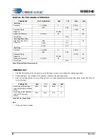
Page 80: ... Delay 29 fs Table 61 Digital Filter Characteristics TERMINOLOGY 1 Stop Band Attenuation dB the degree to which the frequency spectrum is attenuated outside audio band 2 Pass band Ripple any variation of the frequency response in the pass band region 3 Note that this delay applies only to the filters and does not include additional delays through other digital circuits See Table 62 for the total d...

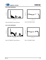
Page 81: ... Frequency Fs Response dB Figure 38 DAC Digital Filter Frequency Response Figure 39 DAC Digital Filter Ripple ADC FILTER RESPONSES 120 100 80 60 40 20 0 0 0 5 1 1 5 2 2 5 3 Frequency Fs Response dB 0 2 0 15 0 1 0 05 0 0 05 0 1 0 15 0 2 0 0 1 0 2 0 3 0 4 0 5 Frequency Fs Response dB Figure 40 ADC Digital Filter Frequency Response Figure 41 ADC Digital Filter Ripple ...

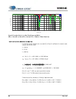
Page 82: ...800 1000 1200 Frequency Hz Response dB Figure 44 ADC High pass Filter Responses 24kHz HPFAPP 1 all cut off settings shown Figure 45 ADC Highpass Filter Responses 12kHz HPFAPP 1 all cutoff settings shown NOTCH FILTERS AND LOW PASS FILTER The WM8940 supports four programmable notch filters The fourth notch filter can be configured as a low pass filter The following illustrates three digital notch fi...

Page 83: ...200 500 1k 2k 5k 10k Frequency Hz Figure 46 ADC Notch Filter Responses 48kHz fc 100Hz 1kHz 10kHz fb 100Hz 600Hz 2kHz 60 0 55 50 45 40 35 30 25 20 15 10 5 R E S P O N S E dB 20 20k 50 100 200 500 1k 2k 5k 10k Frequency Hz T T Figure 47 ADC Low Pass Filter Responses 48kHz fc 1kHz 5kHz 10kHz ...

Page 84: ...andwidth fc 1000 Hz fb 100 Hz fs 48000 Hz s c 0 f f 2 w 2 x 1000 48000 0 1308996939 rads s b b f f 2 w 2 x 100 48000 0 01308996939 rads 2 w tan 1 2 w tan 1 a b b 0 2 9 0130899693 0 tan 1 2 9 0130899693 0 tan 1 0 9869949627 w cos a 1 a 0 0 1 1308996939 0 cos 9869949627 0 1 1 969995945 NFn_A0 a0 x 213 8085 rounded to nearest whole number NFn_A1 a1 x 212 8069 rounded to nearest whole number These val...

Page 85: ...WM8940 Rev 4 4 85 APPLICATIONS INFORMATION RECOMMENDED EXTERNAL COMPONENTS Figure 49 Recommended External Components ...

Page 86: ...FOR FURTHER INFORMATION REGARDING PCB FOOTPRINTS AND QFN PACKAGE SOLDERING 7 THIS DRAWING IS SUBJECT TO CHANGE WITHOUT NOTICE A3 G T H W b Exposed lead Half etch tie bar Dimensions mm Symbols MIN NOM MAX NOTE A A1 A3 0 80 0 85 0 90 0 05 0 035 0 0 203 REF b D D2 E E2 e L 0 30 0 20 4 00 BSC 2 60 2 50 2 40 0 50 BSC 0 35 0 40 0 45 2 2 4 00 BSC 2 60 2 50 2 40 0 10 aaa bbb ccc REF 0 10 0 10 JEDEC MO 220...

Page 87: ... DEATH PERSONAL INJURY OR SEVERE PROPERTY OR ENVIRONMENTAL DAMAGE CRITICAL APPLICATIONS CIRRUS LOGIC PRODUCTS ARE NOT DESIGNED AUTHORIZED OR WARRANTED FOR USE IN PRODUCTS SURGICALLY IMPLANTED INTO THE BODY AUTOMOTIVE SAFETY OR SECURITY DEVICES NUCLEAR SYSTEMS LIFE SUPPORT PRODUCTS OR OTHER CRITICAL APPLICATIONS INCLUSION OF CIRRUS LOGIC PRODUCTS IN SUCH APPLICATIONS IS UNDERSTOOD TO BE FULLY AT TH...

Page 88: ...ed to correct MONOOUT and SPKOUT paths 26 09 11 4 3 JMacD Order codes changed from WM8940GEFL V and WM8940GEFL RV to WM8940CGEFL V and WM8940CGEFL RV to reflect change to copper wire bonding 26 09 11 4 3 JMacD Package Drawing changed to DM102 C 09 12 21 4 4 PH New order codes added to reflect PCN 2020 141 ...

Reviews: