DS726PP2
73
CS4525
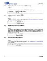
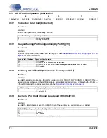
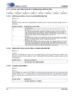
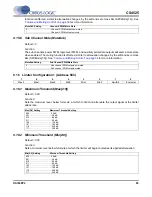
9.3.5
Aux Serial Port Left Channel Data Select (LChDSel[1:0])
Default = 00
Function:
Selects the data to be sent over the left channel of the auxiliary port serial data output signal.
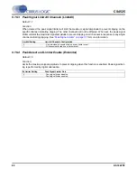
9.4
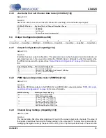
Output Configuration (Address 04h)
9.4.1
Output Configuration (OutputCfg[1:0])
Default = 00
Function:
Identifies the power output configuration. This parameter can only be changed when all modulators and
associated logic are in the power-down state (the PDnAll bit is set). Attempts to write this register while
the PDnAll is cleared will be ignored. See
“Output Channel Configurations” on page 45
for more informa-
tion.
9.4.2
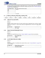
PWM Signals Output Data Select (PWMDSel[1:0])
Default = 00
Function:
Selects the PWM data output on the PWM_SIG1 and PWM_SIG2 output signals.See
Level Output Configurations” on page 49
for more information.
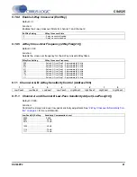
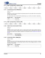
9.4.3
Channel Delay Settings (OutputDly[3:0])
Default = 0000
Function:
The channel delay bits allow delay adjustment of each of the power output audio channels. The value of
this register determines the amount of delay inserted in the output path. The delay time is calculated by
multiplying the register value by the period of the SYS_CLK or crystal input clock source. These bits can
LChDSel[1:0] Setting
Aux Serial Port Left Channel Output Data Source
00 ........................................ Channel A.
01 ........................................ Channel B.
10 ........................................ Sub Channel.
11......................................... Channel B crossover low-pass output.
7
6
5
4
3
2
1
0
OutputCfg1
OutputCfg0
PWMDSel1
PWMDSel0
OutputDly3
OutputDly2
OutputDly1
OutputDly0
OutputCfg[1:0] Setting
Power Output Configuration
00 ........................................ Channel 1 & 2 Full-Bridge.
01 ........................................ Channel 1 & 2 Half- Sub Channel Full-Bridge.
10 ........................................ Channel 1 Parallel Full-Bridge.
11......................................... Reserved.
PWMDSel Setting
PWM Signal Output Mapping
00 ........................................ PWM_SIG1 output disabled.
PWM_SIG2 output disabled.
01 ........................................ Channel 1 output on PWM_SIG1.
Channel 2 output on PWM_SIG2.
10 ........................................ Channel 1 output on PWM_SIG1.
Sub Channel output on PWM_SIG2.
11......................................... Channel 2 output on PWM_SIG1.
Sub Channel output on PWM_SIG2.

