background image

Broadcom

®


August 27, 2015 • 920737TAG04-HWUM101-RDS

Page 16

Schematics


BCM920737TAG-04 WICED Smart Tag Hardware User Manual

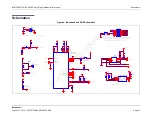
Figure 5:  RF Schematics

Note: 
Antenna matching network.
Please note that the
value on those components
may vary by different
layout and different
housing design.

Note:
"Pi" harmonic
filter for
2nd and 3rd
harmonic

+/- 0.1pF

+/- 0.1pF

Glass XTAL 3.2x2.5

Layout note: use antenna from 200-121921-0000 P1

VDDC and VDDRF can come from internal LDO or external LDO
internal LDO: RD6=BC, RD5=BC
external LDO: RD6=AC, RD5=AC

GND

FEED

1P2VC

VDDIO

1P2VRF

LDOext

LDOint

LDOint

LDOext

EXT_LDO_IN

EXT_LDO_IN

P12/P26

2,5

P11/P27

2,5

R25

0

R26
0 (DNI)

C9

1uF

C15
1.8pF

C21
12pF

RD6

0

INSTALL POSITION B

A

B

C

U2B
BCM20737A1KML2G

QFN32H_0.5mm

VD

D

F

E

5

V

DDV

CO

7

RF

6

XTALI

9

XTALO

10

L

D

OOU

T

3

LD

O

IN

2

VD

D

IF

4

VD

D

PL

L

8

FB2

120Ohms

J1
20279-001E-04

RF

_

IN

S

GN

D

G1

GN

D

G2

Y1
24.000MHz

1

3

2

4

C6
47uF

RD5

0

INSTALL POSITION B

A

B

C

C20
12pF

L1 10uH

1

2

C8

2.2uF

C13

0.01uF

C12

0.01uF

C17

1.8pF (DNI)

FB1
120Ohms

RD7
0

INSTALL POSITION A

A

B

C

R24

2.7nH

C31
22uF

XC9265B1214R-G

U4

DFN6H_0.55mm

VIN

6

LX

1

VOUT

3

NC

5

CE

4

HS-GND

H

GND

2

C14
1.8pF

C11

10pF

C16

1.8pF (DNI)

C7

47uF

C19
15pF

C18
15pF

A1
INV_F_ANTENNA

1

2

R28

10M

C10

0.01uF

Y2

0.03277MHz

R27
0 (DNI)

C30

22uF

Broadcom 

Confidential

Summary of Contents for WICED BCM920737TAG-04

Page 1: ...101 RDS 5300 California Avenue Irvine CA 92617 Phone 949 926 5000 Fax 949 926 5203 August 27 2015 WICED Smart Tag Hardware User Manual BCM920737TAG 04 WICED Development System B r o a d c o m C o n f...

Page 2: ...de names mentioned are the property of their respective owners Broadcom Corporation 5300 California Avenue Irvine CA 92617 2015 by Broadcom Corporation All rights reserved Printed in the U S A Revisio...

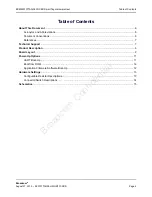
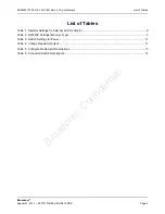
Page 3: ...t of Figures Figure 1 WICED Smart Tag4 Key Components 8 Figure 2 Board Assembly Top View 9 Figure 3 Board Assembly Bottom View 10 Figure 4 Baseband and PMU Schematics 15 Figure 5 RF Schematics 16 Figu...

Page 4: ...cronyms and Abbreviations 6 Document Conventions 6 References 7 Technical Support 7 Product Description 8 Board Layout 9 Power Up Options 11 UART Boot Up 11 Boot from ROM 12 Application Firmware Softw...

Page 5: ...List of Tables Table 1 Resistor Settings for External 32 KHz Crystal 9 Table 2 SW8 DIP Settings Memory Type 9 Table 3 Switch Settings for Power 11 Table 4 Voltage Regulator Output 11 Table 5 Configur...

Page 6: ...Smart devices Acronyms and Abbreviations In most cases acronyms and abbreviations are defined on first use For a comprehensive list of acronyms and other terms used in Broadcom documents go to http w...

Page 7: ...documentation schematic diagrams product bill of materials PCB layout information and software updates through its customer support portal For a CSP account contact your Broadcom Sales or Engineering...

Page 8: ...d 2 4 GHz transceivers The Broadcom WICED Smart Tag4 Figure 1 is an evaluation board that makes various pins on the BCM2073X available for debug evaluation and troubleshooting Figure 1 WICED Smart Tag...

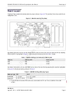
Page 9: ...lighted in Figure 2 above Resistor values are listed in Table 1 below By default the board is set to use EEPROM but can be set for serial flash by adjusting the resistors highlighted in Figure 2 to th...

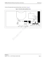
Page 10: ...5 920737TAG04 HWUM101 RDS Page 10 BCM920737TAG 04 WICED Smart Tag Hardware User Manual The Smart Tag evaluation board assembly bottom view is shown in Figure 3 Figure 3 Board Assembly Bottom View B r...

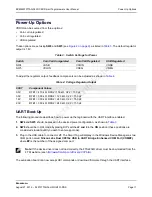
Page 11: ...sitions are considered standard until you wish to enter app mode 3 Plug in the USB cable to connector J7 The Smart Tag will display in the Windows Device Manager as two COM ports named Silicon Labs Du...

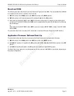
Page 12: ...ice is identified in the Windows Device Manager or Press and hold the BOOT ROM button SW1 press and release RESET SW3 release the BOOT ROM button SW1 The evaluation board can now accept HCI commands o...

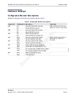
Page 13: ...C Internal DC DC converter RD6 A C External LDO DC DC converter B C Internal DC DC converter RD7 A C PCB monopole antenna B C External antenna connector J1 R26 Short External crystal 0 03277 MHz R26...

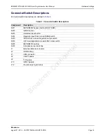
Page 14: ...ription SW1 EEPROM SF bypass button BOOT ROM SW2 GPIO0 button SW3 Hardware reset button SW4 Regulator input from coin cell USB switch SW5 VDDIO from coin cell regulator output switch SW6 HCI mode appl...

Page 15: ...2 5 P32 P8 P33 P1 2 5 P3 5 P14 P38 2 5 P24 P25 P32 SCL_SCK SDA_SI R7 1K LS1 PKLCS1212E4001 R1 C2 0 1uF Q1 2SC2712 Y LF MX25U4033EM1I 12G U3 SO8_1 27mm GND 4 SCLK 6 CS_L 1 VCC 8 WP_L SIO2 3 HOLD_L SIO...

Page 16: ...VRF LDOext LDOint LDOint LDOext EXT_LDO_IN EXT_LDO_IN P12 P26 2 5 P11 P27 2 5 R25 0 R26 0 DNI C9 1uF C15 1 8pF C21 12pF RD6 0 INSTALL POSITION B A B C U2B BCM20737A1KML2G QFN32H_0 5mm VDDFE 5 VDDVCO 7...

Page 17: ...X UP_TX UP_TX UP_RX P24 P25 PBC04SAAN J9 1 2 3 4 RFB1 360K RFB2 240K D7 10V C29 0 1uF R59 0 S M 100 2X9 J10 1 3 5 7 9 11 13 15 17 2 4 6 8 10 12 14 16 18 PBC04SAAN J2 1 2 3 4 C22 150pF R62 0 DNI FB3 60...

Page 18: ...CS 6 SDA SDI SDO 4 SDO SA0 5 INT DRDY 7 GND 9 GND 8 C59 0 1uF TP5 TP13 R65 10K U16 LIS3MDLTR LGA12_0 5mm VDD 5 RESVD_GND 2 INT 7 VDD_IO 6 SCL SPC 1 CS 10 SDA SDI SDO 11 SDO SA1 9 DRDY 8 RESVD_GND 12 G...

Page 19: ...any products or data herein to improve reliability function or design Information furnished by Broadcom Corporation is believed to be accurate and reliable However Broadcom Corporation does not assume...

Reviews: