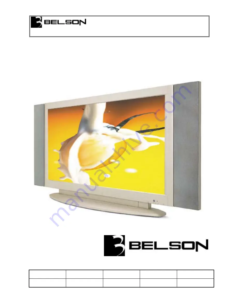
background image


SERVICE MANUAL (BSV-4251 BSV-4251A ) 

MODEL NAME 

DOCUMENT NO 

REVISION NO   REVISION DATE 

PAGE 


Service Manual   


BSV-4251/4251A RD(1) 

00 

03/10/23 

1/75 


Summary of Contents for BSV-4251

Page 1: ...SERVICE MANUAL BSV 4251 BSV 4251A MODEL NAME DOCUMENT NO REVISION NO REVISION DATE PAGE Service Manual BSV 4251 4251A RD 1 00 03 10 23 1 75...

Page 2: ...DISPLAY CELL DEFECT SPECIFICATION 12 BLOCK WIRING DIAGRAM 14 MODULE FUNCTION DEFINITION 16 MODULE BASIC CONFIGURATION 17 VSC BOARD PIN CONFIGURATION 18 OSD MENU FACTORY 21 DESCRIPTION OF VSC FUNCTIONS...

Page 3: ...G TROUBLESHOOTING 53 IMAGE STICKING CHARACTERISTICS 64 ISM MODE 66 SCHEMATIC PRINTED CIRCUIT BOARD EXPLODE VIEW 67 EXPLODED VIEW PARTS LIST 69 REPLACMENT PARTS LIST 71 EXPLODE VIEW 75 BSV 4251 4251A R...

Page 4: ...P42V51000 51300 YBT 51330 new ASIC LGE 5 Speaker Impedance 8 6 Sound Output 10W 10W 7 Feature AV Input Bottom Component1 Input Bottom DVD Component2 Input Bottom DTV D SUB Bottom RGB 15 pin S Video In...

Page 5: ...6 0 7 0 8 Vpp 2 COMPONENT Mode Y Cb Pb Cr Pr RESOLUTION H Freq KHz V Freq Hz Proposed 720 480 15 73 60 00 SDTV DVD 480I 720 576 15 63 50 00 SDTV DVD 576I 720 480 31 47 59 94 SDTV 480P 1280 720 45 00...

Page 6: ...L NAME DOCUMENT NO REVISION NO REVISION DATE PAGE Pin No Pin Name Spec Pin No Pin Name Spec 1 DCD NC 6 DSR NC 2 RXD 12 Vpp 7 RTS NC 3 TXD 12 Vpp 8 CTS NC 4 DTR NC 9 R NC 5 GND GND CONTROL DESCRIPTIONS...

Page 7: ...SERVICE MANUAL BSV 4251 BSV 4251A MODEL NAME DOCUMENT NO REVISION NO REVISION DATE PAGE BSV 4251 4251A RD 1 00 03 10 23 7 75...

Page 8: ...SERVICE MANUAL BSV 4251 BSV 4251A MODEL NAME DOCUMENT NO REVISION NO REVISION DATE PAGE OPTIONAL EXTRAS BSV 4251 4251A RD 1 00 03 10 23 8 75...

Page 9: ...extras can be changed or modified for quality improvement without notification new optional extras can be added Contract your dealer for buying these items REMOTE CONTROL BUTTONS When using the remote...

Page 10: ...SERVICE MANUAL BSV 4251 BSV 4251A MODEL NAME DOCUMENT NO REVISION NO REVISION DATE PAGE TELETEXT FUNCTION BSV 4251 4251A RD 1 00 03 10 23 10 75...

Page 11: ...SERVICE MANUAL BSV 4251 BSV 4251A MODEL NAME DOCUMENT NO REVISION NO REVISION DATE PAGE DISPLAY CELL DEFECT SPECIFICATION BSV 4251 4251A RD 1 00 03 10 23 11 75...

Page 12: ...SERVICE MANUAL BSV 4251 BSV 4251A MODEL NAME DOCUMENT NO REVISION NO REVISION DATE PAGE PDP42V51000 51300 51330 DEFINITION OF CELL DEFECT ZONE BSV 4251 4251A RD 1 00 03 10 23 12 75...

Page 13: ...SERVICE MANUAL BSV 4251 BSV 4251A MODEL NAME DOCUMENT NO REVISION NO REVISION DATE PAGE 1 Definition of Cell defect Zone 2 Display Dot Diagram BSV 4251 4251A RD 1 00 03 10 23 13 75...

Page 14: ...2 GB 80 000MHz FSDQM 7 0 FSDATA 63 0 A 21 0 D 7 0 I O EXTENDER SST39VF080AT FLASH HY62U8200 RAM 24LC16 EEPROM VCC12 AP1501 50 VCC5A AP1501 50 VCC5D VCC9 RC1117 VCC3 12V 12V 12V 12V Y Pb Pr R G B H V 5...

Page 15: ...SERVICE MANUAL BSV 4251 BSV 4251A MODEL NAME DOCUMENT NO REVISION NO REVISION DATE PAGE BSV 4251 4251A RD 1 00 03 10 23 15 75...

Page 16: ...utside DC DC 2 Board Distribution to X Y Z board after conversion from input voltage of Vs Va Voc to circuit logic voltage 5V FPC Flexible Plate Circuit The pattern connection of PCB and panel COF Chi...

Page 17: ...SERVICE MANUAL BSV 4251 BSV 4251A MODEL NAME DOCUMENT NO REVISION NO REVISION DATE PAGE MODULE BASIC CONFIGURATION PDP42V51000 51300 51330 BSV 4251 4251A RD 1 00 03 10 23 17 75...

Page 18: ...power breakdown 3 5V STBY I 5V 5V INPUT PORT FOR VSC STANDBY 2 RL ON O 5V 0V RELAY CONTROL PORT FOR POWER ON Relay On High Relay off Low 6 5V MNT I 5V 0V PDP MODULE STABLE CHECK PORT The port to provi...

Page 19: ...V 1 VCC5 I 5V 5V Input 2 VCC5 I 5V 5V Input 3 SCART_R I 0 7Vpp 0 1pp SCART RED INPUT PORT 4 SCART_G I 0 7Vpp 0 1pp SCART GREEN INPUT PORT 5 SCART_B I 0 7Vpp 0 1pp SCART BLUE INPUT PORT 6 SCART_FB I 1V...

Page 20: ...3dB SCART2 AUDIO RIGHT OUTPUT PORT 7 GND 0V 8 AFT I 9 GND 0V 10 TUNER_SIF I 11 GND 0V 12 TUNER_CVBS I 1 0Vpp 3dB TV VIDEO INPUT PORT 13 GND 0V 14 SDA3 I 5V 0V DATA LINE 15 SCL3 I 5V 0V CLOCK LINE 16 G...

Page 21: ...scaler input port CH1 or CH2 5 VPC3230 MAIN Value adjustment for video decoder s brightness and contrast color tickness in the main window 6 VPC3230 SUB Value adjustment for video decoder s brightness...

Page 22: ...E PAGE CALIBRATION MENU 1 PC Calibration Automatic adjustment as the fittest status of white balance for analogue input PC 2 DTV Calibration Automatic adjustment as the fittest status of white balance...

Page 23: ...uality improv ement fuction when TV input signal is weak Blue Screen When there are no input signal of the TV and external equipment you can install the screen color as blue Melody Volume Installation...

Page 24: ...justment of current screen Adjustment value of brightness for User Menu TTX Bright It is not useful mode Sub Contrast Contrast adjustment of scaler generating power Red Green Blue Gain Contrast adjust...

Page 25: ...tment of each Red Green Blue for scaler input port CH1 OR CH2 Red Green Blue Offset The brightness adjustment of each Red Green Blue for scaler input port CH1 OR CH2 APL Pixel Shift Pixel Number Time...

Page 26: ...sense adjustment of Composite S Video form s signal SATCb The blue color sense adjustment of Component RGB form s signal SATCr The red color sense adjustment of Component RGB form s signal CIPTNT The...

Page 27: ...color sense adjustment of Composite S Video form s signal SATCb The blue color sense adjustment of Component RGB form s signal SATCr The red color sense adjustment of Component RGB form s signal CIPT...

Page 28: ...ntrol dc offset Brightness of each respective channel Current Installation of PLL Part VCO Current For test VCO Installation of PLL Part VCO Range For test Pr Y Pb Gain Contrast adjustment of Componen...

Page 29: ...pattern as a certain time interval 2 Luma Ramp 16 Step It is gray pattern of 16 Step 3 Luma Ramp 128 Step It is gray pattern of 128 Step 4 White 16 It is low Gray pattern 5 White 240 It is high gray...

Page 30: ...VISION DATE PAGE VERSION MENU Version It is to show the Firmware Version Release It is to show the date of Firmware revision Panel Used Time It is to show the used time of Panel Panel Name It is to sh...

Page 31: ...tion of initial language of the TTX 2 Video Video format per country and it is composed of Normal NTSC PAL N M 3 Protocol Installation of communication protocol for remote control 4 LOGO Installation...

Page 32: ...within the outer perimeter of the screen without expanding the central area PIP Picture In Picture Function to enable the simultaneous viewing of two pictures by displaying a small sub frame within t...

Page 33: ...ound levels from each individual broadcasting company to an appropriate volume in case of watching a television connected to external equipment This allows to viewer to enjoy a comfortable and stable...

Page 34: ...t 480i or the like to Y UV digital pictures Compatible with various TV formats of NTSC PAL SECAM etc U41 VPC323OD _ 28_S LLC1 U42 LM2937 3 3V _ 3_V3 3 LC18 STS104B _ 2_VAA3230 U40 LM2937 3 3V _ 3_V3 3...

Page 35: ...V 4251A LC16 STS104B _ 2_VAA3230_1 U41 VPC3230D _ 28_VID_CLK U41 VPC3230D _ 53_INTLC U41 VPC3230D _ 57_VID VS U41 VPC3230D _ 56_VID HS MODEL NAME DOCUMENT NO REVISION NO REVISION DATE PAGE BSV 4251 42...

Page 36: ...an analog RGB signal to a process able digital signal Converts a component signal 480p 720p 1080i to a digital signal and transmits it to PW565 Scaler U2 AD9883 _ 30_ Hsync0 U2 AD9883 _ 31_Vsync0 U2 A...

Page 37: ...SERVICE MANUAL BSV 4251 BSV 4251A U1 LM2937 _ 3_ VO PW565 Scaler MODEL NAME DOCUMENT NO REVISION NO REVISION DATE PAGE BSV 4251 4251A RD 1 00 03 10 23 37 75...

Page 38: ...51 adjusted to a PDP display and transmitted to a PDP module In particular it receives any PC signal input at various scanning rates and performs scaling to adjust to PDP resolution RP12 R ARRAY _ 1_D...

Page 39: ...gnal out of many audio input signal options and produces a woofer signal or Headphone signal as well as a general Speaker signal LCD TV U45 MSP3450 _ 65_AVSUP U43 KIA7808AF _ 3_8V Output U45 MSP3450 _...

Page 40: ...STS104B _ 2_C344_5VST LC21 STS104B _ 2_C353_5VDD U15 RC1117_3 3V _ 2_VCC3 L10 33uH _ 2_R410_VCC12 Q33 MMBT3904 _ C _RL_ON Q30 MMBT3904 _ C _VAVS_ON MODEL NAME DOCUMENT NO REVISION NO REVISION DATE PAG...

Page 41: ...ATE PAGE MODULE SUPPLY VOLTAGE SEQUENCE PDP42V5 Life Expectancy The anticipated life time is estimated more than 25 000 hours of continuous operations Average life time is the time when the brightness...

Page 42: ...r Relay On 2 Continue 5Volt Monitoring If there is no 5Volt more than 10 minutes then power Off 3 Check if it is OK the 5Volt Mnt first And then VaVs On after 3 seconds 4 VaVs On waiting 3 seconds Dis...

Page 43: ...SERVICE MANUAL BSV 4251 BSV 4251A MODEL NAME DOCUMENT NO REVISION NO REVISION DATE PAGE PSU POWER SEQUENCE POWER DGK 420W BSV 4251 4251A RD 1 00 03 10 23 43 75...

Page 44: ...Voltage of D M M adjustment as same as Va voltage which on Label of panel right bottom Deviation 0 5V 1 1 2 Vs Adjustment Connect pin 1 3 of CN806 to jack of D M M After turning the VR3 Vs Adj voltag...

Page 45: ...SERVICE MANUAL BSV 4251 BSV 4251A MODEL NAME DOCUMENT NO REVISION NO REVISION DATE PAGE BSV 4251 4251A RD 1 00 03 10 23 45 75...

Page 46: ...movement to 2 color control on Factory Mode2 move to sub menu as choice of volume button 3 After check the Brightness 50 Contrast 90 choose the Sub Brightn ess 4 Zero calibration s execution of CA 100...

Page 47: ...tern of above picture Timing 395 Pattem 251 Reverse 720P 60Hz 2 After movement to 1 calibration on Factory Mode move to sub menu as choice of volume button 3 After movement to 2 DTV Calibration choose...

Page 48: ...fter movement to 1 calibration on Factory Mode move to sub menu as choice of volume button 3 After movement to 2 PC Calibration choose it with volume button 4 If Enter key it starts the calibration au...

Page 49: ...the product immediately turn off the power Continuing to use the product it is may cause fire or electric shock 4 If the product emits smoke and abnormal smell or makes an abnormal sound immediately...

Page 50: ...e power and disconnect all the cables While moving the product watch your step The product may be dropped or all leading to injuries of electric shock 10 In order to protect static electricity due to...

Page 51: ...product with a cloth or other covering while power is supplied to the product 23 Before turning on power to the product check the wiring of the product and confirm that the supply voltage is within t...

Page 52: ...SERVICE MANUAL BSV 4251 BSV 4251A MODEL NAME DOCUMENT NO REVISION NO REVISION DATE PAGE BSV 4251 4251A RD 1 00 03 10 23 52 75...

Page 53: ...Display X B D C A screen doesn if display at all and c 1 Check whether the CTRL B D LED D1 D4 is turned on or not 3 X B D Y B D Z B D is well plugged in 4 Check the connection of X B D Y B D and Z B...

Page 54: ...n is not be shown as data COF ing Example of the screen display form Anything of the 7 Data COF can be shown beside below pictures The problem between Data COF and X B D is more possible th 2 Confirm...

Page 55: ...check a COF connector D 3 I connected from CTRL to X B D D or CTRL B D Screen Display Form 1 In case of generating unusual pattern of Data COF IC unit as belo that is input into Data COF IC 2 In case...

Page 56: ...f one Data COF IC there is problem at the output of outputflatworm of X B D 2 C 3 R elationship between screen and X B D In case of generating regular stripe about the quantity of two Data COF IC that...

Page 57: ...Right Bottom reen 3 7 Lef D of the Sc t X B Screen Display Form 2 5 The screen display has a problem for Scan FFC 1 It s may be a problem between Scan FFC and Y B D 2 Check the connection of Y B D an...

Page 58: ...N DATE PAGE 6 The screen has a vertical line with regular gap A vertical stripe flash at especial color 2 1 This is a problem about control B D 2 Replace Control B D Screen Display Form 2 7 A data cop...

Page 59: ...een has one or several vertical line X B D COF FPC attached panel COF attached panel 3 R 1 In this case It isn t a problem about controller B D or 2 It may cause followings It s out of order a panel O...

Page 60: ...h below F G s s declination by changing VR1 VR2 VR3 k 1 In this case Z B D operation isn t complete 3 Check the connector of Z B D and Controller 4 Replace the Controller B D or Z B 2 1 The screen dis...

Page 61: ...VISION NO REVISION DATE PAGE 3 Replace the Z B D 13 It doesn t display a specified brightness at specified color 2 Replace the CTRL B D 1 No Power 2 1 Check the connector of CTRL B D input signal 3 No...

Page 62: ...connective condition and various connect or Connect plug with the set Check OPEN With CN806 CN13 C IC1 rt heck the Vs Voltage 5 IC16 PSU Pa and VSC Part Q30 Short Check AC Line Fuse Replace IC15 IC16...

Page 63: ...nn Input PC DTV Signal Input DV D Signal Input Tuner CVB S CVBS F H SCART S Video Signal Input F SCART RGB Signal Check BA7657 U8 Check AD9883 U2 Check Cable Abnormal Normal Normal Check MSP3450G U45...

Page 64: ...seen with the naked eyes ecular change average Conditions All white 100 white input at an ambient temperature of 25 However this lifetime is n the data for refernce arrenty 4 Cause of deterioration in...

Page 65: ...ted n colored ground mixture of R G B recommended ISM Mode Image Sticking Minimization Mode Apart from the above proposal This module has been equipped with a special method that minimizes the image s...

Page 66: ...ts initial value at the white window pattern 1 25 of full white pattern change of APL Data is no less than 4 and it will remain for more than 5 less of time it will not operate where the display load...

Page 67: ...SERVICE MANUAL BSV 4251 BSV 4251A MODEL NAME DOCUMENT NO REVISION NO REVISION DATE PAGE PSU DGK 420W BOTTOM BSV 4251 4251A RD 1 00 03 10 23 67 75...

Page 68: ...SERVICE MANUAL BSV 4251 BSV 4251A MODEL NAME DOCUMENT NO REVISION NO REVISION DATE PAGE EXPLODED VIEW PARTS LIST No Part no Description BSV 4251 4251A RD 1 00 03 10 23 68 75...

Page 69: ...EY 1 S150111021 PACKING ASSY EPT 4200A PAL 2 S15012F021 ACCESSORY ASSY EPT 4200A PAL 3 S15013C021 REMOCON ASSY EPT 4200A PAL 3 71BELP324 JACK HOUSING AL PAL TV 3 71BELP315 HEAT SHINK AL 28X28X13 4 71B...

Page 70: ...WASHER 8 2 74GELM008 GRAOUND SCREW PH M 4X10 SPECIAL 3 76AZW15D42D15 WASHER SPCC 15X4 2X1 5T ZW 2 50 0007 WIRE ASSY AUDIO OUT 4P EPM 420 2 50 0074 WIRE ASSY AUDIO POWER 4P 250mm 2 50 0075 WIRE ASSY A...

Page 71: ...230D C5 PQFP 80 4 01 0259 IC FDC6561AN Super SOT 6 4 01 0260 IC MSP3450G PQFT 80 4 01 0261 IC SST39VF080AT TSOP40 4 01 0262 IC SDA5550 M 3901 A14 9RF 4 01 0263 IC HY62U8200BLLST 85I sTSOP 4 01 0264 IC...

Page 72: ...1608 TP 4 10 0189 CC CHIP 25V 105Z 1608 TP 4 10 0197 CC CHIP 25V 682J 1608 TP 5 10 0004 CC CHIP 25V 101J 1608 TP 5 10 0016 CC CHIP 16V 224Z 1608 TP 5 10 0021 CC CHIP 25V 102K 1608 TP 10 0022 CC CHIP...

Page 73: ...IAL 2 17 0011 CORE ZCAT 1518 0730 M K 4 17 0003 BEAD HB 1M2012 221JT 4 17 0004 BEAD HH 1M3216 121JT 4 17 0016 BEAD HB 1M2012 121JT 4 17 0023 BEAD HCB 4516K 600T60 4 17 0023 BEAD HCB 4516K 600T60 5 17...

Page 74: ...14 0476 R CHIP 1608 474F TP 4 14 0008 R CHIP 1608 101F TP 4 14 0010 R CHIP 1608 102F TP 4 14 0012 R CHIP 1608 103F TP 4 14 0052 R CHIP 1608 472F TP 4 14 0055 R CHIP 1608 473J TP 4 14 0069 R CHIP 1608...

Page 75: ...SERVICE MANUAL BSV 4251 BSV 4251A EXPLODE VIEW MODEL NAME DOCUMENT NO REVISION NO REVISION DATE PAGE BSV 4251 4251A RD 1 00 03 10 23 75 75...

Reviews: