Access from the user program
KL3311, KL3312, KL3314 and KL3302
43
Version: 4.2
•
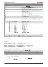
R34: User scaling - gain (A_w)
16-bit signed integer*2
-8
This register contains the scaling factor of the user linear equation (
•
R35 and R36: reserved
•
R37: Filter constant
[0x0000]
Applies to all terminals from firmware version 3x.
This documentation applies to all terminals from firmware version 3x. The version information can
be found on the right-hand side of the terminal in the serial number: xxxx3xxx.
Example: 5298
3A
2A => the firmware version is
3A
.
Filter constant
First notch [Hz]
Conversion time [ms]
0x0000
25
250
0x50
100
65
0xA0
50
125
0x140
25
250
0x280
12.5
500
5.5
Control and status byte
Control byte for process data exchange
The control byte is transferred from the controller to the terminal. The control byte is not used for KL331x and
KL3302.
Status byte for process data exchange
The status byte is transmitted from the controller to the terminal. It contains various status bits of the analog
input channel:
Status byte:
Bit 7 = 0
bin
Bit 6 = 1
bin
:
Error (general error bit)
Bit 5 to bit 2:
reserved
Bit 1 = 1
bin
:
Overrange
Bit 0 = 1
bin
:
Underrange
Compensation
The terminals are compensated when delivered.
In order to compensate tolerances of the external components, gain and offset registers for compensating
the thermocouple voltage are implemented for each channel, i.e. R17 (thermocouple voltage offset) and R18
(thermocouple voltage gain). For compensating the cold junction temperature (temperature at the transition
between the thermocouple and the terminal contacts), a gain register (R21) is implemented, which is
identical for both sets of registers.
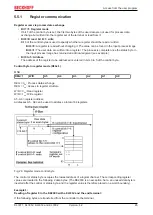
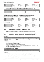
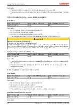
Compensation can be carried out as follows:
First of all the offset calibration is carried out with 0 V input voltage, reference temperature deactivated and
linearization switched off. 0xF100 is entered in the feature register.
This is followed by gain compensation with a maximum voltage of 125 mV (typical value: 70 mV). With this
terminal setting with vendor scaling deactivated, the voltage is output in 4 µV per digit.
Gain and offset compensation of the thermocouple voltage is carried out separately for each channel.


