103
ATmega103(L)
0945G–09/01
E: Load Data High Byte.
1.
Set BS1 to “1”. This selects high data.
2.
Set XA1, XA0 to “01”. This enables data loading.
3.
Set DATA = Data high byte ($00 - $FF).
4.
Give XTAL1 a positive pulse. This loads the data high byte.
F: Latch Data High Byte.
1. Give PAGEL a positive pulse. This latches the data high byte.
G: Repeat B through F 128 times to fill the page buffer.
H: Load Address High Byte.
1.
Set XA1, XA0 to “00”. This enables address loading.
2.
Set BS1 to “1”. This selects high address.
3.
Set DATA = Address high byte ($00 - $FF).
4.
Give XTAL1 a positive pulse. This loads the address high byte.
I: Program Page.
1.
Give WR a negative pulse. This starts programming of the entire page of data.
RDY/BSY goes low.
2.
Wait until RDY/BSY goes high.
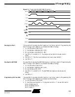
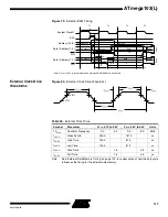
(See Figure 74 for signal waveforms.)
J: End Page Programming.
1.
Set XA1, XA0 to “10”. This enables command loading.
2.
Set DATA = “0000 0000”. This is the command for No Operation.
3.
Give XTAL1 a positive pulse. This loads the command and the internal write sig-
nals are reset.
K: Repeat A through J 512 times or until all data has been programmed.
Figure 73.
Programming the Flash Waveforms
$10
ADDR. LOW
ADDR. HIGH
DAT
A LOW
DATA
XA1
XA2
BS1
XTAL1
RDY/BSY
RESET
WR
OE
+12V
BS2
PAGEL

