


Related information
2.18 System debug
1.3 Location of components on the MPS3 board
A.1.2
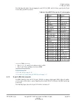
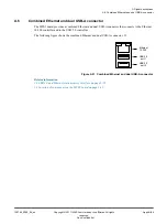
10-pin IDC connector
The MPS3 board provides one 1V8 10
‑
pin IDC connector that supports P
‑
JTAG processor debug to
enable connection of DSTREAM or a compatible third
‑
party debugger. The connector also supports
Serial Wire Debug
(SWD).
The 10
‑
pin IDC connector connects to general
‑
purpose pins on the FPGA. The availability of P
‑
JTAG or
SWD depends on the design that you implement in the FPGA.
The following figure shows the 10
‑
pin IDC connector, J15.
1
9
2
10
Figure A-2 10-pin IDC connector
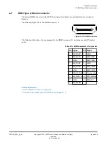
The following table shows the pin mapping for each P
‑
JTAG and SWD signal on the 10
‑
pin IDC
connector.
Table A-2 10-pin IDC connector, J15, pin mapping
Pin Signal
Pin Signal
1
1V8
2
SWDIO
/
TMS
3
GND
4
SWDCLK
/
TCK
5
GND
6
SWO
/
TDO
7
NC
8
NC/
TDI
9
GNDDETECT
10
nSRST
Note
• Pins 2, 6, 8, and 10 have pullup resistors to
1V8
.
• Pin 4 has a pulldown resistor to
GND
.
Related information
2.18 System debug
1.3 Location of components on the MPS3 board
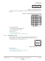
A.1.3
20-pin Cortex debug and ETM connector
The MPS3 board provides one 1V8 20
‑
pin Cortex debug and
Embedded Trace Macrocell
(ETM)
connector. The connector supports P
‑
JTAG processor debug to enable connection of DSTREAM, or a
compatible third
‑
party debugger. The connector also supports
Serial Wire Debug
(SWD) and 4
‑
bit trace.
The 20
‑
pin Cortex debug and ETM connector connects to general
‑
purpose pins on the FPGA. The
availability of P
‑
JTAG, SWD, or 4
‑
bit trace depends on the design that you implement in the FPGA.
The following figure shows the 20
‑
pin Cortex debug and ETM connector, J12.
A Signal descriptions
A.1 Debug connectors
100765_0000_04_en
Copyright © 2017–2020 Arm Limited or its affiliates. All rights
reserved.
Appx-A-72
Non-Confidential