


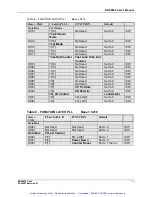


DBS9900 User’s Manual
7-16
DBS9900 Clock
82-28993 Revision 01
7.9.1
TIME BASE CLOCK Inputs
REFSEL
is a signal output that controls a 2:1 mux to select either External or Internal Reference
Oscillators. REFSEL should be set high when External Reference is selected and PLL_EN is
asserted. See section
Error! Reference source not found.
for truth table.
PLL_EN
is a control output that enables the VCO and PLL Integration Amplifier. This is used
when the PLL is to be used with either External or Internal Reference Oscillators. This line is
decoded in Software. See section
Error! Reference source not found.
for truth table.
INTREF
is a signal that enables the Internal Reference Oscillator.
INTREF
should be asserted
when
PLL_EN
is asserted and Internal reference oscillator is to be used. See section
Error!
Reference source not found.
for truth table.
FREQSEL[1:0]
is decoded according to the following table.
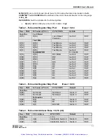
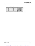
Table 20 - D[09:08] Frequency Select Truth Table
TB CONTROL
D[09:08]
FREQSEL[1:0]
11
HSDIV_EN
Enables HSDIV divider
10
HSDIV2_EN
Enables HSDIV FF
01
LSDIV_EN
Enables LSDIV
00
No Clock
Disable Time Base Clock
(Default)
When
FREQSEL[1:0] = 0h
the time base selects no clock. Under this condition,
PLL_EN,
INTREF
should be disabled and
REFSEL
should be set low.
When
FREQSEL[1:0]
=
1h, PLL_EN
should be enabled and
REFSEL
and
INTREF
should be
asserted depending on whether internal or external reference oscillator is to be used. The
HSDIV
divider should be programmed to
HSDIV[3:0] = 7h
(divide ratio of 8).
LSDIV
can be programmed
to modify the output clock frequency with divide ratios of 32 to 1,048,592, in steps of 16
(95.36598Hz to 6.25MHz frequency range).
When
FREQSEL[1:0]
=
2h
,
PLL_EN
should be enabled along with either external or internal
oscillator and the
HSDIV
divider can be programmed to modify the output clock frequency with
divide ratios of 4 to 32, in steps of 2 (3.125MHz to 50MHz frequency range).
When
FREQSEL[1:0]
is set to
3h
,
PLL_EN
should be enabled along with either external or
internal oscillator. The
HSDIV
divider should be programmed to
1h
(divide ratio of 2) to modify the
output clock frequency with divide ratio of 2 (50MHz to 100MHz frequency range).
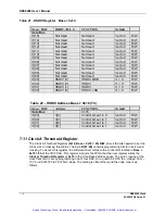
7.9.2
D[07:05] MISCELANEOUS Control bits
When
UP_DOWN
D[07]
is set high, and
CS
D[06]
is set high, the EEPROM
Spur trim pot
will
advance it’s wiper towards the high rail (+2.5V + .25V) of the trim pot on the rising edge of
INC
.
This increases compensation current applied to the PLL loop amplifiers negative input to a
maximum of +100nA. When
UP_DOWN
D[07]
is set low and
CS
D[06]
is set high, the EEPROM
Spur trim pot
will advance it’s wiper towards the low rail (+2.5V - .25V) of the trim pot on the
rising edge of
INC D[05]
. This decreases compensation current to a minimum of -100nA. This
compensation current acts to null mismatch between source/sink current output of the PLL
charge pump. This in turn nulls out the frequency spurs located at offset frequencies spaced
Fpd
apart around the PLL carrier frequency (
Fvco
).
Artisan Technology Group - Quality Instrumentation ... Guaranteed | (888) 88-SOURCE | www.artisantg.com