UG-669
EVAL-ADuC7026 User Guide
Rev. B | Page 8 of 16
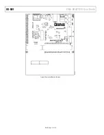
EXTERNAL MEMORY INTERFACE
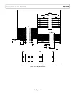
A footprint for a 32 k × 16 SRAM, a 64 k × 16 flash, and a
16-bit D-latch are provided on board because address and data
are multiplexed on the external bus.
The memory footprints are for a CY7C1020CV33 and
AT29LV1024. The latch footprint is for a 74LVT16373AGG.
Note that you can use different versions of the CY7C1020CV33
memory, with different access times. Wait states can be added in
the XMxPAR register to allow for interfacing to slower memory,
if required.
CONNECTIONS
Table 4.
Connection
Description
Controls
RS, WS, and AE are the minimum control signals of any memory interface.
MS0 and MS1, memory select signals, are connected to the CE of the SRAM and the flash, respectively, to enable the
memory when necessary.
BHE and BLE allows the high or low byte of the 16-bit SRAM to be selected.
Data
16 bits of address data, (AD[15:0]), are directly connected from the
to the memory circuitry.
Addresses
16 bits of address IO[16:1] are connected from the
to AD[15:0] of the memory devices. AD[0] addresses a byte.
To address the 32 k of the SRAM only, 14-bit addresses are required.
15-bit addresses are required for the 64 k flash.


