Analog Devices EVAL-ADPD144RI User Manual Download Page 6

UG-1272 

EVAL-ADPD144RIZ-SF

 User Guide


Rev. 0 | Page 6 of 10 

EVALUATION BOARD SCHEMATICS AND ARTWORK 


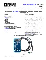
Figure 9. EVAL-ADPD144RIZ-SF BR-048862 Schematic 

CO

NNEC

T

O

R

 1

 (F

R

O

M

 DAU

G

H

T

E

R

)

C

O

NNEC

T

O

R

 1

 (T

O

 D

AUG

H

T

ER)

3.

3V

PB0

 (

SEL)

1.

8V

IN

T

ADJ

_

V

DD

EEPRO

M

 M

EM

O

R

Y

P

B1

 (A

CC)

SAM

E

 NAM

ES 

AS 

G

LUE 

M

O

THERB

O

ARD

D

F

4

0

C

-2

0D

P

-0.

4

V

(5

1)

D

F

4

0

C

-2

0D

P

-0.

4

V

(5

1)

D

F

40

C

-20D

P

-0.

4V

(51)

3P

IN

_JU

M

P

E

R

FTS

H

-10

8-

01

-L

-D

-K

0Ω

3P

IN

_J

U

M

P

E

R

TB

D

080

5

0Ω

TB

D

0805

0Ω

0Ω

TB

D

0805

TB

D

0805

0Ω

0

0

DN

I

DN

I

0Ω

3P

IN

_J

U

M

P

E

R

0Ω

0Ω

0Ω

0Ω

0Ω

0Ω

0Ω

0Ω

0Ω

0Ω

0Ω

0Ω

0Ω

0Ω

TS

W

-11

0-

08

-G

-D

3P

IN

_JU

M

P

E

R

M

24C

16-

D

F

C

U

6T

P

/K

D

F

40

C

-20D

P

-0.

4V

(51)

3

P

IN

_J

UM

PER

D

F

40

C

-20D

P

-0.

4V

(51)

D

F

40

C

-20D

P

-0.

4V

(51)

F

T

S

H

-1

0

8

-0

1-L

-D

-K

PW

2

PW

3

PW

4

PW

6

JP

6

C6

C3

JP

4

C2

JP

3

C1

JP

2

PW

1

R3

0

P1

TP1

PR1

JP

8

JP

7

JP

9

JP

13

PR1

R2

7

PW

7

R1

4

R1

6

R1

8

R2

2

R2

4

R2

0

R1

3

R1

5

R1

7

R1

9

R2

1

R2

3

R2

5

R1

2

P1

JP

1

R2

9

R3

P3

P3

P2

P2

U1

0

CO

NN

1_

I2

C_

SDA/

P0

_5

CO

NN

1_

I2

C_

SCL

/P0

_

4

J_

CO

NN1

_T

M

R0

_

O

UT

/P

0

_1

4

J_

CO

NN1

_W

A

K

E0

/P

0_

1

5

J_

C

O

N

N

1

_S

P

I1

_

C

S

0

/P

1_

CO

NN

1_

SPI

1

_M

O

SI

/P

1

_7

CO

NN

1_

I2

C_

SCL

/P0

_

4

T_C

O

N

N

1_

W

A

K

E

1/

P

1_0

C

O

N

N

1_

I2C

_S

D

A

/P

0_5

RI

BBO

N_

INT

T

_

CO

NN

1_

W

AKE

0/

P0

_1

5

T

_CO

N

N1

_

T

M

R0

_

O

UT

/P

0

1

4

RI

BBO

N_

IN

T

T

_C

O

NN

1_

W

AKE1

/P1

_0

T_C

O

N

N

1_

S

P

I1_C

S

1

/R

TC

1_

O

P

C

1

/P

2_11

CO

N

N

1

_I

2

C_

SCL

/P0

_4

T_C

O

N

N

1_

TM

R

0_O

U

T

/P

014

T

_

CO

NN

1_

W

AKE

0/

P0

_1

5

T_C

O

N

N

1_

S

P

I1_C

S

0

/P

1_

9

C

O

N

N

1_

S

P

I1_M

O

S

I/P

1_7

VBO

O

ST

VO

U

T

_

C

O

N

1

VLDO

1

/IO

VDD

VLDO

1/

IO

VD

D

CO

NN1

_

SPI

1_

M

ISO

/P

1

_

8

CO

NN1

_

SPI

1_

CL

K/

P1

_

6

VBO

O

ST

VLDO

2

T_C

O

N

N

1_

S

P

I1_C

S

3

/P

1_10

C

O

N

N

1_

S

P

I1_M

O

S

I/P

1_7

RI

BB

O

N_

P

B1

RI

BB

O

N

_

P

B0

T

_C

O

NN1

_

W

AKE0

/P0

_1

5

VDD

_3

V

VBO

O

ST

VLDO

2

RI

BBO

N

_I

NT

RI

BBO

N

_P

B0

CO

N

N

1

_I

2

C_

SDA/

P0

_

5

C

O

N

N

1_

S

P

I1_C

LK

/P

1_

6

VLDO

2

VBO

O

ST

VL

DO

2

VLD0

3

M

B

_

V

L

D

O

1

/IO

V

D

D

MB

_V

L

D

O2

MB

_V

B

OOS

T

VLDO

2

V

B

OOS

T

VLDO

1

/IO

VDD

MB

_

V

L

D

O

1/IO

V

D

D

VO

UT_

C

O

N

1

MB

_

V

B

O

OS

T

CO

NN

1_

SPI

1

_C

L

K/

P1

_

6

MB

_

V

L

D

O

1/IO

V

D

D

MB

_

V

L

D

O

2

MB

_

V

B

O

OS

T

J_C

O

N

N

1_

S

P

I1_C

S

3/

P

1_10

J_C

O

N

N

1_

A

D

C

0_V

IN

1/

P

2_4

J_C

O

N

N

1_

S

P

I1_C

S

1/

P

2_11

J_

C

O

N

N

1

_WA

K

E

1

/P

1_

0

T_

C

O

N

N

1_

S

P

I1_

C

S

0/

P

1_9

T_C

O

N

N

1_

W

A

K

E

0/

P

0_1

5

T_

C

O

N

N

1_

S

P

I1_

C

S

3/

P

1_1

0

T_C

O

N

N

1_

S

P

I1_

C

S

0/

P

1_9

T

_

CO

NN

1_

AD

C0

_V

IN

1

/P2

_4

T_C

O

N

N

1_

W

A

K

E

0/

P

0_15

T

_

CO

NN1

_

SPI

1_

CS1

/RT

C1

_

O

PC1

/P2

_1

1

C

O

N

N

1_

S

P

I1_C

S

3/

P

1_10

CO

NN1

_S

PI

1

_

C

S0

/P

1_

9

CO

N

N1

_T

M

R0

_O

UT

/P

01

4

J_C

O

N

N

1_

S

P

I1_C

S

0/

P

1_9

J_

C

O

N

N

1_W

A

K

E

0/

P

0_

15

C

O

N

N

1_

W

A

K

E

1/

P

1_0

J_

CO

NN1

_

W

A

K

E1

/P

1_

0

C

O

N

N

1_

W

A

K

E

0/

P

0_1

5

T_C

O

N

N

1_

TM

R

0_O

U

T

/P

014

C

O

N

N

1_

S

P

I1_C

S

1

/R

TC

1_

O

P

C

1

/P

2_11

T

_

CO

NN1

_

W

AKE1

/P1

_

0

J_C

O

N

N

1_T

M

R

0_O

U

T

/P

0_

14

J_

CO

NN1

_

SPI

1_

CS3

/P1

_1

0

CO

NN

1_

SPI

1

_M

ISO

/P

1

_8

I2

C_

SDA/

P0

_

5

CO

NN

1_

I2

C_

SDA/

P0

_5

I2

C_

SCL/

P0

_

4

T

_

CO

N

N

1

_AD

C0

_V

IN

1/

P2

_

4

C

O

N

N

1_I

2C

_S

C

L

/P

0_4

RI

BB

O

N_

P

B1

RI

BB

O

N

_

P

B1

T

_

CO

NN1

_

SPI

1_

CS1

/RT

C1

_

O

PC1

/P2

_1

1

M

B

_V

LD

03

J_

CO

NN1

_

SPI

1_

CS1

/P2

_1

1

J

_C

O

NN1

_

ADC

0_

VI

N1

/P

2_

4

CO

N

N

1

_A

DC0

_V

IN

1/

P2

_

4

CO

N

N

1

_I

2

C_

SDA/

P0

_

5

C

O

N

N

1_T

M

R

0_O

U

T

/P

01

4

C

O

N

N

1_I

2C

_S

D

A

/P

0_5

C

O

N

N

1_I

2C

_S

C

L

/P

0_

VBO

O

ST

VLDO

1/

IO

VDD

VO

U

T

__

AC

T

C

O

N

N

1_W

A

K

E

0/

P

0_15

C

O

N

N

1_S

P

I1_C

S

0/

P

1_

9

C

O

N

N

1_S

P

I1_M

O

S

I/P

1_7

VLDO

1

/IO

VDD

VLDO

2

VLDO

2

VO

UT_

C

O

N

1

VO

UT

__

AC

T

CO

N

N

1

_I

2

C_

SCL

/P0

_4

CO

NN1

_

SPI

1_

M

ISO

/P

1

_

8

CO

NN1

_

SPI

1_

CS0

/P1

_9

C

O

N

N

1_

S

P

I1_C

S

3/

P

1_10

C

O

N

N

1_

A

D

C

0_V

IN

1/

P

2_4

C

O

N

N

1_

S

P

I1_M

IS

O

/P

1_8

C

O

N

N

1_

S

P

I1_C

LK

/P

1_

6

C

O

N

N

1_

S

P

I1_C

S

1

/R

TC

1_

O

P

C

1

/P

2_11

C

O

N

N

1_

W

A

K

E

1/

P

1_0

VBO

O

ST

2

4

6

8

10

12

14

16

18

20

1

3

5

7

9

11

13

15

17

1

3

5

7

9

11

13

15

17

19

2

4

6

8

10

12

14

16

18

20

1

20

19

18

17

16

15

14

13

11

10

8

7

6

5

4

3

2

9

12

15

13

11

9

7

5

3

1

16

14

12

10

8

6

4

2

4

2

6

8

10

12

14

16

18

20

1

3

5

7

9

11

13

15

17

19

19

SDA

SC

L

VSS

VCC

AG

ND

AG

N

D

AG

ND

AG

N

D

AG

ND

B

CO

M

A

B

CO

M

A

B

CO

M

A

B

CO

M

A

AG

N

D

AG

ND

AG

ND

AG

ND

AG

N

D

B

CO

M

A

16737

-017

Summary of Contents for EVAL-ADPD144RI

Page 1: ...g the ADPD144RI a complete photometric system designed to measure optical signals from ambient light and from synchronous reflected light emitting diode LED pulses The evaluation system includes the Applications Wavetool graphical user interface GUI which provides users with low level and high level configurability real time frequency and time domain analysis and a user datagram protocol UDP trans...

Page 2: ...ed 3 Installing the Applications Wavetool 3 Connecting the EVAL ADPDUCZ Microcontroller Board and the EVAL ADPD144RIZ SF 3 Checking the USB Serial Connection in Windows 3 Updating the EVAL ADPDDUCZ Firmware 3 Acquiring Data 4 Running the Applications Wavetool 4 USB UART Connection 4 Selecting the Proper View 4 Load Configuration 4 Optimizing and Running the ADPD144RI 5 Evaluation Board Schematics ...

Page 3: ... the EVAL ADPDUCZ the second LED near the power switch illuminates indicating that the on board battery is charging CHECKING THE USB SERIAL CONNECTION IN WINDOWS Ensure that the communications port COM port driver is installed correctly To verify proper installation go to Control Panel All Control Panel Items System Device Manager as shown in Figure 3 In this case the proper COM port choice is USB...

Page 4: ...re any other connection issues refer to the Applications Wavetool user guide that is provided in the software package download SELECTING THE PROPER VIEW The ADPD144RI is intended for nonwrist based PPG measurements Click the ADPD Device data view see Figure 6 to open a window that allows the user to run the ADPD144RI device and collect data see Figure 7 Figure 6 Click ADPD Device LOAD CONFIGURATIO...

Page 5: ...ttings can be optimized for any set of conditions by manipulating LED drive currents transimpedance amplifier TIA gain and analog front end AFE timing Another option is to use different operating modes that can be more optimal for a specific set of conditions such as using float mode for a low current transfer ratio CTR For information on optimization of the ADPD144RI refer to the ADPD144RI data s...

Page 6: ... VLD03 MB_VLDO1 IOVDD MB_VLDO2 MB_VBOOST VLDO2 VBOOST VLDO1 IOVDD MB_VLDO1 IOVDD VOUT_CON1 MB_VBOOST CONN1_SPI1_CLK P1_6 MB_VLDO1 IOVDD MB_VLDO2 MB_VBOOST J_CONN1_SPI1_CS3 P1_10 J_CONN1_ADC0_VIN1 P2_4 J_CONN1_SPI1_CS1 P2_11 J_CONN1_WAKE1 P1_0 T_CONN1_SPI1_CS0 P1_9 T_CONN1_WAKE0 P0_15 T_CONN1_SPI1_CS3 P1_10 T_CONN1_SPI1_CS0 P1_9 T_CONN1_ADC0_VIN1 P2_4 T_CONN1_WAKE0 P0_15 T_CONN1_SPI1_CS1 RTC1_OPC1 ...

Page 7: ...ADPD144RIZ SF BR 048911 Secondary Layer ADPD144RI ACEZ 10kΩ 1µF 1µF 10kΩ 0 01µF U1 C3 C4 C2 VLED VDD GND C1 1µF R2 R1 SCL SDA INT SCL INT SDA VLED SCL INT SDA SCL GND_LOCAL VDD VLED SDA GND_LOCAL VDD GND_LOCAL VDD GND_LOCAL GND_LOCAL 6 7 10 5 2 12 1 8 9 11 3 4 SPARE PIN SPARE PIN SCL INT VDD2 LED1 DNC LED2 DNC VLED VREF VDD1 AGND DGND SDA LGND 16737 018 16737 019 16737 021 ...

Page 8: ...UG 1272 EVAL ADPD144RIZ SF User Guide Rev 0 Page 8 of 10 Figure 13 EVAL ADPD144RIZ SF BR 048862 Primary Layer Figure 14 EVAL ADPD144RIZ SF BR 048862 Secondary Layer 16737 020 16737 022 ...

Page 9: ...EVAL ADPD144RIZ SF User Guide UG 1272 Rev 0 Page 9 of 10 Figure 15 EVAL ADPD144RIZ SF Connected to the EVAL ADPDUCZ Microcontroller Board 16737 100 ...

Page 10: ...he EvaluationBoard or termination of this Agreement Customer agrees to promptly return the Evaluation Board to ADI ADDITIONAL RESTRICTIONS Customer may not disassemble decompile or reverse engineer chips on the Evaluation Board Customer shall inform ADI of any occurred damages or any modifications or alterations it makes to the Evaluation Board including but not limited to soldering or any other a...

Reviews: