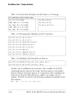
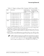
background image

Data Register File

2-38

ADSP-2126x SHARC Processor Hardware Reference


Data Register File

Each of the DSP’s processing elements has a data register file, which is a 
set of data registers that transfers data between the data buses and the 
computational units. These registers also provide local storage for oper-
ands and results.   

The two register files consist of 16 primary registers and 16 alternate (sec-
ondary) registers. All of the data registers are 40 bits wide. Within these 
registers, 32-bit data is always left-justified. If an operation specifies a 
32-bit data transfer to these 40-bit registers, the eight LSBs are ignored on 
register reads, and the LSBs are cleared to zeros on writes.

Program memory data accesses and data memory accesses to/from the reg-
ister file(s) occur on the PM data bus and DM data bus, respectively. One 
PM data bus access for each processing element and/or one DM data bus 
access for each processing element can occur in one cycle. Transfers 
between the register files and the DM or PM data buses can move up to 
64 bits of valid data on each bus.

If an operation specifies the same register file location as both an input 
and output, the read occurs in the first half of the cycle and the write in 
the second half. With this arrangement, the DSP uses the old data as the 
operand, before updating the location with the new result data. If writes 
to the same location take place in the same cycle, only the write with 
higher precedence actually occurs. The DSP determines precedence for 
the write operation from the source of the data; from highest to lowest, 
the precedence is:

1. Data memory or universal register (

Ureg

)

2. Program memory

3. PEx ALU

4. PEy ALU

Summary of Contents for ADSP-21261 SHARC

Page 1: ...P 2126x SHARC Processor Hardware Reference Includes ADSP 21261 ADSP 21262 ADSP 21266 ADSP 21267 Revision 5 1 April 2013 Part Number 82 002002 01 Analog Devices Inc One Technology Way Norwood Mass 02062 9106 ...

Page 2: ...e accurate and reliable However no responsibility is assumed by Analog Devices for its use nor for any infringement of patents or other rights of third parties which may result from its use No license is granted by impli cation or otherwise under the patent rights of Analog Devices Inc Trademark and Service Mark Notice The Analog Devices logo Blackfin SHARC TigerSHARC CrossCore VisualDSP and EZ KI...

Page 3: ...ce xxxi Manual Contents xxxii What s New in This Manual xxxiv Technical Support xxxiv Supported Processors xxxv Product Information xxxv Analog Devices Web Site xxxvi EngineerZone xxxvi Notation Conventions xxxvii Register Diagram Conventions xxxviii INTRODUCTION Design Advantages 1 1 Architectural Overview 1 4 ...

Page 4: ...ools 1 13 Differences From Previous SHARCs 1 14 Processor Core Enhancements 1 15 Processor Internal Bus Changes 1 15 Memory Organization Enhancements 1 16 Parallel Port Enhancements 1 16 I O Architecture Enhancements 1 16 Instruction Set Enhancements 1 16 PROCESSING ELEMENTS Numeric Formats 2 3 IEEE Single precision Floating point Data Format 2 4 Extended precision Floating Point Format 2 6 Short ...

Page 5: ...Arithmetic Logic Unit ALU 2 17 ALU Operation 2 17 ALU Saturation 2 18 ALU Status Flags 2 19 ALU Instruction Summary 2 20 Multiply Accumulator Multiplier 2 23 Multiplier Operation 2 23 Multiplier Result Register Fixed Point 2 24 Multiplier Status Flags 2 27 Multiplier Instruction Summary 2 28 Barrel Shifter Shifter 2 30 Shifter Operation 2 31 Shifter Status Flags 2 35 Shifter Instruction Summary 2 ...

Page 6: ...Operations 2 50 PROGRAM SEQUENCER Instruction Pipeline 3 4 Instruction Cache 3 5 Bus Conflicts 3 5 Block Conflicts 3 7 Using the Cache 3 8 Optimizing Cache Usage 3 9 Branches and Sequencing 3 11 Conditional Branches 3 12 Delayed Branches 3 13 Loop and Status Stacks and Sequencing 3 16 Conditional Sequencing 3 17 Core Stalls 3 21 Execution Stalls 3 23 DAG Stalls 3 24 Memory Stalls 3 24 IOP Register...

Page 7: ...onal Data Moves 3 38 Case 1 Complementary Register Pair Data Move 3 39 Example 1 Register to Memory Move PEx Explicit Register 3 39 Example 2 Register Move PEy Explicit Register 3 40 Example 3 Register to Memory Move PEx Explicit Register 3 40 Example 4 Register to Memory Move PEy Explicit Register 3 41 Case 2 Uncomplimentary to Complementary Register Move 3 42 Example Register Moves Uncomplimenta...

Page 8: ...imer and Sequencing 3 46 Interrupts and Sequencing 3 48 Delayed Interrupt Processing 3 52 Sensing Interrupts 3 53 Masking Interrupts 3 54 Latching Interrupts 3 55 Stacking Status During Interrupts 3 56 Nesting Interrupts 3 58 Reusing Interrupts 3 60 Interrupting IDLE 3 61 Summary 3 61 DATA ADDRESS GENERATORS Setting DAG Modes 4 4 Circular Buffering Mode 4 5 Broadcast Loading Mode 4 5 Alternate Sec...

Page 9: ...nsfer Restrictions 4 21 DAG Instruction Summary 4 23 MEMORY Internal Memory 5 2 DSP Architecture 5 2 Buses 5 3 Internal Address and Data Buses 5 4 Internal Data Bus Exchange 5 6 ADSP 2126x Memory Map 5 10 Memory Organization and Word Size 5 12 Placing 32 Bit Words and 48 Bit Words 5 13 Mixing 32 Bit Words and 48 Bit Words 5 14 Restrictions on Mixing 32 Bit Words and 48 Bit Words 5 16 Example Calcu...

Page 10: ...ended Precision Normal Word Accesses 5 25 Normal Word 32 Bit Accesses 5 26 Short Word 16 Bit Accesses 5 26 Setting Data Access Modes 5 27 SYSCTL Register Control Bits 5 27 Mode 1 Register Control Bits 5 27 Mode 2 Register Control Bits 5 28 SISD SIMD and Broadcast Load Modes 5 28 Single and Dual Data Accesses 5 28 Instruction Examples 5 29 Shadow Write FIFO 5 29 Internal Memory Access Listings 5 30...

Page 11: ...tended Precision Normal Word Addressing of Dual Data 5 50 Long Word Addressing of Single Data 5 52 Long Word Addressing of Dual Data 5 54 Broadcast Load Access 5 56 Mixed Word Width Addressing of Long Word with Short Word 5 65 Mixed Word Width Addressing of Long Word with Extended Word 5 67 JTAG TEST EMULATION PORT JTAG Test Access Port 6 1 Boundary Scan 6 2 Background Telemetry Channel BTC 6 4 Us...

Page 12: ...iven I O 7 7 DMA Controller Operation 7 8 Chaining DMA Processes 7 10 Transfer Control Block Chain Loading TCB 7 13 Setting Up and Starting the Chain 7 14 Setting Up and Starting Chained DMA over the SPI 7 14 Inserting a TCB in an Active Chain 7 16 Setting Up DMA Channel Allocation and Priorities 7 17 Managing DMA Channel Priority 7 18 DMA Bus Arbitration 7 19 Setting Up DMA Parameter Registers 7 ...

Page 13: ... 5 Basic Parallel Port External Transaction 8 5 Reading From an External Device or Memory 8 6 Writing to an External Device or Memory 8 7 Transfer Protocol 8 8 8 Bit Mode 8 9 16 Bit Mode 8 9 Comparison of 16 Bit and 8 Bit SRAM Modes 8 11 Parallel Port Interrupt 8 12 Parallel Port Throughput 8 12 8 Bit Access 8 14 16 Bit Access 8 14 Conclusion 8 15 Parallel Port Registers 8 15 Parallel Port DMA Reg...

Page 14: ...L PORTS Serial Port Signals 9 5 SPORT Operation Modes 9 9 Standard DSP Serial Mode 9 11 Standard DSP Serial Mode Control Bits 9 11 Clocking Options 9 11 Frame Sync Options 9 12 Data Formatting 9 12 Data Transfers 9 13 Status Information 9 13 Left Justified Sample Pair Mode 9 14 Setting the Internal Serial Clock and Frame Sync Rates 9 15 Left Justified Sample Pair Mode Control Bits 9 15 Setting Wor...

Page 15: ...Enabling SPORT Master Mode MSTR 9 21 Selecting Transmit and Receive Channel Order FRFS 9 21 Selecting Frame Sync Options DIFS 9 22 Enabling SPORT DMA SDEN 9 22 Interrupt Driven Data Transfer Mode 9 23 DMA Driven Data Transfer Mode 9 23 Multichannel Operation 9 24 Frame Syncs in Multichannel Mode 9 26 Active State Multichannel Receive Frame Sync Select 9 27 Multichannel Mode Control Bits 9 27 Recei...

Page 16: ...ncs 9 37 Data Independent Frame Sync 9 38 Data Word Formats 9 39 Word Length 9 39 Endian Format 9 40 Data Packing and Unpacking 9 40 Data Type 9 41 Companding 9 42 SPORT Control Registers and Data Buffers 9 44 Register Writes and Effect Latency 9 50 Serial Port Control Registers SPCTLx 9 50 Transmit and Receive Data Buffers 9 60 Clock and Frame Sync Frequencies DIV 9 62 SPORT Interrupts 9 64 Movin...

Page 17: ... Signal SPICLK 10 4 SPICLK Timing 10 5 SPI Slave Select Outputs SPIDS0 3 10 5 SPI Device Select Signal 10 6 Master Out Slave In MOSI 10 6 Master In Slave Out MISO 10 6 SPI General Operations 10 7 SPI Enable 10 8 Open Drain Mode OPD 10 8 Master Mode Operation 10 9 Slave Mode Operation 10 10 Multimaster Conditions 10 11 SPI Data Transfer Operations 10 12 Core Transmit and Receive Operations 10 12 SP...

Page 18: ...s 10 26 Beginning and Ending an SPI Transfer 10 28 SPI Word Lengths 10 29 8 Bit Word Lengths 10 30 16 Bit Word Lengths 10 30 32 Bit Word Lengths 10 31 Packing 10 31 SPI Interrupts 10 32 SPI Registers 10 34 Control and Status Registers 10 34 SPI Baud Setup Register SPIBAUD 10 34 Use of DSxEN Bits in SPIFLG for Multiple Slave SPI Systems 10 36 SPI Device Select Input Pin 10 37 Buffering and Transmit...

Page 19: ...TUNF 10 41 Reception Error Bit ROVF 10 42 Transmit Collision Error Bit TXCOL 10 42 Programming Model 10 42 Master Mode Core Transfers 10 43 Slave Mode Core Transfers 10 44 Master Mode DMA Transfers 10 45 Slave Mode DMA Transfers 10 47 Chained DMA Transfers 10 48 Stopping Core Transfers 10 49 Stopping DMA Transfers 10 50 Switching from Transmit To Transmit Receive DMA 10 50 Switching from Receive t...

Page 20: ...Strobe 11 13 FIFO Control and Status 11 14 FIFO to Memory Data Transfer 11 15 Interrupt Driven Transfers 11 16 Starting an Interrupt Driven Transfer 11 16 Interrupt Driven Transfer Notes 11 18 DMA Transfers 11 18 Starting DMA Transfers 11 18 DMA Transfer Notes 11 20 DMA Channel Parameter Registers 11 22 IDP DAI Interrupt Service Routines for DMAs 11 23 Input Data Port Programming Example 11 24 DIG...

Page 21: ...Clock Signals 12 18 Group B Connections Data Signals 12 19 Group C Connections Frame Sync Signals 12 20 Group D Connections Pin Signal Assignments 12 21 Group E Connections Miscellaneous Signals 12 23 Group F Pin Enable Signals 12 25 General Purpose I O GPIO and Flags 12 26 Miscellaneous Signals 12 26 DAI Interrupt Controller 12 26 Relationship to the Core 12 26 DAI Interrupts 12 28 High and Low P...

Page 22: ...ugh 13 10 Bypass as a One Shot 13 11 PCG Programming Examples 13 12 PERIPHERAL TIMER Timer Architecture 14 1 Timer Status and Control 14 3 Timer Interrupts 14 4 Enabling a Timer 14 5 Pulse Width Modulation Mode PWM_OUT 14 7 PWM Waveform Generation 14 9 Single Pulse Generation 14 10 Using a General Purpose Timer as a Core Timer 14 10 Pulse Width Count and Capture Mode WDTH_CAP 14 10 External Event ...

Page 23: ...9 Interrupt and Peripheral Timer Pins 15 12 Core Based Flag Pins 15 12 JTAG Interface Pins 15 12 Phase Locked Loop Startup 15 13 Conditioning Input Signals 15 14 Input Pin Hysteresis 15 14 Designing for High Frequency Operation 15 15 Clock Specifications and Jitter 15 15 Other Recommendations and Suggestions 15 16 Decoupling Capacitors and Ground Planes 15 17 Oscilloscope Probes 15 17 Recommended ...

Page 24: ...re Registers A 2 Control and Status System Registers A 3 Mode Control 1 Register MODE1 A 4 Mode Control 2 Register MODE2 A 7 Mode Mask Register MMASK A 9 Arithmetic Status Registers ASTATx and ASTATy A 11 Sticky Status Registers STKYx and STKYy A 16 User Defined Status Registers USTATx A 20 Processing Element Registers A 20 Data File Data Registers Rx Sx A 21 Alternate Data File Data Registers Rx ...

Page 25: ...TKP A 34 Status Stack Register STS A 35 Fetch Address Register FADDR A 35 Decode Address Register DADDR A 35 Loop Address Stack Register LADDR A 35 Current Loop Counter Register CURLCNTR A 36 Loop Counter Register LCNTR A 36 Timer Period Register TPERIOD A 36 Timer Count Register TCOUNT A 37 Data Address Generator Registers A 37 Index Registers Ix A 37 Modify Registers Mx A 37 Length and Base Regi...

Page 26: ... Registers A 65 Power Management Control Register PMCTL A 66 Serial Port Registers A 69 SPORT Serial Control Registers SPCTLx A 69 SPORT Multichannel Control Registers SPMCTLxy A 79 SPORT Transmit Buffer Registers TXSPx A 85 SPORT Receive Buffer Registers RXSPx A 85 SPORT Divisor Registers DIVx A 86 SPORT Count Registers SPCNTx A 87 SPORT Transmit Select Registers MTxCSy A 87 SPORT Transmit Compan...

Page 27: ...a Buffer Shadow Register RXSPI_SHADOW A 101 SPI Receive Buffer Register RXSPI A 101 SPI Transmit Data Buffer Register TXSPI A 101 SPI Baud Rate Register SPIBAUD A 102 SPI DMA Registers A 103 SPI DMA Configuration SPIDMAC Register A 103 SPI DMA Start Address Register IISPI A 106 SPI DMA Address Modifier Register IMSPI A 106 SPI DMA Word Count Register CSPI A 107 SPI DMA Chain Pointer Register CPSPI...

Page 28: ...l Port DMA External Modifier Address Register EMPP A 113 Parallel Port DMA External Word Count Register ECPP A 113 Signal Routing Unit Registers A 113 Clock Routing Control Registers SRU_CLKx Group A A 114 Serial Data Routing Registers SRU_DATx Group B A 118 Frame Sync Routing Control Registers SRU_FSx Group C A 123 Pin Signal Assignment Registers SRU_PINx Group D A 126 Miscellaneous SRU Registers...

Page 29: ...llel Data Acquisition Port Control Register IDP_PDAP_CTL A 153 Peripheral Timer Registers A 157 Timer Configuration Registers TMxCTL A 158 Timer Status Registers TMxSTAT A 159 DAI Registers A 161 Digital Audio Interface Status Register DAI_STAT A 161 DAI Resistor Pull up Enable Register DAI_PIN_PULLUP A 163 DAI Pin Status Register DAI_PIN_STAT A 166 DAI Interrupt Controller Registers A 167 INTERRU...

Page 30: ...Contents xxx ADSP 2126x SHARC Processor Hardware Reference ...

Page 31: ...d con sumer applications The manual provides information on how assembly instructions execute on the ADSP 2126x processor s architecture along with reference infor mation about DSP operations Intended Audience The primary audience for this manual is a programmer who is familiar with Analog Devices processors The manual assumes the audience has a working knowledge of the appropriate processor archi...

Page 32: ...ext instruction to be executed The chapter also discusses loops subroutines jumps interrupts exceptions and the IDLE instruction Chapter 4 Data Address Generators Describes the Data Address Generators DAGs addressing modes how to modify DAG and pointer registers memory address align ment and DAG instructions Chapter 5 Memory Describes all aspects of processor memory including internal mem ory addr...

Page 33: ... IDP which provides a low overhead method of routing signal routing unit SRU sig nals back to the core s memory Chapter 12 Digital Audio Interface Provides information about the digital audio interface DAI which allows you to attach an arbitrary number and variety of peripherals to the ADSP 2126x while retaining high levels of compatibility Chapter 13 Precision Clock Generator Details the precisio...

Page 34: ...gnals represented correctly in equations for ALU con ditions in Chapter 3 Program Sequencer Bit 0 descriptions for the STYKx and STYKy registers in Appendix A Registers Reference Technical Support You can reach Analog Devices processors and DSP technical support in the following ways Post your questions in the processors and DSP support community at EngineerZone http ez analog com community dsp Su...

Page 35: ...e USA only call 1 800 ANALOGD 1 800 262 5643 Contact your Analog Devices sales office or authorized distributor Locate one at www analog com adi sales Send questions by mail to Processors and DSP Technical Support Analog Devices Inc Three Technology Way P O Box 9106 Norwood MA 02062 9106 USA Supported Processors The name SHARC refers to a family of high performance floating point embedded processo...

Page 36: ...ustomization of a Web page to display only the latest information about products you are interested in You can choose to receive weekly e mail notifications containing updates to the Web pages that meet your interests including documentation errata against all manuals myAnalog provides access to books application notes data sheets code examples and more Visit myAnalog to sign up If you are a regis...

Page 37: ...with an ellipsis read the example as an optional comma separated list of this SECTION Commands directives keywords and feature names are in text with letter gothic font filename Non keyword placeholders appear in text with italic style format Note For correct operation A Note provides supplementary information on a related topic In the online version of this book the word Note appears instead of t...

Page 38: ... in the register do not follow the overall read write con vention this is noted in the bit description after the bit name If a bit has a short name the short name appears first in the bit description followed by the long name in parentheses The reset value appears in binary in the individual bits and in hexa decimal to the right of the register Bits marked x have an unknown reset value Consequentl...

Page 39: ...PULSE_HI alternates each period 00 No error 01 Counter overflow error 10 Period register programming error 11 Pulse width register programming error 00 Reset state unused 01 PWM_OUT mode 10 WDTH_CAP mode 11 EXT_CLK mode PULSE_HI CLK_SEL Timer Clock Select TOGGLE_HI PWM_OUT PULSE_HI Toggle Mode ERR_TYP 1 0 Error Type RO PERIOD_CNT Period Count 0 Interrupt request disable 1 Interrupt request enable ...

Page 40: ...Register Diagram Conventions xl ADSP 2126x SHARC Processor Hardware Reference ...

Page 41: ...low system development time to be spent on algorithms and signal processing concerns rather than assembly language coding code paging and error handling The ADSP 2126xprocessors are highly integrated lower cost 32 bit floating point DSPs which provide many of these design advantages For brevity the ADSP 21262 ADSP 21266 and ADSP 21267 SHARC processors will be referred to as the ADAP 2126x For inst...

Page 42: ... sequencer with related instruction cache interval timer and Data Address Generators DAG1 and DAG2 Dual ported SRAM Input Output I O processor with integrated DMA controller SPI compatible port and serial ports for point to point multipro cessor communications JTAG Test Access Port for emulation Parallel port for interfacing to off chip memory and peripherals The processor also contains three on c...

Page 43: ... and multiplier The processor s 48 bit orthogonal instruction word supports parallel data transfers and arithmetic operations in the same instruction 40 Bit Extended Precision The processor handles 32 bit IEEE float ing point format 32 bit integer and fractional formats twos complement and unsigned and extended precision 40 bit floating point format The processors carry extended precision througho...

Page 44: ...t channels of serial data or seven chan nels of serial data and a single channel of up to 20 bit wide parallel data Signal Routing Unit SRU Provides configuration flexibility by allowing software programmable connections to be made between the DAI compo nents serial ports three pulse width modulation PWM timers and 20 DAI pins Serial Peripheral Interface SPI The SPI provides master or slave serial...

Page 45: ...floating point and 40 bit floating point The float ing point operations are single precision IEEE compatible The 32 bit floating point format is the standard IEEE format whereas the 40 bit extended precision format has eight additional Least Significant Bits LSBs of mantissa for greater accuracy The ALU performs a set of arithmetic and logic operations on both fixed point and floating point format...

Page 46: ...sponds to the computational units and register file in previous ADSP 21000 family DSPs Secondary Processing Element PEy PEy processes each computational instruction in lock step with PEx but only processes these instructions when the DSP is in SIMD mode Because many operations are influenced by this mode more information on SIMD is available in multiple locations For information on PEy operations ...

Page 47: ... stage pipeline to process instructions fetch decode and execute cycles Data Address Generators The DAGs provide memory addresses when data is transferred between memory and registers Dual data address gen erators enable the processor to output simultaneous addresses for two operand reads or writes DAG1 supplies 32 bit addresses for accesses using the DM bus DAG2 supplies 32 bit addresses for memo...

Page 48: ...nterrupt servicing for a fast context switch The data registers in the register file the DAG registers and the multiplier result register all have secondary registers The primary registers are active at reset while the secondary registers are activated by control bits in a mode control register Timer The core s programmable interval timer provides periodic inter rupt generation When enabled the ti...

Page 49: ...y other register or to any data memory location in a single cycle When fetching data over the PM or DM bus the address comes from one of two sources an absolute value specified in the instruction direct addressing or the output of a data address generator indirect addressing These two buses share the same port of the dual ported memory The second port of the dual ported memory is dedicated to the ...

Page 50: ...endent accesses by the core processor and I O processor The dual ported memory and separate on chip buses allow two data transfers from the core and one from I O all in a single cycle All of the memory can be accessed as 16 32 48 or 64 bit words The amount of memory for each word size changes based on the part number On the ADSP 2126x processor the memory can be configured as a maxi mum of 64K wor...

Page 51: ...the core to access internal memory simultaneously with no reduction in throughput Serial Ports The ADSP 2126x processor features up to six synchronous serial ports that provide an inexpensive interface to a wide variety of digi tal and mixed signal peripheral devices The serial ports can operate at up to up to half of the processor core clock rate with maximum of 50M bits per second Each serial po...

Page 52: ...ne clock pin It is a full duplex synchronous serial interface supporting both mas ter and slave modes It can operate in a multi master environment by interfacing with up to four other SPI compatible devices either acting as a master or slave device The SPI compatible peripheral implementation also supports programma ble baud rate and clock phase polarities as well as the use of open drain drivers ...

Page 53: ... DAI into on chip memory All eight channels support 24 bit wide data and share a 16 deep FIFO Signal Routing Unit SRU Conceptually similar to a patch bay or multiplexer the SRU provides a group of registers that define the inter connection of the serial ports the interface data port the DAI pins and the precision clock generators Development Tools The processor is supported by a complete set of so...

Page 54: ...ds and extenders In addition to the software and hardware development tools available from Analog Devices third parties provide a wide range of tools supporting the Blackfin processors Third party software tools include DSP libraries real time operating systems and block diagram design tools Differences From Previous SHARCs This section identifies differences between the ADSP 2126x processors and ...

Page 55: ...e mask support have been added to improve context switch time As with the ADSP 21160 processor the DAGs on the ADSP 2126x pro cessors differ from the ADSP 2106x processors in that DAG2 for the PM bus has the same addressing capability as DAG1 for the DM bus The DAG registers move 64 bits per cycle Additionally the DAGs support the new memory map and long word transfer capability Circular buffering...

Page 56: ...ts SRAM EPROM and flash memory There are two modes supported for transfers In one mode 8 bit data and 8 bit address can be transferred In another mode data and address lines are multiplexed to transfer 16 bits of address data I O Architecture Enhancements The I O processor on the ADSP 2126x provides much greater throughput than that on the ADSP 2106x DSPs The ADSP 2126x DMA controller supports up ...

Page 57: ... models These name changes can be managed through reassembly by using the development tools to apply the ADSP 2126x symbol definitions header file and linker description file While these changes have no direct impact on existing core applications system and I O processor initialization code and control code do require modifications Although the porting of source code written for the ADSP 2106x fam...

Page 58: ...Differences From Previous SHARCs 1 18 ADSP 2126x SHARC Processor Hardware Reference ...

Page 59: ...iplier performs float ing point and fixed point multiplication and executes fixed point multiply add and multiply subtract operations The shifter completes log ical shifts arithmetic shifts bit manipulation field deposit and field extraction operations on 32 bit operands Also the shifter can derive exponents Data flow paths through the computational units are arranged in parallel as shown in Figur...

Page 60: ...guide to the other topics in this chapter First a description of the MODE1 register shows how to set rounding data format and other modes for the processing elements The dashed box indicates which components can be controlled by the MODE1 register Next an examination of each computational unit provides details on operation and a summary of computational instructions Outside the computational units...

Page 61: ...ecision version of the same format with eight additional bits in the mantissa 40 bits total The DSP also supports 32 bit fixed point for mats fractional and integer which can be signed twos complement or unsigned Figure 2 1 Computational Block REGISTER FILE 16 x 40 BIT R0 R1 R2 R3 R4 R5 R6 R7 R12 R13 R14 R15 R8 R9 R10 R11 MULTIPLIER SHIFTER ALU MRF2 MRF0 MRF1 DM DATA BUS PM DATA BUS ASTATx STKYx M...

Page 62: ...n this hidden bit and f22 The Least Significant Bit LSB of the fraction is f0 the LSB of the expo nent is e0 The hidden bit effectively increases the precision of the floating point sig nificand to 24 bits from the 23 bits actually stored in the data format It also insures that the significand of any number in the IEEE normalized number format is always greater than or equal to one and less than t...

Page 63: ...finity is represented as an exponent of 255 and a zero fraction Note that because the fraction is signed both positive and negative Infinity can be represented Zero is represented by a zero exponent and a zero fraction As with Infinity both positive Zero and negative Zero can be represented The IEEE single precision floating point data types supported by the DSP and their interpretations are summa...

Page 64: ... 40 bits wide with the same 8 bit exponent as in the IEEE Standard format but a 32 bit signifi cand This format is shown in Figure 2 3 In all other respects the extended precision floating point format is the same as the IEEE Standard format Figure 2 3 40 Bit Extended Precision Floating Point Format s e0 39 38 31 30 0 1 f30 f0 e7 HIDDEN BIT BINARY POINT ...

Page 65: ...g for Floating Point Data Two shifter instructions FPACK and FUNPACK perform the packing and unpacking conversions between 32 bit floating point words and 16 bit floating point words The FPACK instruction converts a 32 bit IEEE float ing point number to a 16 bit floating point number The FUNPACK instruction converts the 16 bit floating point numbers back to 32 bit IEEE floating point numbers Each ...

Page 66: ...cked fraction is the rounded upper 11 bits of the source fraction 109 exp 120 Exponent 0 Packed fraction is the upper bits source exponent 110 of the source fraction prefixed by zeros and the hidden one The packed fraction is rounded exp 110 Packed word is all zeros exp source exponent sign bit remains the same in all cases Table 2 3 FUNPACK Operations Condition Result 0 exp 15 Exponent is the 3 L...

Page 67: ...t from two 32 bit inputs If both operands are unsigned integers the result is a 64 bit unsigned integer If both operands are unsigned fractions the result is a 64 bit unsigned fraction These formats are shown in Figure 2 7 If one operand is signed and the other unsigned the result is signed If both inputs are signed the result is signed and automatically shifted left one bit The LSB becomes zero a...

Page 68: ...B IN A R Y P O IN T 0 31 30 29 2 1 2 29 W E IG H T B IT B IN A R Y P O IN T 0 2 30 2 31 2 0 2 1 2 2 S IG N B IT S IG N E D FR A C TIO N A L S IG N E D IN TE G E R 2 30 2 31 2 32 2 1 2 2 2 3 U N S IG N E D IN TE G E R U N S IG N ED FR A C TIO N A L B IN A R Y PO IN T 31 30 29 2 1 231 230 229 22 21 20 W E IG H T B IT 0 31 30 29 2 1 W E IG H T B IT B IN A R Y P O IN T 0 ...

Page 69: ...63 62 61 2 1 SIGN BIT WEIGHT BIT 0 SIGNED INTEGER NO LEFT SHIFT 263 262 261 22 21 20 BINARY POINT SIGNED FRACTIONAL WITH LEFT SHIFT 63 62 61 2 1 2 61 0 2 62 2 63 20 2 1 2 2 BINARY POINT SIGN BIT WEIGHT BIT 63 62 61 2 1 WEIGHT BIT 0 SIGNED INTEGER 263 262 261 22 21 20 BINARY POINT SIGNED FRACTIONAL 63 62 61 2 1 2 62 0 2 63 2 64 2 1 2 2 2 3 BINARY POINT WEIGHT BIT ...

Page 70: ...ational units to saturate results on positive or negative fixed point overflows if 1 or return unsaturated results if 0 Short word sign extension Bit 14 SSE directs the computational units to sign extended short word 16 bit data if 1 or zero fill the upper 16 bits if 0 Secondary processor element PEy Bit 21 PEYEN enables compu tations in PEy SIMD mode if 1 or disables PEy Single Instruction Single...

Page 71: ...ith an absolute value too small to represent with full precision in the significant The denormal exception occurs if one or more of the operands is a denormal number This exception is never regarded as an error The processor supports round to nearest and round toward zero modes but does not support round to Infinity and round to Infinity IEEE single precision floating point data uses a 23 bit mant...

Page 72: ...ctions Fpack and Funpack perform the packing and unpacking conversions between 32 bit floating point words and 16 bit floating point words The Fpack instruction converts a 32 bit IEEE float ing point number in a data register into a 16 bit floating point number Funpack converts a 16 bit floating point number in a data register to a 32 bit IEEE floating point number Each instruction executes in a s...

Page 73: ...ward zero and round toward nearest The rounding modes com ply with the IEEE 754 standard and have the following definitions Round toward zero TRUNC bit 1 If the result before rounding is not exactly representable in the destination format the rounded result is the number that is nearer to zero This is equivalent to truncation Round toward nearest TRUNC bit 0 If the result before rounding is not ex...

Page 74: ...etic status ASTATx and ASTATy registers and sticky status STKYx and STKYy registers An underflow overflow or invalid operation from any unit also generates a maskable interrupt There are three ways to use floating point excep tions from computations in program sequencing Interrupts Enable interrupts and use an interrupt service routine ISR to handle the exception condition immediately This method ...

Page 75: ...ALU floating point instructions operate on 32 bit or 40 bit floating point operands and output 32 bit or 40 bit float ing point results ALU instructions include Floating point addition subtraction add subtract average Fixed point addition subtraction add subtract average Floating point manipulation binary log scale mantissa Fixed point add with carry subtract with borrow increment decrement Logica...

Page 76: ...fixed point results The DSP transfers fixed point results to the upper 32 bits of the data reg ister and clears the lower eight bits of the register The format of fixed point operands and results depends on the operation In most arith metic operations there is no need to distinguish between integer and fractional formats Fixed point inputs to operations such as scaling a float ing point value are ...

Page 77: ...X input sign for Abs Mant operations Bit 4 AS ALU floating point invalid operation Bit 5 AI Last ALU operation was a floating point operation Bit 10 AF Compare Accumulation register results of last eight compare opera tions Bits 31 24 CACC ALU operations also update four sticky status flags in the processing ele ment s sticky status STKYx and STKYy registers Table A 5 on page A 18 lists all the bi...

Page 78: ...ALU operation ALU Instruction Summary Table 2 4 and Table 2 5 list the ALU instructions and show how they relate to ASTATx y and STKYx y flags For more information on assembly language syntax see SHARC Processor Programming Reference In these tables note the meaning of these symbols Rn Rx Ry indicate any register file location treated as fixed point Fn Fx Fy indicate any register file location tre...

Page 79: ...US AV S A O S AI S Rn Rx Ry 0 0 0 Rn Rx Ry 0 0 0 Rn Rx Ry CI 0 0 0 Rn Rx Ry CI 1 0 0 0 Rn Rx Ry 2 0 0 0 0 COMP Rx Ry 0 0 0 0 0 COMPU Rx Ry 0 0 0 0 0 Rn Rx CI 0 0 0 Rn Rx CI 1 0 0 0 Rn Rx 1 0 0 0 Rn Rx 1 0 0 0 Rn Rx 0 0 0 Rn ABS Rx 0 0 0 0 Rn PASS Rx 0 0 0 0 0 Rn Rx AND Ry 0 0 0 0 0 Rn Rx OR Ry 0 0 0 0 0 Rn Rx XOR Ry 0 0 0 0 0 Rn NOT Rx 0 0 0 0 0 Rn MIN Rx Ry 0 0 0 0 0 Rn MAX Rx Ry 0 0 0 0 0 Rn CLI...

Page 80: ...Fx Fy 0 0 1 Fn Fx Fy 0 0 1 Fn ABS Fx Fy 0 0 0 1 Fn ABS Fx Fy 0 0 0 1 Fn Fx Fy 2 0 0 0 1 COMP Fx Fy 0 0 0 1 Fn Fx 0 0 1 Fn ABS Fx 0 0 1 Fn PASS Fx 0 0 0 1 Fn RND Fx 0 0 1 Fn SCALB Fx BY Ry 0 0 1 Rn MANT Fx 0 0 1 Rn LOGB Fx 0 0 1 Rn FIX Fx BY Ry 0 0 1 Rn FIX Fx 0 0 1 Fn FLOAT Rx BY Ry 0 0 0 1 Fn FLOAT Rx 0 0 0 0 1 Fn RECIPS Fx 0 0 1 Fn RSQRTS Fx 0 0 1 Fn Fx COPYSIGN Fy 0 0 0 1 Fn MIN Fx Fy 0 0 0 1 F...

Page 81: ...nsigned or twos complement Multiplier instructions include Floating point multiplication Fixed point multiplication Fixed point multiply accumulate with addition rounding optional Fixed point multiply accumulate with subtraction rounding optional Rounding result register Saturating result register Clearing result register Multiplier Operation The multiplier takes two inputs X input and Y input The...

Page 82: ...struction specify input data type s Fx for floating point and Rx for fixed point Multiplier Result Register Fixed Point Fixed point operations place 80 bit results in the multiplier s foreground MRF register or background MRB register depending on which is active For more information on selecting the result register see Alternate Second ary Data Registers on page 2 40 The location of a result in t...

Page 83: ...on when data is read from MRF2 MRF1 or MRF0 to the register file When the DSP writes data into MRF2 MRF1 or MRF0 from the 32 MSBs of a register file location the eight LSBs are ignored Data written to MRF1 is sign extended to MRF2 repeating the MSB of MRF1 in the 16 bits of MRF2 Data written to MRF0 is not sign extended Figure 2 8 Multiplier Fixed Point Result Placement Figure 2 9 MR Transfer Form...

Page 84: ...gister The rounded result in MRF1 can be sent either to the register file or back to the same MRF register To round a fractional result to zero truncation instead of to nearest a program transfers the unrounded result from MRF1 discarding the lower 32 bits in MRF0 The Sat operation MRF Sat MRF sets MRF to a maximum value if the MRF value has overflowed Overflow occurs when the MRF value is greater...

Page 85: ...ier underflow Bit 8 MU Multiplier floating point invalid operation Bit 9 MI Multiplier operations also update four sticky status flags in the process ing element s sticky status STKYx and STKYy registers The following bits in the STKYx or STKYy flag multiplier status a 1 indicates the condition Once set a sticky flag remains high until explicitly cleared Multiplier fixed point overflow Bit 6 MOS M...

Page 86: ... Multiplier instructions and describe how they relate to ASTATx y and STKYx y flags For more information on assembly language syntax see SHARC Processor Programming Reference In these tables note the meaning of the following symbols Rn Rx Ry indicate any register file location treated as fixed point Fn Fx Fy indicate any register file location treated as floating point indicates the flag may be se...

Page 87: ...MN MV MI MUS MOS MVS MIS Rn Rx Ry 1 0 MRF Rx Ry 1 0 MRB Rx Ry 1 0 Rn MRF Rx Ry 1 0 Rn MRB Rx Ry 1 0 MRF MRF Rx Ry 1 0 MRB MRB Rx Ry 1 0 Rn MRF Rx Ry 1 0 Rn MRB Rx Ry 1 0 MRF MRF Rx Ry 1 0 MRB MRB Rx Ry 1 0 Rn SAT MRF 2 0 Rn SAT MRB 2 0 MRF SAT MRF 2 0 MRB SAT MRB 2 0 Rn RND MRF 3 0 Rn RND MRB 3 0 MRF RND MRF 3 0 MRB RND MRB 3 0 MRF 0 0 0 0 0 MRB 0 0 0 0 0 MRxF Rn 0 0 0 0 MRxB Rn 0 0 0 0 Rn MRxF 0 ...

Page 88: ... Input Modsfrom Table 2 7 Input Mods Options For Fixed Point Multiplier Instructions Note the meaning of the following symbols in this table Signed inputS Unsigned inputU Integer inputI Fractional inputF Fractional inputs Rounded outputFR Note that SF is the default format for one input operations and SSF is the default format for two input operations 1 SSF SSI SSFR SUF SUI SUFR USF USI USFR UUF U...

Page 89: ...nd updated In the following example Rx is the X input Ry is the Y input and Rn is the Z input The shifter returns one output Rn to the register file Rn Rn OR LSHIFT Rx BY Ry As shown in Figure 2 9 the shifter fetches input operands from the upper 32 bits of a register file location bits 39 8 or from an immediate value in the instruction The shifter transfers operands during the first half of the c...

Page 90: ...The shifter interprets bit6 and len6 as positive integers Bit6 is the starting bit position for the deposit or extract and len6 is the bit field length which specifies how many bits are deposited or extracted Field deposit Fdep instructions take a group of bits from the input regis ter starting at the LSB of the 32 bit integer field and deposit the bits as directed anywhere within the result regis...

Page 91: ...1 BY R2 Figure 2 12 Bit Field Deposit Instruction 00000000 11111111 00000000 00000000 39 32 24 16 16 8 8 0 0 0X0000 00FF 00 R1 00000000 00000000 00000000 00010000 00000010 00000000 39 32 24 16 8 0 LEN6 BIT6 LEN6 8 BIT6 16 0X0000 0210 00 R2 00000000 00000000 00000000 39 32 24 16 8 0 16 8 0 STARTING BIT POSITION FOR DEPOSIT REFERENCE POINT 0X00FF 0000 00 R0 11111111 00000000 ...

Page 92: ...e specifies the starting bit position for the extract Figure 2 14 shows bit placement for the following field extract instruction R3 FEXT R4 BY R5 Figure 2 13 Bit Field 39 19 13 7 0 LEN6 BIT6 RY RN RX 39 7 0 39 7 0 DEPOSIT FIELD BIT6 REFERENCE POINT LEN6 NUMBER OF BITS TO TAKE FROM RX STARTING FROM LSB OF 32 BIT FIELD RY DETERMINES LENGTH OF BIT FIELD TO TAKE FROM RX AND STARTING POSITION FOR DEPO...

Page 93: ... the condition for the most recent ALU operation Shifter overflow of bits to left of MSB Bit 11 SV Shifter result zero Bit 12 SZ SS Shifter input sign for exponent extract only Bit 13 Figure 2 14 Bit Field Extract Instruction 16 8 0 0x8788 0000 00 R4 len6 bit6 len6 8 bit6 23 0x0000 0217 00 R5 16 8 0 Starting bit position for deposit Reference point 0x0000 000F 00 R3 00000000 39 32 24 16 8 0 000000...

Page 94: ... to ASTATx y flags For more information on assembly language syntax see SHARC Processor Programming Reference In these tables note the meaning of the following symbols Rn Rx Ry indicate any register file location bit fields used depend on instruction Fn Fx indicate any register file location floating point word indicates the flag may be set or cleared depending on data Table 2 10 Shifter Instructi...

Page 95: ...Rx BY bit6 len6 0 Rn Rn OR FDEP Rx BY Ry 0 Rn Rn OR FDEP Rx BY bit6 len6 0 Rn FDEP Rx BY Ry SE 0 Rn FDEP Rx BY bit6 len6 SE 0 Rn Rn OR FDEP Rx BY Ry SE 0 Rn Rn OR FDEP Rx BY bit6 len6 SE 0 Rn FEXT Rx BY Ry 0 Rn FEXT Rx BY bit6 len6 0 Rn FEXT Rx BY Ry SE 0 Rn FEXT Rx BY bit6 len6 SE 0 Rn EXP Rx EX 0 Rn EXP Rx 0 Rn LEFTZ Rx 0 Rn LEFTO Rx 0 Rn FPACK Fx 0 0 Fn FUNPACK Rx 0 0 0 Table 2 10 Shifter Instr...

Page 96: ...cesses to from the reg ister file s occur on the PM data bus and DM data bus respectively One PM data bus access for each processing element and or one DM data bus access for each processing element can occur in one cycle Transfers between the register files and the DM or PM data buses can move up to 64 bits of valid data on each bus If an operation specifies the same register file location as bot...

Page 97: ...t operations F0 F1 F2 floating point multiply R0 R1 R2 fixed point multiply The F and R prefixes on register names do not effect the 32 bit or 40 bit data transfer the naming convention only determines how the ALU mul tiplier and shifter treat the data To maintain compatibility with code written for previous SHARC DSPs the assembly syntax accommodates references to PEx data registers and PEy data ...

Page 98: ...e alternate register sets for data and results are described in this section For more information on alternate data address generator registers see DAG Alter nate Secondary DAG Registers on page 4 6 Bits in the MODE1 register can activate independent alternate data register sets the lower half R0 R7 and S0 S7 and the upper half R8 R15 and S8 S15 To share data between contexts a program places the ...

Page 99: ...er file R0 R7 and S0 S7 Bit 10 SRRFL The following example demonstrates how code should handle the maxi mum one cycle of latency from the instruction that sets the bit in the MODE1 register to the point when the alternate registers may be accessed Note that it is possible to use any instruction that does not access the switching register file instead of using a NOP instruction BIT SET MODE1 SRRFL ...

Page 100: ...t the shifter is gray in Figure 2 15 to indicate no shifter multifunction operations Table 2 11 Table 2 12 Table 2 13 and Table 2 14 list the multifunc tion computations For more information on assembly language syntax see SHARC Processor Programming Reference In these tables note the meaning of the following symbols Rm Ra Rs Rx Ry indicate any register file location fixed point Fm Fa Fs Fx Fy ind...

Page 101: ...ned use Frac tional input Figure 2 15 Input Registers for Multifunction Computations ALU and Multiplier Table 2 11 Dual Add and Subtract Ra Rx Ry Rs Rx Ry Fa Fx Fy Fs Fx Fy REGISTER FILE 16 x 40 BIT R0 R1 R2 R3 R4 R5 R6 R7 R12 R13 R14 R15 R8 R9 R10 R11 MULTIPLIER SHIFTER ALU MRF2 MRF0 MRF1 DM DATA BUS PM DATA BUS ASTATX STKYX MODE1 TO PROGRAM SEQUENCER X Y Z X Y X Y NOTE THAT SHIFTER IS NOT AVAILA...

Page 102: ...oint Multiply and Add Subtract Or Average Any combination of left and right column Rm R3 0 R7 4 SSFR Ra R11 8 R15 12 MRF MRF R3 0 R7 4 SSF Ra R11 8 R15 12 Rm MRF R3 0 R7 4 SSFR Ra R11 8 R15 12 2 MRF MRF R3 0 R7 4 SSF Rm MRF R3 0 R7 4 SSFR Table 2 13 Floating Point Multiply and ALU Operation Fm F3 0 F7 4 Fa F11 8 F15 12 Fm F3 0 F7 4 Fa F11 8 F15 12 Fm F3 0 F7 4 Fa FLOAT R11 8 by R15 12 Fm F3 0 F7 4...

Page 103: ...ter controls the operating mode of the processing ele ments Table A 2 on page A 5 lists all the bits in MODE1 The PEYEN bit bit 21 in the MODE1 register enables or disables the PEy processing element When PEYEN is cleared 0 the ADSP 2126x operates in SISD mode Figure 2 16 Block Diagram Showing Secondary Execution Complex MULT ALU BARREL SHIFTER DATA REGISTER FILE PEy 16 x 40 BIT MULT ALU BARREL SH...

Page 104: ...lement s com putational units Loads two sets of data from memory one for each processing element Executes the same instruction simultaneously in both processing elements Stores data results from the dual executions to memory Using the information here and in SHARC Processor Programming Reference it is possible through SIMD mode s parallelism to double performance over similar algorithms running in...

Page 105: ...for PEy operations are identified implicitly from the PEx registers in the instruc tion This implicit relationship between PEx and PEy data registers corresponds to complementary register pairs in Table 2 15 Any universal registers Ureg that do not appear in Table 2 15 have the same identities in both PEx and PEy When a computation in SIMD mode refers to a reg ister in the PEx column the correspon...

Page 106: ...TAT1 USTAT2 USTAT3 USTAT4 PX1 PX2 MRF MSF1 MRB MSB1 1 These register pairs are not directly accessible by instruc tions However these registers can be read using the mul tiplier operation MRxF B Rn Rn MRxF B For more information on this instruction see Chapter 7 in SHARC Processor Programming Reference Table 2 15 SIMD Mode Complementary Register Pairs Cont d PEx PEy ...

Page 107: ...ssing mode What is the state of the Internal Memory Data Width IMDW bits in the System Control SYSCTL register Is broadcast write enabled Is BDCST1 9 bits in MODE1 register 0 What is the type of address long normal or short word Is long word override LW specified in the instruction What are the states of instruction fields for DAG1 or DAG2 Program sequencing conditional logic What is the outcome o...

Page 108: ... generates an exception interrupt Interrupt service routines ISRs must determine which of the processing elements encountered the exception Note that returning from a floating point interrupt does not automatically clear the STKY state Code must clear the STKY bits in both processing ele ment s sticky status STKYx and STKYy registers as part of the exception service routine Interrupts and Sequenci...

Page 109: ...m each element s register file For a summary of bidirectional trans fers see the lower half of Table 2 17 Note that in SIMD mode conditional explicit and implicit transfers are tested and executed sepa rately in PEx and PEy respectively as detailed in Table 2 17 Bidirectional register to register transfers in SIMD mode are allowed between a data register and DAG control or status registers When th...

Page 110: ...e register in each processing element s data register file Registers swaps use the special swap operator A register to register swap occurs when registers in different processing elements exchange val ues for example R0 S1 Only single 40 bit register to register swaps are supported double register operations are not supported When register to register swaps are unconditional they operate the same ...

Page 111: ...loaded from Sy Sy loaded from Rx SIMD2 IF condition compute Rx Ry Rx loaded from Ry Sx loaded from Sy IF condition compute Rx Sy Rx loaded from Sy Sx loaded from Ry IF condition compute Sx Ry Sx loaded from Ry Rx loaded from Sy IF condition compute Sx Sy Sx loaded from Sy Rx loaded from Ry IF condition compute Rx Sy 3 Rx loaded from Sy Sy loaded from Rx 1 In SISD mode the conditional applies only ...

Page 112: ...Secondary Processing Element PEy 2 54 ADSP 2126x SHARC Processor Hardware Reference ...

Page 113: ...s following the current instruction These structures include Loops One sequence of instructions executes multiple times with zero overhead Subroutines The traditional CALL RETURN structure where the pro cessor temporarily breaks sequential flow to execute instructions from another part of program memory Jumps Program flow is permanently transferred to another part of program memory Interrupts A ru...

Page 114: ...d The PC register in conjunction with the PC stack register stores return addresses and top of loop addresses All addresses generated by the sequencer are 24 bit program memory instruction addresses The sequencer handles a series of operations described in these sections Instruction Pipeline on page 3 4 Instruction Cache on page 3 5 Branches and Sequencing on page 3 11 Loop and Status Stacks and S...

Page 115: ...m Sequencer Figure 3 1 Program Sequencer Block Diagram CORE TIMER INTERRUPT CONTROLLER PROGRAM COUNTER STACK NEXT ADDRESS MULTIPLEXER INSTRUCTION CACHE INSTRUCTION PIPELINE LOOP CONTROL CONDITION LOGIC FLAGS PM ADDRESS BUS PM DATA BUS 48 24 OTHER INTERRUPTS ...

Page 116: ...ow 3 Execute cycle The DSP executes the instruction the operations specified by the instruction complete in a single cycle In a sequential program flow when one instruction is being executed the next instruction is being decoded and the instruction following that is being fetched Sequential program flow usually has a throughput of one instruction per cycle In the event of cache misses instructions...

Page 117: ...ed to fetch the offending instruction from memory which frees both memory blocks and data buses for data accesses Except for enabling or disabling the caches operation is completely automatic and transparent requiring no user intervention For more information see Using the Cache on page 3 8 Bus Conflicts A bus is comprised of two parts the address bus and the data bus Because the bus can be access...

Page 118: ...he fetched instruction to the cache The sequencer checks the instruction cache on every data access using the PM bus If the instruction needed is in the cache a cache hit occurs the instruction fetch from the cache happens in parallel with the program memory data access without incurring a delay If the instruction needed is not in the cache a cache miss occurs and the instruction fetch from memory...

Page 119: ...ate the entry did not contain the needed instruction When the cache does not contain a needed instruction it loads a new instruction and its address and places them in the least recently used entry of the appropriate cache set The cache then toggles the LRU bit if necessary Block Conflicts A bus conflict occurs when an instruction fetch and a data access are made on the same bus Similarly a block ...

Page 120: ...n on the MODE2 register controls the operating mode of the instruction cache as shown below Cache Disable Bit 4 CADIS directs the sequencer to disable the cache if 1 or enable the cache if 0 Cache Freeze Bit 19 CAFRZ directs the sequencer to freeze the contents of the cache if 1 or let new entries displace the entries in the cache if 0 Table A 3 on page A 8 lists all the bits in the MODE2 register...

Page 121: ...rdering of instructions can work against the cache s architecture reducing its efficiency When the order of PM data accesses and instruction fetches continuously displaces cache entries and loads new entries the cache does not operate efficiently Rearranging the order of these instructions remedies this inefficiency Optionally a dummy PM read can be inserted to trigger the cache When a cache miss ...

Page 122: ...peated cache loads do not greatly influence performance If the program frequently calls the subroutine while in the loop cache ineffi ciency has a noticeable effect on performance To improve cache efficiency on this code if for instance execution of the Outer loop is time critical rearrange the order of some instructions Moving the subroutine call up one location starting at 0x201 also works By us...

Page 123: ...he return address the next sequential address after the CALL instruction onto the PC stack This push makes the address available for the CALL instruction s matching return from an RTS subroutine instruction A RETURN instruction causes the sequencer to fetch the instruction at the return address which is stored at the top of the PC stack The two types of return instructions are return from subrouti...

Page 124: ...4 is an address label JUMP pc 10 Where pc 10 is a PC relative address Indirect branches are JUMP or CALL RETURN instructions that use a dynamic address that comes from the PM data address generator DAG2 For more information on the data address generator see Data Address Generators on page 4 1 Some instruction exam ples that cause an indirect branch are JUMP i12 m8 where m8 i12 are DAG2 registers C...

Page 125: ...address of the instruction after the CALL is the return address During the two lost NOP cycles the pipeline fetches and decodes the first instruction at the branch address In the illustrations that follow shading indicates aborted instructions which are followed by NOP instructions Table 3 2 Pipelined Execution Cycles for Immediate Branch Jump Call Cycles 1 2 3 4 Execute N NOP NOP J2 Decode N 1 NO...

Page 126: ...ess is the third address after the branch instruction While delayed branches use the instruction pipeline more efficiently than immediate branches delayed branch code can be harder to understand because of the instructions between the branch instruction and the actual branch Table 3 4 Pipelined Execution Cycles for Delayed Branch JUMP or CALL Cycles 1 2 3 4 Execute N N 1 N 2 J Decode N 1 N 2 J J 1...

Page 127: ...ations no PUSH or POP instructions or writes to the PC stack or PC stack pointer register Any loops or other breaks in sequential operation no DO UNTIL or IDLE instructions Development software for the DSP should always flag these types of instructions as code errors in the two locations after a delayed branch instruction Delayed branches and the instruction pipeline also influence interrupt proce...

Page 128: ...es return addresses for subroutines CALL RETURN instructions and top of loop addresses for loops DO UNTIL instructions onto the PC stack The sequencer pops the PC stack during a return from interrupt RTI return from subroutine RTS and a loop termination The Program Counter PC register is the last stage in the fetch decode execute instruction pipeline It contains the 24 bit address of the instructi...

Page 129: ...register The value of PCSTKP is zero when the PC stack is empty is 1 through 30 when the stack contains data and is 31 when the stack overflows A write to PCSTKP takes effect after a one cycle delay If the PC stack is overflowed a write to PCSTKP has no effect This register can be read from and written to The overflow and full flags provide diagnostic aid only Programs should not use these flags f...

Page 130: ... page 3 61 Each condition that the DSP evaluates has an assembler mnemonic The condition mnemonics for conditional instructions appear in Table 3 6 For most conditions the sequencer can test both true and false states For example the sequencer can evaluate ALU equal to zero EQ and ALU not equal to zero NZ To branch conditionally based on the value of a register a program can use the Test Flag TF c...

Page 131: ...3 GE ALU 0 footnote4 LE ALU carry AC 1 AC ALU not carry AC 0 NOT AC ALU overflow AV 1 AV ALU not overflow AV 0 NOT AV Multiplier Multiplier overflow MV 1 MV Multiplier not overflow MV 0 NOT MV Multiplier sign MN 1 MS Multiplier not sign MN 0 NOT MS Shifter Shifter overflow SV 1 SV Shifter not overflow SV 0 NOT SV Shifter zero SZ 1 SZ Shifter not zero SZ 0 NOT SZ System register manipulation logic ...

Page 132: ... 28 Flag Input Flag0 asserted FI0 1 FLAG0_IN Flag0 not asserted FI0 0 NOT FLAG0_IN Flag1 asserted FI1 1 FLAG1_IN Flag1 not asserted FI1 0 NOT FLAG1_IN Flag2 asserted FI2 1 FLAG2_IN Flag2 not asserted FI2 0 NOT FLAG2_IN Flag3 asserted FI3 1 FLAG3_IN Flag3 not asserted FI3 0 NOT FLAG3_IN Hardware Loop Loop counter expired Do CURLCNTR 1 LCE Loop counter not expired IF CURLCNTR 1 NOT ICE Always false ...

Page 133: ... out from the transmit buffer In addition to standard core stall situations there are four other condi tions that cause the ADSP 2126x core to stall The following instructions or sequences of instructions will cause the processor core to stall for one or more cycles These stalls were introduced to facilitate the doubling of the core clock rate without modifying the 3 deep instruction pipeline 1 Re...

Page 134: ...fecting flags such as R2 R3 R4 b Instruction 2 Conditional instruction involving post mod ify addressing such as IF EQ DM I1 M1 R15 c Instruction 3 Instruction involving post modify or pre modify addressing involving the same I register such as R0 DM I1 M2 Table 3 7 System Emulator Memory Mapped Registers Register Address Register Address EEMUIN 0x30020 PSA4S 0x300A6 EEMUSTAT 0x30021 PSA4E 0x300A7...

Page 135: ...n cycles on an IDLE instruction In a sequence of three instructions of the types shown below the processor may stall for one cycle Instruction 1 Compute instruction affecting flags such as R2 R3 R4 Instruction 2 Conditional instruction involving post modify addressing such as IF EQ DM I1 M1 R15 Instruction 3 Instruction such as R0 DM I1 M2 involving post modify addressing involving same I register...

Page 136: ...e hold on register conflict Memory Stalls One cycle on PM and DM bus access to the same block of internal memory IOP Register Stalls Read of the IOP registers takes a minimum of four cycles therefore the processor stalls for at least three cycles DMA Stalls The following events can cause a DMA stall for the ADSP 2126x One cycle stall if an access to a DMA Parameter register conflicts with the DMA ...

Page 137: ...ting loops This instruction tests whether the loop has completed the required number of iterations in the LCNTR register Loops that terminate with conditions other than LCE have some additional restrictions For more information see Restrictions on Ending Loops on page 3 27 and Restrictions on Short Loops on page 3 28 For more information on condition types in DO UNTIL instruc tions see Interrupts ...

Page 138: ...rmination condition test occurs when the DSP is executing the instruction that is two locations before the last instruction in the loop at location e 2 where e is the end of loop address If the condition tests false the sequencer repeats the loop and fetches the instruction from the top of loop address which is stored on the top of the PC stack If the con dition tests true the sequencer terminates...

Page 139: ... Nested loops with a non counter based loop as the outer loop that use the loop abort instruction JUMP LA to abort the inner loop may not JUMP LA to the last instruction of the outer loop Table 3 8 Pipelined Execution Cycles for Loop Back Iteration Cycles 1 2 3 4 Execute E 21 E 1 E B Decode E 1 E B B 1 Fetch E B2 B 1 B 2 E is the loop end instruction and B is the loop start instruction 1 Terminati...

Page 140: ...t not in a one instruction loop or a two instruction single iteration loop Restrictions on Short Loops The sequencer s pipeline features which optimize performance in many ways restrict how short loops iterate and terminate Short loops one or two instruction loops terminate in a special way because they are shorter than the instruction pipeline Counter based loops DO UNTIL LCE of one or two instru...

Page 141: ...3 N 4 N is the loop start instruction and N 2 is the instruction after the loop 1 Loop count LCNTR equals 3 2 No opcode latch or fetch address update count expired tests true 3 Loop iteration aborts PC and loop stacks pop Table 3 11 Pipelined Execution Cycles for Single Instruction Counter based Loop with Two Iterations Two Overhead Cycles Cycles 1 2 3 4 5 6 Execute N1 N 1 Pass 1 N 1 Pass 2 NOP NO...

Page 142: ...3 N 34 N 4 N 5 N is the loop start instruction and N 3 is the instruction after the loop 1 Loop count LCNTR equals 2 2 PC Stack supplies loop start address 3 Count expired tests true 4 Loop iteration aborts PC and loop stacks pop Table 3 13 Pipelined Execution Cycles for Two Instruction Counterbased Loop with One Iteration Two Overhead Cycles Cycles 1 2 3 4 5 6 Execute N1 N 1 Pass 1 N 1 Pass 1 NOP...

Page 143: ...ion non counter based loop the sequencer tests the termination condition when the DSP executes the last second instruction If the condition becomes true when the first instruc tion is executed and the condition tests true during the second instruction then the sequencer completes one more iteration of the loop before exiting If the condition becomes true during the sec ond instruction the sequence...

Page 144: ... no entries are occupied The loop stacks overflow or empty status is available Because the sequencer keeps the loop stack and loop counter stack synchronized the same overflow and empty flags apply to both stacks These flags are in the sticky status register STKYx For more information on STKYx see Table A 5 on page A 18 For more information on how these flags work with the loop stacks see Loop Cou...

Page 145: ...ounter stack The CURLCNTR register tracks iterations for a loop being executed and the LCNTR register holds the count value before the loop is executed The two count ers let the DSP maintain the count for an outer loop while a program is setting up the count for an inner loop The top entry in the loop counter stack CURLCNTR always contains the current loop count This register is readable and writa...

Page 146: ... more information The next to top entry in the loop counter stack LCNTR is the location on the stack that takes effect on the next loop stack push To set up a count value for a nested loop without changing the count for the currently exe cuting loop a program writes the count value to LCNTR A value of zero in LCNTR causes a loop to execute 232 times A DO UNTIL LCE instruction pushes the value of L...

Page 147: ...AAAA DDDD DDDD CCCC CCCC BBBB BBBB AAAA AAAA 0XFFFF FFFF LCNTR CURLCNTR CURLCNTR LCNTR 3 AAAA AAAA CCCC CCCC BBBB BBBB CURLCNTR LCNTR 6 BBBB BBBB AAAA AAAA DDDD DDDD CCCC CCCC FFFF FFFF EEEE EEEE CURLCNTR 7 BBBB BBBB DDDD DDDD FFFF FFFF CCCC CCCC EEEE EEEE AAAA AAAA CURLCNTR LCNTR 2 AAAA AAAA BBBB BBBB CURLCNTR LCNTR 5 AAAA AAAA BBBB BBBB CCCC CCCC DDDD DDDD EEEE EEEE ...

Page 148: ...tus conditions For more information on SIMD computations see SIMD Computational Operations on page 2 50 Because the two processing elements can generate different outcomes the sequencers must evaluate conditions from both elements in SIMD mode for conditional IF instructions and loop DO UNTIL terminations The DSP records status for the PEx element in the ASTATx and STKYx registers The DSP records ...

Page 149: ...ion test on both PEs Data Moves from complementary pair1 to complementary pair 1 Complementary pairs are registers with SIMD complements include PEx y data registers and USTAT1 2 USTAT3 4 ASTATx y STKYx y and PX1 2 Uregs Executes move in each PE and or memory independently depending on condition test in each PE Data Moves from uncomple mented Ureg register to complemen tary pair Executes move in e...

Page 150: ... programs can produce an ORing of the condition tests for branches and loops in SIMD mode A conditional branch or loop that uses this technique must consist of a series of conditional compute operations These conditional computes generate NOPs on the processing element where a branch or loop does not execute For more information on programming in SIMD mode see SHARC Processor Programming Reference...

Page 151: ... and I0 is pointing to an even address in internal memory Indirect addressing is shown in the instruc tions in the example However the same results occur using direct addressing The data movement resulting from the evaluation of the con ditional test in the PEx and PEy processing elements is shown in Table 3 15 The moves from the DAG registers to the memory also behave in a similar manner as demon...

Page 152: ...ter For the following instructions the DSP is operating in SIMD mode and registers in the PEx data register file are used as the explicit registers The data movement resulting from the evaluation of the conditional test in the PEx and PEy processing elements is shown in Table 3 17 IF EQ R9 R2 IF EQ PX1 R2 IF EQ USTAT1 R2 Table 3 16 Register to Register Moves Complementary Pairs Condition in PEx Co...

Page 153: ...plementary Pairs Condition in PEx Condition in PEy Result AZx AZy Explicit Implicit 0 0 No data move occurs No data move occurs 0 1 No data move to registers r9 px1 and ustat1 occurs s2 transfers to registers s9 px2 and ustat2 1 0 r2 transfers to registers r9 px1 and ustat1 No data move to s9 px2 or ustat2 occurs 1 1 r2 transfers to registers r9 px1 and ustat1 s2 transfers to registers s9 px2 and ...

Page 154: ... in the destination register Example Register Moves Uncomplimentary to Complementary While PX1 and PX2 are complementary registers the combined PX register has no complementary register For more information see Internal Data Bus Exchange on page 5 6 For the following instruction the DSP is operating in SIMD mode The data movement resulting from the evaluation of the conditional test in the PEx and...

Page 155: ...ions the DSP is operating in SIMD mode The data movement resulting from the evaluation of the conditional test in the PEx and PEy processing elements for all of the example code sam ples are shown in Table 3 20 IF EQ PX R1 Uncomplemented register to DAG move if EQ m1 PX DAG to uncomplemented register move if EQ PX m1 Note that PX1 and PX2 have compliments but PX as a register is uncomplemented Tab...

Page 156: ...with an access to external memory space or IOP memory space This results in unexpected behavior and should not be used Example Register to Memory Moves External or IOP Memory Space Data Move For the following instructions the DSP is operating in SIMD mode and the explicit register is either a PEx register or PEy register I0 points to either external memory space or IOP memory space This example sh...

Page 157: ... DAG register occurs For example if EQ m13 dm i0 m1 Conditional DAG Operations Conditional post modify DAG operations update the DAG register based on ORing of the condition tests on both processing elements Actual data movement involved in a conditional DAG operation is based on indepen dent evaluation of condition tests in PEx and PEy Only the post modify update is based on the ORing of the thes...

Page 158: ...r counter The timer decrements the TCOUNT register during each clock cycle When the TCOUNT value reaches zero the timer generates an interrupt and asserts the TIMEXP pin This sce nario applies only when TCOUNT is configured as TIMEXP output high for four cycles when the timer is enabled as shown in Figure 3 5 On the clock cycle after TCOUNT reaches zero the timer automatically reloads TCOUNT from ...

Page 159: ...atching Interrupts on page 3 55 As with other interrupts the sequencer needs two cycles to fetch and decode the first instruction of the timer expired service routine before exe cuting the routine The pipeline execution for the timer interrupt appears in Figure 3 23 on page 3 51 Programs can read and write the TPERIOD and TCOUNT registers by using universal register transfers Reading the registers...

Page 160: ...ddresses in Appendix B Interrupt Vector Addresses The DSP supports three prioritized individually maskable external inter rupts each of which can be either level or edge sensitive External interrupts occur when another device asserts one of the DSP s interrupt inputs IRQ2 0 The DSP also supports internal interrupts An internal interrupt can stem from arithmetic exceptions stack overflows DMA compl...

Page 161: ...or timer 4 resets the appropriate bit in the interrupt latch register IRPTL and LIRPTL registers 5 alters the interrupt mask pointer bits IMASKP to reflect the current interrupt nesting state depending on the nesting mode At the end of the interrupt service routine ISR the sequencer processes the return from interrupt RTI instruction and performs the steps shown below Between servicing and returni...

Page 162: ...branching to the interrupt vector follow the recognition cycle The DSP responds to interrupts in three stages synchronization and latching 1 cycle recognition 1 cycle and branching to the interrupt vector 2 cycles Table 3 21 Table 3 22 and Table 3 22 show the pipe lined execution cycles for interrupt processing Table 3 21 Pipelined Execution Cycles for Interrupt During Single Cycle Instruction Cyc...

Page 163: ... 1 V 2 N is the delayed branch instruction J is the instruction at the branch address and V is the interrupt vector instruction 1 Interrupt occurs 2 Interrupt recognized but not processed 3 Interrupt processed 4 For a Call N 3 return address is pushed onto the PC stack J suppressed 5 Interrupt vector output 6 J pushed on PC stack J 1 suppressed Table 3 23 Pipelined Execution Cycles for Interrupt D...

Page 164: ...rations that span more than one cycle hold off interrupt processing If an interrupt occurs during one of these operations the DSP latches the interrupt but delays its processing The operations that have delayed interrupt processing are A branch JUMP or CALL RETURN instruction and the following cycle whether it is an instruction in a delayed branch or a NOP in a non delayed branch The first of the ...

Page 165: ...nactive on one cycle and low active on the next cycle when sampled on the rising edge of CCLK 2 An edge sensitive interrupt signal can stay active indefinitely without triggering additional interrupts To request another interrupt the signal must go high then low again Edge sensitive interrupts require less external hardware compared to level sensitive requests because negating the request is unnec...

Page 166: ...ot responding to it Except for the RESET and EMU interrupts all interrupts are maskable If a masked interrupt is latched the DSP responds to the latched interrupt if it is later unmasked Interrupts can be masked globally or selectively Bits in the MODE1 IMASK and LIRPTL registers control interrupt masking as shown in Table A 1 on page A 3 Table A 2 on page A 5 lists all of the bits in MODE1 Table ...

Page 167: ... is being serviced This is a matter of disabling this automatic clearing of the latch bit For more information see Reusing Interrupts on page 3 60 The interrupt latch bits in IRPTL correspond to interrupt mask bits in the IMASK register In both registers the interrupt bits are arranged in order of priority The interrupt priority is from 0 highest to 31 lowest Inter rupt priority determines which i...

Page 168: ...with the desired priority and leave the other one masked If both interrupts are unmasked the DSP services the higher priority interrupt first then it ser vices the lower priority interrupt The IRPTL register also supports software interrupts When a program sets the latch bit for one of these interrupts SFT0I SFT1I SFT2I or SFT3I the sequencer services the interrupt and the DSP branches to the corr...

Page 169: ... registers work together see Mode Control 1 Register MODE1 on page A 4 The sequencer automatically pops the ASTATx ASTATY and MODE1 registers from the status stack during the return from interrupt instruction RTI In one other case JUMP CI the sequencer pops the stack For more infor mation see Reusing Interrupts on page 3 60 Only the IRQ2 0 and timer expired interrupts cause the sequencer to push a...

Page 170: ...ort transmit or receive DMA interrupt It provides a temporary interrupt mask General Purpose IOP Timer Interrupt Mask Pointer LIRPTL Bits 24 and 28 GPTMR1MSKP and GPTMR2MSKP These bits are for the general purpose IOP timer 1 and timer 2 interrupts respectively They provide a temporary interrupt mask Serial Port Interrupt Mask Pointer LIRPTL Bits 22 20 SPxMSKP These bits are for the serial port int...

Page 171: ...s in order of priority When an interrupt occurs the DSP sets its bit in IMASKP If nesting is enabled the DSP uses IMASKP to generate a new temporary interrupt mask mask ing all interrupts of equal or lower priority to the highest priority bit set in IMASKP and keeping higher priority interrupts the same as in IMASK When a return from an interrupt service routine RTI is executed the DSP clears the ...

Page 172: ...atch and interrupt mask pointer and popping the status stack After the JUMP CI instruction the DSP stops automatically clearing the interrupt s latch bit allowing the interrupt to latch again When returning from a subroutine entered with a JUMP CI instruction a program must use a return loop reentry instruction RTS LR instead of an RTI instruction For more information see Restrictions on Ending Lo...

Page 173: ...o cycles used to fetch and decode the first instruction of the interrupt service routine the processor continues executing instructions normally Summary To manage events the sequencer s interrupt controller handles interrupt processing determines whether an interrupt is masked and generates the appropriate interrupt vector address With selective caching the instruction cache lets the DSP access da...

Page 174: ...PCSTK PC STACK POINTER PCSTKP NEXT ADDRESS MULTIPLEXER INSTRUCTION CACHE INSTRUCTION LATCH OTHER INTERRUPTS TMREXP INTERRUPT VECTOR RETURN ADDRESS OR TOP OF LOOP ADDRESS FROM DAG2 INDIRECT BRANCH INSTRUCTION PIPELINE LOOP ADDRESS STACK LADDR LOOP COUNT STACK CURLCNTR LCNTR LOOP CONTROL CONDITION LOGIC INPUT FLAGS DM DATA BUS PM ADDRESS BUS PM DATA BUS REPEATED ADDRESS IDLE NEXT ADDRESS LINEAR FLOW...

Page 175: ...are shown in Figure 3 1 on page 3 3 A bit manipulation instruction permits setting clearing toggling or testing specific bits in the system registers For information on this instruction Bit see SHARC Processor Programming Reference Writes to some of these registers do not take effect on the next cycle For example after a write to the MODE1 regis ter enables ALU saturation mode the change takes eff...

Page 176: ...count stack current loop count 32 0 0 LCNTR Loop count for next DO UNTIL loop 32 0 0 Table 3 25 System Registers Read and Effect Latencies Register Contents Bits Read Latency Maximum Effect Latency1 MODE1 Mode control bits 32 0 1 MODE2 Mode control bits 32 0 1 IRPTL Interrupt latch 32 0 1 IMASK Interrupt mask 32 0 1 IMASKP Interrupt mask pointer for nesting 32 1 1 MMASK Mode mask 32 0 1 FLAGS Flag...

Page 177: ...ct latencies for different registers for example MODE1 MODE2 given above is just a maximum value Different bits in these registers have different effect latencies ranging from 0 to the maximum value given in the table Users can a write code that does not have any dependency on the above effect latencies or can b write code such that there are NOPs for those many cycles as specified in the table Ta...

Page 178: ...Summary 3 66 ADSP 2126x SHARC Processor Hardware Reference ...

Page 179: ...ns include Supply address and post modify provides an address during a data move and auto increments the stored address for the next move Supply pre modified address provides a modified address during a data move without incrementing the stored address Modify address increments the stored address without perform ing a data move Bit reverse address provides a bit reversed address during a data move...

Page 180: ...tion as addresses Modify registers M0 M7 for DAG1 and M8 M15 for DAG2 A modify register provides the increment or step size by which an index register is pre or post modified during a register move For example the DM I0 M1 instruction directs the DAG to output the address in register I0 then modify the contents of I0 using the M1 register Length and Base registers L0 L7 and B0 B7 for DAG1 and L8 L...

Page 181: ... ADD L REGISTERS 8 X 32 32 32 64 64 BIT REVERSE I0 DAG1 OR I8 DAG2 ONLY OPTIONAL FOR ALL I REGISTERS USING BITREV INSTRUCTIONS B REGISTERS 8 X 32 DM ADDRESS BUS DAG1 PM ADDRESS BUS DAG2 32 32 DM PM DATA BUS I REGISTERS 8 X 32 M REGISTERS 8 X 32 MODULAR LOGIC 64 64 FROM INSTRUCTION MUX MUX FOR INTERRUPTS FORBITREV INSTRUCTION 32 32 UPDATE 32 ...

Page 182: ...PEYEN enables computations in PEy SIMD mode if 1 or disables PEy SISD mode if 0 For more information on SIMD mode see SIMD Computa tional Operations on page 2 50 Secondary registers for DAG2 lo I M L B8 11 Bit 6 SRD2L Secondary registers for DAG2 hi I M L B12 15 Bit 5 SRD2H Secondary registers for DAG1 lo I M L B0 3 Bit 4 SRD1L Secondary registers for DAG1 hi I M L B4 7 Bit 3 SRD1H These bits sele...

Page 183: ...using circular buffers see Addressing Circular Buffers on page 4 12 When using circular buffers the DAGs can generate an interrupt on buffer overflow wraparound For more information see Using DAG Status on page 4 9 Broadcast Loading Mode The BDCST1 and BDCST9 bits in the MODE1 register enable broadcast loading An example of broadcast loading is when a program uses one load com mand to load multipl...

Page 184: ...ational Operations on page 2 50 Alternate Secondary DAG Registers To facilitate fast context switching the DSP includes alternate register sets for all DAG registers Bits in the MODE1 register control when alternate reg isters become accessible While inaccessible the contents of alternate registers are not affected by DSP operations Note that there is a maxi mum one cycle latency between writing t...

Page 185: ...either the current DAGs registers or the other DAG s registers and activates the alternate register set of the other half The following example demonstrates how code handles the maximum one cycle of latency from the instruction that sets the bit in MODE1 to when the Figure 4 2 Data Address Generator Primary and Alternate Registers I0 I1 I2 I3 M0 M1 M2 M3 L0 L1 L2 L3 B0 B1 B2 B3 SRD1L I4 I5 I6 I7 M...

Page 186: ...ressing mode effects both pre modify and post modify operations The following example demonstrates how bit reverse mode effects address output BIT SET Mode1 BR0 Enables bit rev addressing for DAG1 IO 0x83000 Loads I0 with the bit reverse of the buffer s base address DM 0xC1000 M0 0x4000000 Loads M0 with value for post modify which is the bit reverse value of the modifier value M0 32 R1 DM I0 M0 Lo...

Page 187: ...lso generate a mas kable interrupt Two ways to use buffer overflows from circular buffering are Interrupts Enable interrupts and use an interrupt service routine ISR to handle the overflow condition immediately This method is appropriate if it is important to handle all overflows as they occur for example in a ping pong or swap I O buffer pointers routine STKYx registers Use the BIT TST instructio...

Page 188: ...et modifier which is either an M register or an immediate value to an I register and outputs the result ing address Pre modify addressing does not change or update the I register The other type of modified addressing is post modify addressing In post modify addressing the DAG outputs the I register value unchanged then adds an M register or immediate value updating the I register value Figure 4 3 ...

Page 189: ...s the modifier The size of an immediate value that can modify an I register depends on the instruction type For all single data access opera tions modify immediate values can be up to 32 bits wide Instructions that combine DAG addressing with computations limit the size of the modify immediate value In these instructions multifunction computa tions the modify immediate values can be up to 6 bits w...

Page 190: ...ompute setting flags IF EQ DM I1 M1 R1 Flag is used immediately DM I1 M2 R2 Updated I1 is used immediately Note that even if the second instruction finds its condition true a stall is still inserted Furthermore if the second instruction is annulled because the condition was false then a stall is inserted in the address computation decode stage of the third instruction Note that a stall is generate...

Page 191: ...g may only use post modify addressing The DAG s architecture as shown in Figure 4 1 on page 4 3 cannot support pre modify addressing for circular buffering because circu lar buffering requires that the index be updated on each access It is important to note that the DAGs do not detect memory map over flow or underflow If the address post modify produces I M 0xFFFF FFFF or I M 0 circular buffering ...

Page 192: ...he corresponding MMASK bit causes the CBUFEN bit to be cleared following a push status instruction PUSH STS or the exe cution of an external interrupt or timer interrupt This feature allows programs to disable circular buffering while in an interrupt service routine that does not use circular buffering By disabling circular buffering the routine does not need to save and restore the DAG s B and L ...

Page 193: ...raparound operations work as follows Figure 4 4 Circular Data Buffers 0 1 2 3 4 5 6 7 8 9 10 1 2 3 0 1 2 3 4 5 6 7 8 9 10 4 5 6 0 1 2 3 4 5 6 7 8 9 10 7 8 9 0 1 2 3 4 5 6 7 8 9 10 10 11 THE COLUMNS ABOVE SHOW THE SEQUENCE IN ORDER OF LOCATIONS ACCESSED IN ONE PASS NOTE THAT 0 ABOVE IS ADDRESS DM 0X80500 THE SEQUENCE REPEATS ON SUBSEQUENT PASSES THE FOLLOWING SYNTAX SETS UP AND ACCESSES A CIRCULAR ...

Page 194: ...n be any M register in the same DAG as the I register and does not have to have the same number The modify value can also be an immediate value instead of an M register The size of the modify value whether from an M register or immediate must be less than the length L register of the circular buffer The length L register sets the size of the circular buffer and the address range that the DAG circu...

Page 195: ... If the program is using either of the circular buffer overflow interrupts it should avoid using the corresponding I register s I7 or I15 where interrupt branching is not needed There are two special cases to be aware of when using circular buffers 1 In the case of circular buffer overflow interrupts if CBUFEN 1 and register L7 0 or L15 0 the CB7I or CB15I interrupt occurs at every change of I7 or...

Page 196: ...his instruction is independent of the bit reverse mode The BITREV instruction adds a 32 bit immediate value to a DAG index register bit reverses the result and writes the result back to the same index register The following example adds 4 to I1 bit reverses the result and updates I1 with the new value BITREV I1 4 Addressing in SISD and SIMD Modes Single Instruction Multiple Data SIMD mode PEYEN bi...

Page 197: ...ment Programs should use care in the case where the DAG register is a destina tion of a transfer from a register file data register source Programs should use a conditional operation to select either one processing element or nei ther as the source Having both processing elements contribute a source value results in the PEx element s write having precedence over the PEy element s write In the case...

Page 198: ...M data buses Figure 4 7 illustrates how the bus works in these transfers If the long word transfer specifies an even numbered DAG register I0 or I2 then the even numbered register value transfers on the lower half of the 64 bit bus and the even numbered register 1 value transfers on the upper half bits 63 32 of the bus If the long word transfer specifies an odd numbered DAG register I1 or B3 the o...

Page 199: ...X2 I0 DAG Register Transfer Restrictions The two types of transfer restrictions are hold off conditions and illegal conditions that the DSP does not detect For certain instruction sequences involving transfers to and from DAG registers an extra NOP cycle is automatically inserted by the processor In case where an instruction that loads a DAG register is followed by an instruction that uses any reg...

Page 200: ... The following types of instructions can execute on the processor but cause incorrect results An instruction that stores a DAG register in memory using indirect addressing from the same DAG with or without an update of the index register The instruction writes the wrong data to memory or updates the wrong index register Do not try these DM M2 I1 I0 or DM I1 M2 I0 These example instructions do not ...

Page 201: ...a DAG2 index register I15 I14 I13 I12 I11 I10 I9 or I8 and I7 0 indicates a DAG1 index register I7 I6 I5 I4 I3 I2 I1 or I0 M15 8 indicates a DAG2 modify register M15 M14 M13 M12 M11 M10 M9 or M8 and M7 0 indicates a DAG1 modify register M7 M6 M5 M4 M3 M2 M1 or M0 Ureg indicates any universal register for a list of the DSP s univer sal registers see Table A 1 on page A 3 Dreg indicates any data reg...

Page 202: ...eg PM I15 8 M15 8 LW DAG2 DM I7 0 M7 0 Data32 DAG1 PM I15 8 M15 8 Data32 DAG2 Table 4 3 Post Modify Addressing Modified by 6 bit Data and Updating I Register DM I7 0 Data6 Dreg DAG1 PM I15 8 Data6 Dreg DAG2 Dreg DM I7 0 Data6 DAG1 Dreg PM I15 8 Data6 DAG2 Table 4 4 Pre Modify Addressing Modified by M Register No I Register Update DM M7 0 I7 0 Ureg LW DAG1 PM M15 8 I15 8 Ureg LW DAG2 Ureg DM M7 0 I...

Page 203: ...dified by 32 bit Data No I Register Update Ureg DM Data32 I7 0 LW DAG1 Ureg PM Data32 I15 8 LW DAG2 DM Data32 I7 0 Ureg LW DAG1 PM Data32 I15 8 Ureg LW DAG2 Table 4 7 Update Modify I Register Modified by M Register Modify I7 0 M7 0 DAG1 Modify I15 8 M15 8 DAG2 Table 4 8 Update Modify I Register Modified by 32 bit Data Modify I7 0 Data32 DAG1 Modify I15 8 Data32 DAG2 Table 4 9 Bit Reverse and Updat...

Page 204: ...DAG Instruction Summary 4 26 ADSP 2126x SHARC Processor Hardware Reference ...

Page 205: ... the specific part number1 Regardless each block can be configured for different combinations of code and data stor age All of the memory can be accessed as 16 bit 32 bit 48 bit or 64 bit words The DSP features a 16 bit floating point storage format that effec tively doubles the amount of data that may be stored on chip A single instruction converts the format from 32 bit floating point to 16 bit ...

Page 206: ...cessors use a single address and a single data bus for mem ory accesses This type of memory architecture is referred to as the Von Neumann architecture Because DSPs require greater data throughput Table 5 1 Words Per Internal Memory Block ADSP 21262 21266 Models Word Type Bits Per Word Maximum Number of Words in Block 0 Maximum Number of Words in Block 1 1M bit RAM 2M bits ROM 1M bit RAM 2M bits R...

Page 207: ...parent to one another Each block of memory can be accessed by the DSP core and I O proces sor in every cycle no extra cycles are incurred if the DSP core and the I O processor access the same block A memory access conflict can occur when the processor core attempts two accesses to the same internal memory block in the same cycle When this conflict known as a block conflict occurs an extra cycle is...

Page 208: ...buses Addresses for the PM and DM buses come from the DSP s program sequencer and Data Address Generators DAGs The program sequencer generates 24 bit program memory addresses while DAGs supply 32 bit addresses for locations throughout the DSP s memory spaces The DAGs supply addresses for data reads and writes on both the PM and DM address buses while the program sequencer uses only the PM address ...

Page 209: ...A ADDRESS DATA ADDRESS DATA PX BUS EXCHANGE REGISTER PM ADDRESS BUS PM DATA BUS DM ADDRESS BUS DM DATA BUS IO ADDRESS BUS IO DATA BUS ANY TWO PATHS SIMULTANEOUSLY ADDRESSES AND DATA FOLLOW PARALLEL PATHS IO ADDRESS IO DATA ADDRESS DATA PARALLEL PORT AD BLOCK 0 BLOCK 1 INTERNAL DSP MEMORY EXTERNAL SYSTEM MEMORY I O PROCESSOR 32 32 64 64 32 24 16 64 16 19 ...

Page 210: ... 48 bit Internal Data Bus Exchange The data buses allow programs to transfer the contents of any register in the DSP to any other register or to any internal memory location in a sin gle cycle As shown in Figure 5 2 the PM Bus Exchange PX register permits data to flow between the PM and DM data buses The PX register can work as one 64 bit register or as two 32 bit registers PX1 and PX2 The alignme...

Page 211: ...ter and a register file the bus transfers the upper 40 bits of PX and zero fills the lower 24 bits Figure 5 2 PM Bus Exchange PX PX1 and PX2 Registers Figure 5 3 PX PX1 and PX2 Register to Register Transfers PX1 0 32 63 PX2 31 0 0 31 31 Combined PX Register Instruction Examples PX DM 0x80000 LW PX DM 0x40000 Register File Transfer PX1 or PX2 39 7 0 0x0 32 bits Register File Transfer 39 0 40 bits 0...

Page 212: ...s transfers the upper 48 bits of PX and zero fills the lower 8 bits The status of the memory block s Internal Memory Data Width IMDWX setting does not effect this default transfer size for PX to internal memory All transfers between the PX register or any other internal register or memory and any I O processor register are 32 bit transfers least signifi cant 32 bits of PX Figure 5 4 PX PX1 PX2 Reg...

Page 213: ...ortant feature of PX regis ter to internal memory transfers over the PM or DM data bus for the combined PX register The PX register transfers to memory are 48 bit three column transfers on bits 63 16 of the PM or DM data bus unless forced to be 64 bit four column transfers with the LW long word mnemonic There is no implicit move when the combined PX register is used in SIMD mode For example in SIM...

Page 214: ...y spaces internal memory space and external DMA memory space These spaces have these definitions Internal memory space This space ranges from address 0x00 0000 through 0x1F FFFF Internal memory space refers to the DSP s on chip RAM on chip ROM and memory mapped registers External DMA memory For information on external DMA memory space please refer to the product specific data sheet Figure 5 6 PX R...

Page 215: ...ds are accessed from columns 1 2 3 4 1 and so on Accessing a normal word memory address transfers 32 bits from columns 1 and 2 or 3 and 4 Consecutive 32 bit words are accessed from columns 1 and 2 3 and 4 1 and 2 etc Accessing a long word address transfers 64 bits from all four columns For example the same 16 bits of Block 0 are overwritten in each of the following four write instructions some but...

Page 216: ...cessing Memory on page 5 22 The I O processor s memory mapped registers control the system configu ration of the DSP and I O operations For information about the I O Processor see Chapter 7 I O Processor These registers occupy consecu tive 32 bit locations in this region If a program uses long word addressing forced with the LW mnemonic to access this region the access is only to the addressed 32 ...

Page 217: ... extended precision normal word data 40 bits the word width is 48 bits and the DSP accesses the memory s 16 bit columns in groups of three Because these sets of three column accesses are packed into a 4 column matrix there are four rota tions of the columns for storing 40 or 48 bit data The three column word rotations within the four column matrix appear in Figure 5 7 For long word 64 bits normal ...

Page 218: ... DSP s memory Transition boundaries between 48 bit three column data and any other data size can occur only at any 64 bit address boundary within either internal memory block Depending on the ending address of the 48 bit words there are zero one or two empty locations at the transition between the 48 bit three column words and the 64 bit four column words These empty locations result from the colu...

Page 219: ...it word top Empty 48 bit word top 1 48 bit word top 2 48 bit word top 2 48 bit word top 3 Addresses 32 bit word 2 32 bit word 3 32 bit word 0 32 bit word 1 Transitioning from 48 bit to 32 bit data with one empty location 48 bit word top address Column 0 Column 1 Column 2 Column 3 15 0 15 0 15 0 15 0 48 bit word top Empty 48 bit word top 1 48 bit word top 48 bit word top 2 32 bit word 2 32 bit word...

Page 220: ...e two address ranges The size of the address gap var ies with the ending address of the range of 48 bit words Because the addresses within the gap alias to both 48 and 32 bit words a 48 bit write into the gap corrupts 32 bit locations and a 32 bit write into the gap cor rupts 48 bit locations The locations within the gap are only accessible with short word 16 bit accesses Calculating the starting ...

Page 221: ...the condition 0 10922 is TRUE The first 32 bit normal word address to use after the end of the 48 bit words is given by m 0x80000 2 9877 MOD 21844 TRUNC 9877 MOD 21844 4 m 0x80000 14816decimal Convert to a hexadecimal address 14816decimal 0x39E0 m 0x80000 0x39E0 0x839E0 The first valid starting 32 bit address is 0x839E0 The starting address must begin on an even address 48 Bit Word Allocation Anot...

Page 222: ... s booting mode When the processor boots from an external source EPROM SPI port master or slave booting the vector table starts at address 0x0008 0000 normal word When the processor is in no boot mode runs from internal ROM location 0x000A 0000 with out loading the interrupt vector table starts at address 0x000A 0000 The Internal Interrupt Vector Table IIVT bit in the SYSCTL register over rides th...

Page 223: ...he LW mnemonic If any 40 bit data must be stored in a memory block configured for 32 bit words the program uses the PX register to access the 40 bit data in 48 bit words Programs should take care not to corrupt any 32 bit data with this type of access For more information see Restrictions on Mixing 32 Bit Words and 48 Bit Words on page 5 16 The Long word LW mnemonic only effects normal word addres...

Page 224: ...on and an implicit unnamed complementary location However broadcast loading only influences writes to registers and writes identical data to these registers Broadcast mode is independent of SIMD mode Table 5 2 shows examples of explicit and implicit effects of broadcast reg ister loads to both processing elements Note that broadcast loading only effects loads of data registers register file broadc...

Page 225: ...ed 64 bit memory accesses if the Unaligned 64 bit Memory Accesses U64MAE bit in the MODE2 register bit 21 is set 1 An unaligned access is an odd numbered address normal word access that is forced to 64 bits with the LW mnemonic When detected this con dition is an input that can cause an Illegal Input Condition Detected IICDI interrupt if the interrupt is enabled in the IMASK register For more info...

Page 226: ...This method is appropriate if it is important to handle all illegal accesses as they occur STKYx registers Sticky registers hold a value that can be checked for a specific condition at a later time Use the Bit Tst instruction to examine illegal condition flags in the STKYx register after an interrupt to determine which illegal access condition occurred Accessing Memory The word width of DSP proces...

Page 227: ...rds short word normal word extended precision nor mal word or long word Number of words single or dual data move Mode of DSP SISD SIMD or broadcast load Access Word Size The DSP s internal memory accommodates the following word sizes 64 bit word data 48 bit instruction words 40 bit extended precision normal word data 32 bit normal word data 16 bit short word data Long Word 64 Bit Accesses A progra...

Page 228: ... word access uses the LW mnemonic the even normal word address location moves to or from the explicit register in the neighbor pair and the odd normal word address location moves to or from the implicit register in the neighbor pair For example the following long word moves could occur DM 0x80000 R0 LW The data in R0 moves to location DM 0x80000 and the data in R1 moves to location DM 0x80001 R0 D...

Page 229: ...hich default to 48 bits A program makes an extended precision normal word 40 bit access to internal memory using an access to a normal word address when that internal memory block s IMDWx bit is set 1 for 40 bit words The address ranges for internal memory accesses appear in Figure 5 8 on page 5 14 For more information on configuring memory for extended precision normal word accesses see Internal ...

Page 230: ...gure 5 8 on page 5 14 Figure 5 10 on page 5 15 and Figure 5 11 on page 5 33 The register file source or destination of a normal word access is a single 40 bit data register The DSP zero fills the least significant 8 bits on loads and truncates these bits on stores Short Word 16 Bit Accesses A program makes a short word 16 bit access to internal memory using an access to a short word address The ad...

Page 231: ...he inter rupt vector table as selected by the booting mode if 0 Internal Memory Block Data Width SYSCTL Bits 10 9 IMDWx selects the normal word data access size for internal memory Block 0 and Block1 A block s normal word access size is fixed as 32 bits two column IMDWx 0 or 48 bits three column IMDWx 1 Mode 1 Register Control Bits The following bits in the MODE1 register control memory access mod...

Page 232: ...on page 5 19 Broadcast load mode is a hybrid between SISD and SIMD modes that transfers dual data under special conditions For examples of broadcast transfers see Internal Memory Access Listings on page 5 30 For more information on broadcast load mode see Broadcast Register Loads on page 5 20 Single and Dual Data Accesses The number of transfers that occur in a cycle influences the data access ope...

Page 233: ...he internal memory interface block Figure 5 1 and Figure 5 2 which is responsible for access control to the individual blocks This FIFO uses a non read cycle either a write cycle or a cycle in which there is no access of internal memory to load data from the FIFO into internal memory When an internal memory write cycle occurs the FIFO loads any data from a previous write into memory and accepts ne...

Page 234: ...f words single or dual data move Processor mode SISD SIMD or broadcast load The following list shows the processor s possible memory transfer modes and provides a cross reference to examples of each memory access option that stems from the processor s data access options These modes include the transfer options that stem from the following data access options The mode of the processor SISD SIMD or...

Page 235: ...ingle or dual data SIMD mode Programs can use odd or even modify values 1 2 3 to step through a buffer of long word or extended precision normal word data in single or dual data SIMD modes Where a cross appears in the PEx registers in any of the follow ing figures it indicates that the processor zero fills or sign extends the most significant 16 bits of the data register while loading the short wo...

Page 236: ...e the instruction accesses the PEx registers to transfer data from memory This instruction accesses WORD X0 whose short word address has 00 for its least significant two bits of address Other loca tions within this row have addresses with least significant two bits of 01 10 or 11 and select WORD X1 WORD X2 or WORD X3 from memory respectively The syntax targets register RX in PEx ...

Page 237: ...D SHORT WORD SINGLE DATA TRANSFERS ARE UREG PM SHORT WORD ADDRESS UREG DM SHORT WORD ADDRESS PM SHORT WORD ADDRESS UREG DM SHORT WORD ADDRESS UREG ANY OTHER BLOCK ANY BLOCK DM DATA BUS WORD X11 WORD X10 WORD X9 WORD X8 WORD X7 WORD X6 WORD X5 WORD X4 WORD X3 WORD X2 WORD X1 SHORT WORD ACCESS 15 0 31 16 47 32 63 48 WORD X0 ADDRESS 0X0000 ADDRESS THIS EXAMPLE SHOWS THE DATA FLOW FOR INSTRUCTION RX D...

Page 238: ...es of the PM and DM data buses The processor drives the other short word lanes of the data buses with zeros In SISD mode the instruction explicitly accesses PEx registers This instruction accesses WORD X0 in any block and WORD Y0 in any other block Each of these words has a short word address with 00 for its least signif icant two bits of address Other accesses within these four column locations h...

Page 239: ...X0 OTHER INSTRUCTIONS WITH SIMILAR DATA FLOWS FOR SIMD SHORT WORD DUAL DATA TRANSFERS ARE DREG PM SHORT WORD ADDRESS DREG DM SHORT WORD ADDRESS PM SHORT WORD ADDRESS DREG DM SHORT WORD ADDRESS DREG DM DATA BUS WORD X11 WORD X10 WORD X9 WORD X8 WORD X7 WORD X6 WORD X5 WORD X4 WORD X3 WORD X2 WORD X1 SHORT WORD ACCESS 15 0 31 16 47 32 63 48 WORD X0 0X0000 THE ABOVE EXAMPLE SHOWS THE DATA FLOW FOR IN...

Page 240: ... short word lane of the PM or DM data bus The processor drives the other short word lanes of the PM or DM data buses with zeros 31 16 bit lane and 63 48 bit lane The instruction explicitly accesses the register RX and implicitly accesses that register s complementary register SX This instruction uses a PEx reg ister with an RX mnemonic If the syntax named the PEy register SX as the explicit target...

Page 241: ...LE DATA TRANSFERS ARE UREG PM SHORT WORD ADDRESS UREG DM SHORT WORD ADDRESS PM SHORT WORD ADDRESS UREG DM SHORT WORD ADDRESS UREG DM DATA BUS WORD X11 WORD X10 WORD X9 WORD X8 WORD X7 WORD X6 WORD X5 WORD X4 WORD X3 WORD X2 WORD X1 SHORT WORD ACCESS 15 0 31 16 47 32 63 48 WORD X0 ADDRESS ADDRESS THIS EXAMPLE SHOWS THE DATA FLOW FOR INSTRUCTION RX DM SHORT WORD X0 ADDRESS WORD X2 0X0000 0X0000 WORD...

Page 242: ...rt word lanes of the PM and DM data buses The processor drives the other short word lanes of the PM and DM data buses with zeros The instruction explicitly accesses registers RX and RA and implicitly accesses the complementary registers SX and SA This instruction uses PEx registers with the RX and RA mnemonics The second word from any other block is shown as x2 on the data bus and in the Sx regist...

Page 243: ... WORD Y2 WORD Y1 SHORT WORD ACCESS 15 0 31 16 47 32 63 48 WORD Y0 WORD X0 0X0000 0X00 7 0 23 8 39 24 RX 7 0 23 8 39 24 RA SX SA PM DATA BUS WORD X0 DM DATA BUS WORD X11 WORD X10 WORD X9 WORD X8 WORD X7 WORD X6 WORD X5 WORD X4 WORD X3 WORD X2 WORD X1 SHORT WORD ACCESS 15 0 31 16 47 32 63 48 WORD X0 0X0000 THIS EXAMPLE SHOWS THE DATA FLOW FOR INSTRUCTION RX DM SHORT WORD X0 ADDRESS RA PM SHORT WORD ...

Page 244: ...ant normal word lane of the PM or DM data bus The processor drives the other normal word lanes of the data buses with zeros In SISD mode the instruction accesses a PEx register This instruction accesses WORD X0 whose normal word address has 0 for its least signifi cant address bit The other access within this four column location has an address with a least significant bit of 1 and selects WORD X1...

Page 245: ...AL WORD ADDRESS UREG DM NORMAL WORD ADDRESS PM NORMAL WORD ADDRESS UREG DM NORMAL WORD ADDRESS UREG DM DATA BUS WORD X5 WORD X4 WORD X3 WORD X2 WORD X1 WORD X0 WORD Y5 WORD Y4 WORD Y3 WORD Y2 WORD Y1 WORD Y0 NORMAL WORD ACCESS 15 0 31 16 47 32 63 48 0X0000 THIS EXAMPLE SHOWS THE DATA FLOW FOR INSTRUCTION RX DM NORMAL WORD X0 ADDRESS WORD X0 7 0 23 8 39 24 RX RY 7 0 23 8 39 24 RA 7 0 23 8 39 24 SX ...

Page 246: ...he least significant normal word lanes of the PM and DM data buses The processor drives the other normal word lanes of the data buses with zeros In Figure 5 16 the access targets the PEx registers in a SISD mode opera tion This instruction accesses WORD X0 in any other block and WORD Y0 in any block Each of these words has a normal word address with 0 for its least significant address bit Other ac...

Page 247: ...AL WORD ADDRESS PM NORMAL WORD ADDRESS DREG DM NORMAL WORD ADDRESS DREG DM DATA BUS NORMAL WORD ACCESS 15 0 31 16 47 32 63 48 0X0000 THIS EXAMPLE SHOWS THE DATA FLOW FOR INSTRUCTION RA DM NORMAL WORD X0 ADDRESS RY PM NORMAL WORD Y0 ADDRESS WORD Y0 0X0000 WORD X0 7 0 23 8 39 24 RX RA 7 0 23 8 39 24 SX 7 0 23 8 39 24 SA WORD X5 WORD X4 WORD X3 WORD X2 WORD X1 WORD X0 WORD Y5 WORD Y4 WORD Y3 WORD Y2 ...

Page 248: ...mal word value completes a transfer using the most significant normal word lane of the PM or DM data bus In Figure 5 17 the explicit access targets the named register RX and the implicit access targets that register s complementary register SX This instruction uses a PEx register with an RX mnemonic If the syntax named the PEy register SX as the explicit target the processor would use that regis t...

Page 249: ... WORD ADDRESS UREG DM NORMAL WORD ADDRESS PM NORMAL WORD ADDRESS UREG DM NORMAL WORD ADDRESS UREG DM DATA BUS NORMAL WORD ACCESS 15 0 31 16 47 32 63 48 THIS EXAMPLE SHOWS THE DATA FLOW FOR INSTRUCTION RX DM NORMAL WORD X0 ADDRESS WORD X1 WORD X0 0X00 7 0 23 8 39 24 RX 7 0 23 8 39 24 RA 7 0 23 8 39 24 SX 7 0 23 8 39 24 SA WORD X1 0X00 WORD X5 WORD X4 WORD X3 WORD X2 WORD X1 WORD X0 WORD Y5 WORD Y4 ...

Page 250: ...bus The implicitly addressed not named in the instruction but inferred from the address in SIMD mode normal word values are transferred using the most significant nor mal word lanes of the PM and DM data bus In Figure 5 18 the explicit access targets the named registers RX and RA and the implicit access targets those register s complementary registers SX and SA This instruction uses the PEx regist...

Page 251: ...MAL WORD DUAL DATA TRANSFERS ARE DREG PM NORMAL WORD ADDRESS DREG DM NORMAL WORD ADDRESS PM NORMAL WORD ADDRESS DREG DM NORMAL WORD ADDRESS DREG DM DATA BUS NORMAL WORD ACCESS 15 0 31 16 47 32 63 48 THIS EXAMPLE SHOWS THE DATA FLOW FOR INSTRUCTION RX DM NORMAL WORD X0 ADDRESS RA PM NORMAL WORD Y0 ADDRESS WORD Y0 WORD X1 WORD Y0 0X00 WORD X1 WORD Y1 WORD Y1 WORD X5 WORD X4 WORD X3 WORD X2 WORD X1 W...

Page 252: ...precision normal word access is transferred using the most sig nificant 40 bits of the PM or DM data bus The processor drives the lower 24 bits of the data buses with zeros In Figure 5 19 the access targets a PEx register in a SISD or SIMD mode operation extended precision normal word single data access operate the same in SISD or SIMD mode This instruction accesses WORD X0 with syn tax that targe...

Page 253: ...ED PRECISION NORMAL WORD ADDRESS PM EXTENDED PRECISION NORMAL WORD ADDRESS UREG DM EXTENDED PRECISION NORMAL WORD ADDRESS UREG DM DATA BUS 15 0 31 16 47 32 63 48 THIS EXAMPLE SHOWS THE DATA FLOW FOR INSTRUCTION RX DM EXTENDED PRECISION NORMAL WORD X0 ADDRESS 7 0 23 8 39 24 RX 7 0 23 8 39 24 RA 7 0 23 8 39 24 SX 7 0 23 8 39 24 SA WORD X0 WORD X2 WORD X1 WORD X0 WORD X1 WORD X2 WORD X3 WORD Y2 WORD ...

Page 254: ...a 40 bit extended preci sion normal word lane The 40 bit values for the extended precision normal word accesses are transferred using the most significant 40 bits of the PM and DM data bus The processor drives the lower 24 bits of the data buses with zeros In Figure 5 20 the access targets the PEx registers in a SISD mode opera tion This instruction accesses WORD X0 in block 1 and WORD Y0 in block...

Page 255: ...DM EXT PREC NORMAL WORD ADDRESS PM EXT PREC NORMAL WORD ADDRESS DREG DM EXT PREC NORMAL WORD ADDRESS DREG DM DATA BUS 15 0 31 16 47 32 63 48 THIS EXAMPLE SHOWS THE DATA FLOW FOR INSTRUCTION RX DM EP NORMAL WORD X0 ADDR RA PM EP NORMAL WORD Y0 ADDR WORD Y0 7 0 23 8 39 24 RX WORD Y0 7 0 23 8 39 24 RA 7 0 23 8 39 24 SX SY 7 0 23 8 39 24 SA WORD X0 WORD X2 WORD X1 WORD X0 WORD X1 WORD X2 WORD X3 WORD ...

Page 256: ... long word access completes a transfer using the full width of the PM or DM data bus In Figure 5 21 the access targets a PEx register in a SISD or SIMD mode operation Long word single data access operate the same in SISD or SIMD mode This instruction accesses WORD X0 with syntax that explicitly targets register RX and implicitly targets its neighbor register RY in PEx The processor zero fills the ...

Page 257: ...ESS PM LONG WORD ADDRESS UREG DM LONG WORD ADDRESS UREG DM DATA BUS 15 0 31 16 47 32 63 48 THIS EXAMPLE SHOWS THE DATA FLOW FOR INSTRUCTION RX DM LONG WORD X0 ADDRESS 7 0 23 8 39 24 RX RY PEX REGISTERS 7 0 23 8 39 24 7 0 23 8 39 24 7 0 23 8 39 24 RA RB 7 0 23 8 39 24 SX SY PEY REGISTERS 7 0 23 8 39 24 7 0 23 8 39 24 7 0 23 8 39 24 SA SB WORD X0 WORD X2 WORD X0 WORD X1 WORD X0 31 0 WORD Y2 WORD Y0 ...

Page 258: ... X0 and WORD Y0 with syntax that explicitly targets registers RX and RA and implicitly targets their neighbor registers RY and RB in PEx The processor zero fills the least significant 8 bits of all the registers Programs must be careful not to explicitly target neighbor registers in this instruction While the syntax lets programs target these registers one of the explicit accesses targets the impl...

Page 259: ...EG DM LONG WORD ADDRESS DREG DM DATA BUS 15 0 31 16 47 32 63 48 THIS EXAMPLE SHOWS THE DATA FLOW FOR INSTRUCTION RX DM LONG WORD X0 ADDRESS RA PM LONG WORD Y0 ADDRESS 7 0 23 8 39 24 RX RY PEX REGISTERS 7 0 23 8 39 24 7 0 23 8 39 24 7 0 23 8 39 24 RA RB 7 0 23 8 39 24 SX SY PEY REGISTERS 7 0 23 8 39 24 7 0 23 8 39 24 7 0 23 8 39 24 SA SB LONG WORD ACCESS WORD Y0 WORD X0 WORD X2 WORD X0 WORD X1 WORD...

Page 260: ...ingle and dual data transfers These read examples show that the broadcast load s to register access from memory is a hybrid of the cor responding non broadcast SISD and SIMD mode accesses The exceptions to this relation are broadcast load dual data extended preci sion normal word and long word accesses These broadcast accesses differ from their corresponding non broadcast mode accesses ...

Page 261: ...ATA FLOWS FOR BROADCAST SHORT WORD SINGLE DATA TRANSFERS ARE UREG PM SHORT WORD ADDRESS UREG DM SHORT WORD ADDRESS DM DATA BUS WORD X11 WORD X10 WORD X9 WORD X8 WORD X7 WORD X6 WORD X5 WORD X4 WORD X3 WORD X2 WORD X1 SHORT WORD ACCESS 15 0 31 16 47 32 63 48 WORD X0 0X0000 THIS EXAMPLE SHOWS THE DATA FLOW FOR INSTRUCTION RX DM SHORT WORD X0 ADDRESS WORD X0 0X0000 0X00 7 0 23 8 39 24 RX 7 0 23 8 39 ...

Page 262: ...RD DUAL DATA TRANSFERS ARE DREG PM SHORT WORD ADDRESS DREG DM SHORT WORD ADDRESS DM DATA BUS WORD X11 WORD X10 WORD X9 WORD X8 WORD X7 WORD X6 WORD X5 WORD X4 WORD X3 WORD X2 WORD X1 SHORT WORD ACCESS 15 0 31 16 47 32 63 48 WORD X0 0X0000 THIS EXAMPLE SHOWS THE DATA FLOW FOR INSTRUCTION RX DM SHORT WORD X0 ADDRESS RY PM SHORT WORD Y0 ADDRESS WORD Y0 0X0000 WORD X0 0X0000 0X00 7 0 23 8 39 24 RX WOR...

Page 263: ...RANSFERS ARE UREG PM NORMAL WORD ADDRESS UREG DM NORMAL WORD ADDRESS DM DATA BUS WORD X5 WORD X4 WORD X3 WORD X2 WORD X1 WORD X0 WORD Y5 WORD Y4 WORD Y3 WORD Y2 WORD Y1 WORD Y0 NORMAL WORD ACCESS 15 0 31 16 47 32 63 48 0X0000 THE ABOVE EXAMPLE SHOWS THE DATA FLOW FOR INSTRUCTION RX DM NORMAL WORD X0 ADDRESS WORD X0 0X00 7 0 23 8 39 24 RX 7 0 23 8 39 24 RA 7 0 23 8 39 24 SX 7 0 23 8 39 24 SA WORD X...

Page 264: ...NORMAL WORD ADDRESS DREG DM NORMAL WORD ADDRESS DM DATA BUS NORMAL WORD ACCESS 15 0 31 16 47 32 63 48 THIS EXAMPLE SHOWS THE DATA FLOW FOR INSTRUCTION RX DM NORMAL WORD X0 ADDRESS RA PM NORMAL WORD Y0 ADDRESS WORD Y0 0X0000 WORD X0 0X00 7 0 23 8 39 24 RX WORD Y0 0X00 7 0 23 8 39 24 SY 7 0 23 8 39 24 WORD Y0 0X00 RA 7 0 23 8 39 24 SX WORD X5 WORD X4 WORD X3 WORD X2 WORD X1 WORD X0 WORD Y5 WORD Y4 W...

Page 265: ...S ARE UREG PM EP NORMAL WORD ADDRESS UREG DM EP NORMAL WORD ADDRESS DM DATA BUS 15 0 31 16 47 32 63 48 THIS EXAMPLE SHOWS THE DATA FLOW FOR INSTRUCTION RX DM EXTENDED PRECISION NORMAL WORD X0 ADDRESS 7 0 23 8 39 24 RX 7 0 23 8 39 24 RA 7 0 23 8 39 24 SX 7 0 23 8 39 24 SA WORD X0 WORD X2 WORD X1 WORD X0 WORD X1 WORD X2 WORD X3 WORD Y2 WORD Y1 WORD Y0 WORD Y1 WORD Y2 WORD Y3 EXTENDED PRECISION NORMA...

Page 266: ...ERS ARE DREG PM EP NORMAL WORD ADDRESS DREG DM EPNORMAL WORD ADDRESS DM DATA BUS 15 0 31 16 47 32 63 48 THIS EXAMPLE SHOWS THE DATA FLOW FOR INSTRUCTION RX DM EP NORMAL WORD X0 ADDR RA PM EP NORMAL WORD Y0 ADDR WORD Y0 7 0 23 8 39 24 RX RA WORD Y0 7 0 23 8 39 24 SY 7 0 23 8 39 24 WORD Y0 7 0 23 8 39 24 SX WORD X0 WORD X2 WORD X1 WORD X0 WORD X1 WORD X2 WORD X3 WORD Y2 WORD Y1 WORD Y0 WORD Y1 WORD ...

Page 267: ... LONG WORD ADDRESS DM DATA BUS 15 0 31 16 47 32 63 48 THIS EXAMPLE SHOWS THE DATA FLOW FOR INSTRUCTION RX DM LONG WORD X0 ADDRESS 7 0 23 8 39 24 RX RY PEX REGISTERS 7 0 23 8 39 24 7 0 23 8 39 24 7 0 23 8 39 24 RA RB 7 0 23 8 39 24 SX SY PEY REGISTERS 7 0 23 8 39 24 7 0 23 8 39 24 7 0 23 8 39 24 SA SB WORD X0 WORD X2 WORD X0 WORD X1 WORD X0 31 0 WORD Y2 WORD Y0 WORD Y1 WORD X0 63 32 LONG WORD ACCES...

Page 268: ... 47 32 63 48 THIS EXAMPLE SHOWS THE DATA FLOW FOR INSTRUCTION RX DM LONG WORD X0 ADDRESS RA PM LONG WORD Y0 ADDRESS 7 0 23 8 39 24 RX RY PEX REGISTERS 7 0 23 8 39 24 7 0 23 8 39 24 7 0 23 8 39 24 RA RB 7 0 23 8 39 24 SX SY PEY REGISTERS 7 0 23 8 39 24 7 0 23 8 39 24 7 0 23 8 39 24 SA SB LONG WORD ACCESS WORD Y0 WORD X0 WORD X2 WORD X0 WORD X1 WORD X0 31 0 WORD Y2 WORD Y0 WORD Y1 WORD X0 63 32 WORD...

Page 269: ...d word width access types to use in parallel between the two memory blocks Figure 5 31 shows an example of a mixed word width dual data SISD mode access This example shows how the processor transfers a long word access on the DM bus and transfers a short word access on the PM bus In case of conflicting dual access to the data register file the pro cessor only performs the access with higher priori...

Page 270: ...RMAL EP NORMAL LONG ADD DREG DM DATA BUS 15 0 31 16 47 32 63 48 THIS EXAMPLE SHOWS THE DATA FLOW FOR INSTRUCTION RX DM LONG WORD X0 ADDRESS RA PM SHORT WORD Y0 ADDRESS 7 0 23 8 39 24 RX RY PEX REGISTERS 7 0 23 8 39 24 7 0 23 8 39 24 7 0 23 8 39 24 RA RB 7 0 23 8 39 24 SX SY PEY REGISTERS 7 0 23 8 39 24 7 0 23 8 39 24 7 0 23 8 39 24 SA SB LONG WORD ACCESS 0X00 WORD X0 WORD X2 WORD X0 WORD X1 WORD X...

Page 271: ...dth Addressing of Long Word with Extended Word Figure 5 32 shows an example of a mixed word width dual data SISD mode access This example shows how the processor transfers a long word access on the DM bus and transfers an extended precision normal word access on the PM bus ...

Page 272: ...39 24 7 0 23 8 39 24 7 0 23 8 39 24 SA SB PM DATA BUS OTHER INSTRUCTIONS WITH SIMILAR DATA FLOWS FOR SIMD MIXED WORD DUAL DATA TRANSFERS ARE DREG PM ADDRESS DREG DM ADDRESS PM ADDRESS DREG DM ADDRESS DREG DM DATA BUS 15 0 31 16 47 32 63 48 THIS EXAMPLE SHOWS THE DATA FLOW FOR INSTRUCTION RX DM LONG WORD X0 ADDRESS RA PM EP NORMAL WORD Y0 ADDRESS LONG WORD ACCESS 0X00 WORD X0 WORD X2 WORD X0 WORD X...

Page 273: ...ATA FLOWS FOR BROADCAST SHORT WORD SINGLE DATA TRANSFERS ARE UREG PM SHORT WORD ADDRESS UREG DM SHORT WORD ADDRESS DM DATA BUS WORD X11 WORD X10 WORD X9 WORD X8 WORD X7 WORD X6 WORD X5 WORD X4 WORD X3 WORD X2 WORD X1 SHORT WORD ACCESS 15 0 31 16 47 32 63 48 WORD X0 0X0000 THIS EXAMPLE SHOWS THE DATA FLOW FOR INSTRUCTION RX DM SHORT WORD X0 ADDRESS WORD X0 0X0000 0X00 7 0 23 8 39 24 RX 7 0 23 8 39 ...

Page 274: ...RD DUAL DATA TRANSFERS ARE DREG PM SHORT WORD ADDRESS DREG DM SHORT WORD ADDRESS DM DATA BUS WORD X11 WORD X10 WORD X9 WORD X8 WORD X7 WORD X6 WORD X5 WORD X4 WORD X3 WORD X2 WORD X1 SHORT WORD ACCESS 15 0 31 16 47 32 63 48 WORD X0 0X0000 THIS EXAMPLE SHOWS THE DATA FLOW FOR INSTRUCTION RX DM SHORT WORD X0 ADDRESS RY PM SHORT WORD Y0 ADDRESS WORD Y0 0X0000 WORD X0 0X0000 0X00 7 0 23 8 39 24 RX WOR...

Page 275: ...RANSFERS ARE UREG PM NORMAL WORD ADDRESS UREG DM NORMAL WORD ADDRESS DM DATA BUS WORD X5 WORD X4 WORD X3 WORD X2 WORD X1 WORD X0 WORD Y5 WORD Y4 WORD Y3 WORD Y2 WORD Y1 WORD Y0 NORMAL WORD ACCESS 15 0 31 16 47 32 63 48 0X0000 THE ABOVE EXAMPLE SHOWS THE DATA FLOW FOR INSTRUCTION RX DM NORMAL WORD X0 ADDRESS WORD X0 0X00 7 0 23 8 39 24 RX 7 0 23 8 39 24 RA 7 0 23 8 39 24 SX 7 0 23 8 39 24 SA WORD X...

Page 276: ...NORMAL WORD ADDRESS DREG DM NORMAL WORD ADDRESS DM DATA BUS NORMAL WORD ACCESS 15 0 31 16 47 32 63 48 THIS EXAMPLE SHOWS THE DATA FLOW FOR INSTRUCTION RX DM NORMAL WORD X0 ADDRESS RA PM NORMAL WORD Y0 ADDRESS WORD Y0 0X0000 WORD X0 0X00 7 0 23 8 39 24 RX WORD Y0 0X00 7 0 23 8 39 24 SY 7 0 23 8 39 24 WORD Y0 0X00 RA 7 0 23 8 39 24 SX WORD X5 WORD X4 WORD X3 WORD X2 WORD X1 WORD X0 WORD Y5 WORD Y4 W...

Page 277: ...S ARE UREG PM EP NORMAL WORD ADDRESS UREG DM EP NORMAL WORD ADDRESS DM DATA BUS 15 0 31 16 47 32 63 48 THIS EXAMPLE SHOWS THE DATA FLOW FOR INSTRUCTION RX DM EXTENDED PRECISION NORMAL WORD X0 ADDRESS 7 0 23 8 39 24 RX 7 0 23 8 39 24 RA 7 0 23 8 39 24 SX 7 0 23 8 39 24 SA WORD X0 WORD X2 WORD X1 WORD X0 WORD X1 WORD X2 WORD X3 WORD Y2 WORD Y1 WORD Y0 WORD Y1 WORD Y2 WORD Y3 EXTENDED PRECISION NORMA...

Page 278: ...ERS ARE DREG PM EP NORMAL WORD ADDRESS DREG DM EPNORMAL WORD ADDRESS DM DATA BUS 15 0 31 16 47 32 63 48 THIS EXAMPLE SHOWS THE DATA FLOW FOR INSTRUCTION RX DM EP NORMAL WORD X0 ADDR RA PM EP NORMAL WORD Y0 ADDR WORD Y0 7 0 23 8 39 24 RX RA WORD Y0 7 0 23 8 39 24 SY 7 0 23 8 39 24 WORD Y0 7 0 23 8 39 24 SX WORD X0 WORD X2 WORD X1 WORD X0 WORD X1 WORD X2 WORD X3 WORD Y2 WORD Y1 WORD Y0 WORD Y1 WORD ...

Page 279: ... LONG WORD ADDRESS DM DATA BUS 15 0 31 16 47 32 63 48 THIS EXAMPLE SHOWS THE DATA FLOW FOR INSTRUCTION RX DM LONG WORD X0 ADDRESS 7 0 23 8 39 24 RX RY PEX REGISTERS 7 0 23 8 39 24 7 0 23 8 39 24 7 0 23 8 39 24 RA RB 7 0 23 8 39 24 SX SY PEY REGISTERS 7 0 23 8 39 24 7 0 23 8 39 24 7 0 23 8 39 24 SA SB WORD X0 WORD X2 WORD X0 WORD X1 WORD X0 31 0 WORD Y2 WORD Y0 WORD Y1 WORD X0 63 32 LONG WORD ACCES...

Page 280: ... 47 32 63 48 THIS EXAMPLE SHOWS THE DATA FLOW FOR INSTRUCTION RX DM LONG WORD X0 ADDRESS RA PM LONG WORD Y0 ADDRESS 7 0 23 8 39 24 RX RY PEX REGISTERS 7 0 23 8 39 24 7 0 23 8 39 24 7 0 23 8 39 24 RA RB 7 0 23 8 39 24 SX SY PEY REGISTERS 7 0 23 8 39 24 7 0 23 8 39 24 7 0 23 8 39 24 SA SB LONG WORD ACCESS WORD Y0 WORD X0 WORD X2 WORD X0 WORD X1 WORD X0 31 0 WORD Y2 WORD Y0 WORD Y1 WORD X0 63 32 WORD...

Page 281: ...rt TAP and Shift registers The state machine and pins conform to the IEEE 1149 1 specification The TAP pins appear in Table 6 1 A special pin EMU is used in the JTAG emulators from Analog Devices This pin is not defined in the IEEE 1149 1 specification This signal notifies the JTAG ICE that the processor has completed an operation Table 6 1 JTAG Test Access Port TAP Pins Pin I O Function TCK I Tes...

Page 282: ...t TAP The ADSP 2126x contains a test access port compatible with the industry standard IEEE 1149 1 JTAG specification Only the IEEE 1149 1 features specific to the ADSP 2126x are described here For more information see the IEEE 1149 1 specification and the other documents listed in References on page 6 9 The boundary scan allows a variety of functions to be performed on each input and output signa...

Page 283: ...ftware for ADSP 2126x support These extensions include New registers for added functionality EEMUCTL EEMUSTAT EEMUIN EEMUOUT and SHADOW_SHIFT A new JTAG instruction to support these additional registers EEMUINDATA EEMUOUTDATA and EEMUCTL New functionality to allow the tools software to support statistical profiling In addition to the IEEE boundary scan functionality the DSP offers support for back...

Page 284: ...it memory mapped I O register called EEMUSTAT can be used to enable this functionality and check the status of the input and output data buffers Low priority emulator interrupts are generated when the EEMUIN buffer is full or the EEMUOUT FIFO is empty so that the DSP core can handle reading writing data from to the buffers in an interrupt service routine ISR These interrupts are handled in the sam...

Page 285: ...to the DSP and the processor is single stepping extra cycles are used by the emulator and this can make it seem as though the instructions are taking more cycles then the should You can see the actual cycle time of the processor without the emulator by poll ing the EMUCLK and EMUCLK2 registers The processor cycle count can be seen while the core is in user space Silicon Revision ID The ADSP 2126x ...

Page 286: ... No data registers are placed into test modes by any of the public instructions The instructions affect the DSP as defined in the 1149 1 specification The optional instructions RUNBIST IDCODE and USERCODE are not supported by the processor The entry under Register is the serial scan path either Boundary or Bypass in this case enabled by the instruction Figure 6 1 shows these reg ister paths The 1 ...

Page 287: ...As Table 6 2 shows certain instructions are reserved for emulator use For more information see Figure 6 1 Other registers reserved for use by Analog Devices exist However this group of registers should not be accessed as they can cause damage to the part Figure 6 1 Serial Scan Path 0 1 2 N 2 TDO 3 1 0 4 2 TDI 1 BOUNDARY REGISTER BYPASS REGISTER INSTRUCTION REGISTER N 1 N ...

Page 288: ...ll be cleared Boundary Register The Boundary register is 163 bits long This section defines the latch type and function of each position in the scan path The positions are num bered with 0 being the first bit output closest to TDO and 162 being the last closest to TDI When working with boundry scan registers keep the following points in mind Scan position 0 CLK_CFG0 this end is closest to TDO scan...

Page 289: ...alts Private Instructions Table 6 2 lists the private instructions that are reserved for emulation and memory test The ADSP 2126x JTAG ICE emulator uses the TAP and boundary scan as a way to access the processor in the target system The JTAG ICE emulator requires a target board connector for access to the TAP References IEEE Standard 1149 1 1990 Standard Test Access Port and Boundary Scan Architec...

Page 290: ...rocessor Hardware Reference Bleeker Harry P van den Eijnden and F de Jong Boundary Scan Test A Practical Approach Kluwer Academic Press 1993 Hewlett Packard Co HP Boundary Scan Tutorial and BSDL Ref erence Guide HP part E1017 90001 1992 ...

Page 291: ...memory devices Internal memory serial port DAI Internal memory SPI I O Internal memory IDP DAI By managing DMA the I O processor frees the processor core allowing it to perform other processor operations while off chip data I O occurs as a background task The dual ported internal memory allows the core and IOP to simultaneously access the same block of internal memory This means that DMA transfers...

Page 292: ...ple tion of a DMA transfer or upon completion of a chain of DMAs General Procedure for Configuring DMA To configure the ADSP 2126x processor to use DMA use the following general procedure 1 Determine which DMA options you want to use IOP Core interaction method Interrupt driven or status driven polling DMA transfer method Chained or Non chained Channel priority scheme fixed or rotating 2 Determine...

Page 293: ...th methods in detail Interrupt Driven I O Interrupts on the ADSP 2126x processor are generated at the end of a DMA transfer This happens when the count register for a particular channel decrements to zero The interrupt vector locations for each of the channels are listed in Table 7 1 The interrupt register diagram and bit descriptions are in and DAI Interrupt Controller Registers on page A 167 Pro...

Page 294: ... page 8 When a DMA channel s buffer is not being used for a DMA pro cess the I O processor can generate an interrupt on single word writes or reads of the buffer This interrupt service differs slightly for each port For more information on single word inter rupt driven transfers see Parallel Port Control Register PPCTL on page A 108 and SPCTL register in Table 9 6 on page 9 51 During interrupt dri...

Page 295: ...er is not full when there is room for the core to write to the buffer Generating interrupts in this manner lets programs implement interrupt driven I O under control of the processor core Care is needed because multiple interrupts can occur if several I O ports transmit or receive data in the same cycle Table 7 1 DMA Interrupt Vector Locations Associated Register s Bits Vector Address Interrupt Na...

Page 296: ...TL low priority option 11 6 0x2C 0x5C DAIHI DAILI 13 IDP_FIF0 IRPTL IMASK high priority option LIRPTL low priority option 11 6 0x2C 0x5C DAIHI DAILI 14 IDP_FIF0 IRPTL IMASK high priority option LIRPTL low priority option 11 6 0x2C 0x5C DAIHI DAILI 15 IDP_FIF0 IRPTL IMASK high priority option LIRPTL low priority option 11 6 0x2C 0x5C DAIHI DAILI 16 IDP_FIF0 IRPTL IMASK high priority option LIRPTL l...

Page 297: ...rrupt status in the IRPTL LIRPTL DAI_IRPTL_H and DAI_IRPTL_L registers Note that because polling uses processor resources it is not as efficient as an interrupt driven system Also note that polling the DMA status registers reduces I O bandwidth The following provide more infor mation on the registers that control and monitor I O processes All the bits in IRPTL and LIRPTL registers are shown in the...

Page 298: ...Lxy on page A 79 Bit definitions for the PPCTL register are illustrated in Parallel Port Control Register PPCTL on page A 108 Bit definitions for the DAI_STAT register are illustrated in Figure A 70 on page A 162 There is a one cycle latency between a change in DMA channel sta tus and the status update in the corresponding register If chaining is enabled on a DMA channel programs should not use po...

Page 299: ... support chaining In general a DMA sequence starts when one of the following occurs Chaining is disabled and the DMA enable bit transitions from low to high Chaining is enabled DMA is enabled and the chain pointer regis ter address field is written with a nonzero value In this case TCB chain loading of the channel parameter registers occurs first Chaining is enabled the chain pointer register addr...

Page 300: ... TCB In TCB chain loading the ADSP 2126x s IOP automati cally reads the TCB from internal memory and then loads the values into the channel parameter registers to set up the next DMA sequence The structure of a TCB is conceptually the same as that of a traditional linked list Each TCB has several data values and a pointer to the next TCB Further the chain pointer of a TCB may point to itself to co...

Page 301: ...register s value is offset to match the starting address of the proces sor s internal memory before it is used by the I O processor On the ADSP 2126x this offset value is 0x0008 0000 Bit 19 of the chain pointer register is the Program Controlled Interrupts PCI bit This bit controls whether an interrupt is latched after each DMA completes or whether the interrupt is latched after the entire DMA seq...

Page 302: ...Parameter Registers PCI BIT 31 30 29 28 27 26 25 24 23 22 21 20 19 18 17 16 15 14 13 12 11 10 9 8 7 6 5 4 3 2 1 0 CPx 31 30 29 28 27 26 25 24 23 22 21 20 19 18 17 16 15 14 13 12 11 10 9 8 7 6 5 4 3 2 1 0 EIPP 31 30 29 28 27 26 25 24 23 22 21 20 19 18 17 16 15 14 13 12 11 10 9 8 7 6 5 4 3 2 1 0 31 30 29 28 27 26 25 24 23 22 21 20 19 18 17 16 15 14 13 12 11 10 9 8 7 6 5 4 3 2 1 0 EMPP ECPP PROGRAM C...

Page 303: ...own in Table 7 2 placing the index parameter at the address pointed to by the CP register of the previous DMA operation of the chain The end of the chain no further TCBs are loaded is indicated by a TCB with a CP value of zero A TCB chain load request is prioritized like all other DMA operations The I O processor latches a TCB loading request and holds it until the load request has the highest pri...

Page 304: ...sor responds by autoinitializing the first DMA parameter registers with the values from the first TCB and then starts the first data transfer Setting Up and Starting Chained DMA over the SPI Configuring and starting chained DMA transfers over the SPI port is the same as for the serial port with one exception Contrary to SPORT DMA chaining where the first DMA in the chain is configured by the first...

Page 305: ...o use as the SPI slave select signal in the SPIFLG register 5 Configure and enable the SPI port with the SPICTL register 6 Configure the DMA settings for the entire sequence enabling DMA and DMA chaining in the SPIDMAC register 7 Begin the DMA by writing the address of a TCB describing the second DMA in the chain to the CPSPI register 8 Clear the chain pointer register before enabling chaining The...

Page 306: ...rt chaining Inserting a TCB in an Active Chain This is supported by serial ports only The SPI interface does not support inserting a TCB in an active chain It is possible to insert a single DMA operation or another DMA chain within an active DMA chain Programs may need to perform insertion when a high priority DMA requires service and cannot wait for the cur rent chain to finish When DMA on a chan...

Page 307: ... When the current DMA transfer ends an interrupt request occurs and no TCBs are loaded This interrupt request is independent of the PCI bit state Chain insertion should not be set up as an initial mode of opera tion This mode should only be used to insert one or more TCBs into an active DMA chaining sequence Setting Up DMA Channel Allocation and Priorities The ADSP 2126x processor has 22 DMA chann...

Page 308: ... I O ports negotiate channel pri ority with the I O processor using an internal DMA request grant handshake Each I O port has one or more DMA channels and each channel has a single request and a single grant When a particular channel needs to read or write data to internal memory the channel asserts an internal DMA request The I O processor prioritizes the request with all other valid DMA requests...

Page 309: ...IOP s SYSCTL register DMA capable peripherals execute DMA data transfers to and from inter nal memory over the IOD bus When more than one of these peripherals requests access to the IOD bus in a clock cycle the bus arbiter which is attached to the IOD bus determines which master should have access to the bus and grants the bus to that master IOP channel arbitration can be set to use either a fixed...

Page 310: ...n 0 highest pri ority RXSP1A TXSP1A A 0xC65 0xC64 Serial Port 1A Data 1 RXSP1B TXSP1B A 0xC67 0xC66 Serial Port 1B Data 2 RXSP0A TXSP0A A 0xC61 0xC60 Serial Port 0A Data 3 RXSP0B TXSP0B A 0xC63 0xC62 Serial Port 0 B Data 4 RXSP3A TXSP3A B 0x465 0x464 Serial Port 3A Data 5 RXSP3B TXSP3B B 0x467 0x466 Serial Port 3B Data 6 RXSP2A TXSP2A B 0x461 0x460 Serial Port 2A Data 7 RXSP2B TXSP2B B 0x463 0x462...

Page 311: ...l memory buffer size address and address modifier as well as the external memory buffer size address and address modifier and the direction of transfer After setup the DMA transfers begin when the program enables the channel and continues until the I O processor transfers the entire buffer to processor memory Table 7 4 on page 7 25 shows the parameter registers for each DMA channel 16 IDP_FIF0 D 0...

Page 312: ...t receives data the I O processor automatically transfers the data to internal memory When the port needs to transmit a word the I O processor automatically fetches the data from internal memory Figure 7 4 on page 7 27 shows more detail on DMA channel data paths Figure 7 3 shows the processor s I O processor related ports and buses Figure 7 3 I O Processor Block Diagram IDP FIFO 8 DEEP PARALLEL PO...

Page 313: ...SPI This receive buffer for the SPI port has a single position buffer for receiving data when connected to another serial device SPI Transmit Buffer TXSPI This transmit buffer for the SPI port has a single position buffer for transmitting data when connected to another serial device Parallel Port Transmit Buffer TXPP This transmit buffer for the parallel port has two position FIFOs for transmittin...

Page 314: ...erial port SPI Port Control register SPICTL This control register config ures and enables the SPI interface selects the device as master or slave and determines the data transfer and word size The SPIDMAC register also controls SPI DMA and FIFO status Table 7 4 shows the parameter registers for each DMA channel These registers function similarly to data address generator registers and include Inte...

Page 315: ...nding external memory index register after the DMA read or write External Count registers ECPPx External count registers indicate the number of words remaining to be transferred to or from exter nal memory on the corresponding DMA channel Table 7 4 ADSP 2126x Processor DMA Channel Parameter Registers Register Function Width Description IIy Internal Index Register 19 bits Address of buffer in inter...

Page 316: ...d applies the address to internal memory during each DMA cycle a clock cycle in which a DMA transfer is taking place All addresses in the index registers are offset by a value matching the pro cessor s first internal normal word addressed RAM location before the I O processor uses the addresses For the ADSP 2126x processor this off set value is 0x0008 0000 DMA addresses must always be normal word ...

Page 317: ...PX CHAIN POINTER MUX 1 WORKING REGISTER LOCAL BUS IMX MODIFIER INTERNAL MEMORY ADDRESS IIX INDEX ADDRESS POST MODIFY DMA ADDRESS GENERATOR INTERNAL ADDRESSES DMA WORD COUNTER LOCAL BUS EMPP EXT MODIFIER ECPP EXT COUNT 1 EXTERNAL MEMORY ADDRESS POST MODIFY EIPP EXT INDEX ADDRESS DMA ADDRESS GENERATOR EXTERNAL ADDRESSES ...

Page 318: ...DMA enable bit If a DMA channel is disabled the I O processor does not service requests for that channel whether or not the channel has data to transfer The processor s 22 DMA channels are numbered as shown in Table 7 5 This table also shows the control parameter and data buffer registers that correspond to each channel In SP01 SP1 has a higher priority Similarly for SP23 and SP45 the odd numbered...

Page 319: ...A CSP4A CPSP4A RXSP4A TXSP4A Serial Port 4A Data 11 SPCTL4 IISP4B IMSP4B CSP4B CPSP4B RXSP4B TXSP4B Serial Port 4B Data 12 IDP_CTL IDP_DMA_I0 IDP_D MA_M0 IDP_DMA_C0 IDP_FIFO DAI IDP Channel 0 13 IDP_CTL IDP_DMA_I1 IDP_D MA_M1 IDP_DMA_C1 IDP_FIFO DAI IDP Channel 1 14 IDP_CTL IDP_DMA_I2 IDP_D MA_M2 IDP_DMA_C2 IDP_FIFO DAI IDP Channel 2 15 IDP_CTL IDP_DMA_I3 IDP_D MA_M3 IDP_DMA_C3 IDP_FIFO DAI IDP Ch...

Page 320: ... to start the DMA The SPI port parallel port serial ports and input data ports each have a DMA enable bit SPIDEN PPDEN SDEN or IDP_DMA_EN in their channel control register Setting this bit for a DMA channel with configured DMA parameters starts the DMA on that channel If the parameters configure the channel to receive the I O processor trans fers data words received at the buffer to the destinatio...

Page 321: ...hannel to transmit the I O pro cessor transfers a word automatically from the source memory to the channel s buffer register These transfers continue until the I O processor transfers the selected number of words as determined by the count param eter DMA through the IDP ports occurs in internal memory only ...

Page 322: ...Setting Up DMA 7 32 ADSP 2126x SHARC Processor Hardware Reference ...

Page 323: ... are used the internal data word size is always 32 bits normal word addressing and the parallel port employs packing to place the data appropriately This chapter describes the parallel port operation registers interrupt function and transfer protocol Figure 8 1 shows a block diagram of the parallel port The processor provides two data packing modes 8 32 and 16 32 For reads data packing involves sh...

Page 324: ...rence Figure 8 1 Parallel Port Block Diagram PARALLEL PORT CONTROLLER ALE INTERNAL MEMORY EXTERNAL ADDRESS RXPP RD WR AD 15 0 PPSI MUX PPSO TXPP DMA PARALLEL PORT IMPP ICPP EIPP EMPP ECPP PPCTL IIPP CORE ACCESS TRANSMIT REGISTER RECEIVE REGISTER ...

Page 325: ...edge of this signal can be used by mem ory devices to latch the data from the processor Address Latch Enable ALE pin The address latch enable pin is used to strobe an external latch connected to the address data pins AD15 0 The external latch holds the most significant bits MSBs of the external memory address An ALE cycle is inserted for the first access after the parallel port is enabled and anyt...

Page 326: ...tiplexing see Pin Multiplexing on page 15 2 Parallel Ports as FLAG Pins Setting 1 bit 20 in the SYSCTL register PPFLGS causes the 16 address pins to function as FLAG0 FLAG15 To use the parallel port for data access this bit should be cleared 0 For more information see System Design on page 15 1 The ADSP 2126x supports up to 16 general purpose FLAG pins These FLAG signals are multiplexed with other...

Page 327: ...ion of an ALE cycle and a data cycle which is either a read or write cycle The following section describes parallel port operation as it relates to processor timing Refer to the data sheet for your processor for detailed timing specifications An ALE cycle is an address latch cycle In this cycle the RD and WR signals are inactive and ALE is strobed The upper 16 bits of the address are driven onto t...

Page 328: ...15 8 pins and data is driven on the AD7 0 pins In 16 bit mode address bits are not driven in the write cycle the external address is pro vided entirely by the external latch 16 bit data is driven onto the AD15 0 pins and data is written to the external device on the rising edge of the WR signal Address and data are driven before the falling edge of WR and deas serted after the rising edge to ensur...

Page 329: ...The data in TXPP is moved to the second 32 bit register PPSO The PPSO register provides an interface to the external pins Once a full word is transferred out of PPSO TXPP data is moved to PPSO if TXPP is not empty The PPTRAN bit of the PPCTL register must be set to one in order to enable writes to it The order of 32 to 8 bit data unpacking is shown in Table 8 2 The first byte transferred from PPSO...

Page 330: ...e is programmed via the PPBHC bit in the PPCTL register Disabling the parallel port PPEN bit is cleared flushes both parallel port FIFOs RXPP and TXPP For standard asynchronous SRAM there are two transfer modes 8 bit and 16 bit mode In 8 bit mode the address range is 0x0 to 0xFFFFFF which is 16M bytes 4M 32 bit words In 16 bit mode the address range is 0x0 to 0xFFFF which is a 128K bytes 32K 32 bi...

Page 331: ...gnal respectively The processor continues to receive and or send data with the same ALE cycle until the upper 16 bits of external address differ from the previous access For consecutive accesses EMPP 1 this occurs once every 256 cycles Figure 8 2 shows the connection diagram for the 8 bit mode Eight bit mode enables a larger external address range 16 Bit Mode In 16 bit mode the external address ra...

Page 332: ...urs when the external address modifier is zero EMPP 0 In this case the external address is latched only once using the ALE cycle before the first data transfer After the address has been latched externally the processor continues receiving and sending 16 bit data on AD15 0 until the transfer completes This mode can be used with external FIFOs and high speed A D and D A converters and offers the ma...

Page 333: ... overhead for ALE cycles In contrast the 16 bit mode requires one ALE cycle per external sequential access Regardless of length N this represents a worst case overhead of N ALE cycles N accesses N ALE cycles x 100 50 overhead for ALE cycles However the 16 bit mode delivers two bytes per cycle Therefore the total data transfer speed for sequential accesses is nearly identical for both 8 bit and 16 ...

Page 334: ...A is disabled the maskable interrupt is latched in every cycle the receive buffer is not empty or the transmit buffer is not full The parallel port receive RXPP and transmit TXPP buffers are memory mapped IOP registers The PPI bit is located at vector address 0x50 The latch PPI mask PPIMSK and mask pointer PPIMSKP bits associated with the parallel port interrupt are all located in the LIRPTL regis...

Page 335: ...ion of each type of cycle is shown below and the frequency is determined by the external memory width There is one case where the frequency is also determined by the external address modifier register EMPP ALE cycles are fixed at 3 core cycles CCLK and are not affected by the PPDUR or BHC bit settings In this case the ALE is high for 2 core clock cycles Address for ALE is set up a half core clock ...

Page 336: ...equential 255 bytes consume three core cycles each Therefore the average data rate for a 256 byte page is 3 CCLK x 255 6 CCLK x 1 256 3 01 core clock cycles per byte For a 200 MHz core this results in 200M CCLK sec x 1 byte 3 008 CCLK 66 4M bytes sec 16 Bit Access In 16 bit mode every word transfer consists of two ALE cycles and two data cycles Therefore for every 32 bit word transferred at least ...

Page 337: ... rates are nearly identical in 8 and 16 bit modes For help deciding between the two modes please refer to Comparison of 16 Bit and 8 Bit SRAM Modes on page 8 11 Parallel Port Registers The ADSP 2126x s parallel port contains several user accessible registers The Parallel Port Control Register PPCTL contains control and status bits and is described below Two additional registers RXPP and TXPP are u...

Page 338: ...tion on Parallel Port registers can be found in Parallel Port Registers on page A 108 Parallel Port DMA Registers The following registers require initialization only when performing DMA driven accesses DMA Start Internal Index Address IIPP register This 19 bit register contains the offset from the DMA starting address of 32 bit internal memory DMA Internal Modifier Address IMPP register This 16 bi...

Page 339: ...re are a number of considerations to make when interfacing to parallel external devices This section describes the different the ways that the par allel port can be used to access external devices Considerations for choosing between an 8 bit and a 16 bit wide interface are discussed in Comparison of 16 Bit and 8 Bit SRAM Modes on page 8 11 External parallel devices can be accessed in two ways eith...

Page 340: ...es to non sequential addresses DMA Transfers To use the parallel port for DMA programs start by setting up values in the DMA parameter registers The program then writes to the PPCTL regis ter to enable PPDEN with all of the necessary settings like cycle duration value transfer direction and so on While a parallel port DMA is active the DMA parameter registers are not writable Furthermore only the ...

Page 341: ...in a delay line For core driven transfers the ECPP IIPP IMPP and ICPP are not used Although these registers are automatically updated by the parallel port the ECPP register decrements for example they may be left uninitialized without consequence 2 Initialize the PPCTL register with the appropriate settings These include the parallel port data cycle duration PPDUR and whether the transfer is a rec...

Page 342: ...us cycle ALE cycle or data cycle will complete but no further external bus cycles occur Dis abling the parallel port clears the data in the RXPP and TXPP registers Core reads and writes to the TXPP and RXPP registers update the sta tus of the FIFO when DMA is not active This happens even when the parallel port is disabled The PPCTL register has a two cycle effect latency This means that if program...

Page 343: ... settings in the PPCTL register parallel port data cycle duration PPDUR and Bus Hold Cycle Enable PPBHC Please refer to Parallel Port Operation for further explanation of the par allel port bus cycles but in summary programs can use the following values each ALE cycle is fixed at 3 CCLK cycles regardless of the PPDUR or PPBHC settings each Data cycle is the setting in the PPDUR register 1 if PPBHC...

Page 344: ...r each word in order to manually update the EIPP register Instead the external address that is automatically incremented by the modifier EMPP register on each access is used Interrupt Driven Accesses With interrupt driven accesses parallel port interrupts are generated on a word by word basis rather than on a block transfer basis as is the case when DMA is enabled In this non DMA mode the interrup...

Page 345: ...ample Listing 8 2 uses the parallel port to transfer a buffer to 8 bit external memory using status driven core writes The last example shows a calculated duration example of core driven parallel port access Listing 8 1 Parallel Port DMA Buffer Transfer Register Definitions define PPCTL 0x1800 define EIPP 0x1810 define EMPP 0x1811 define ECPP 0x1812 define IIPP 0x1818 define IMPP 0x1819 define ICP...

Page 346: ...llel port bit clr ustat3 PPEN PPDEN dm PPCTL ustat3 initiate parallel port DMA registers r0 source dm IIPP r0 r0 1 dm IMPP r0 r0 LENGTH source dm ICPP r0 r0 1 dm EMPP r0 r0 0x1000000 dm EIPP r0 For 16 bit external memory the External count is double the internal count r0 LENGTH source 2 dm ECPP r0 ustat3 PP16 for a 16 bit external memory PPTRAN transmit write PPBHC implement a bus hold cycle PPDUR...

Page 347: ...Port Status Driven Core Transfer Register Definitions define PPCTL 0x1800 define TXPP 0x1808 define RXPP 0x1809 define EIPP 0x1810 define EMPP 0x1811 define ECPP 0x1812 Register Bit Definitions define PPEN 0x00000001 define PPDUR20 0x00000026 define PPBHC 0x00000040 define PPTRAN 0x00000200 define PPBS 0x00020000 Source Buffer section dm seg_dmda var source 8 0x11111111 0x22222222 0x33333333 0x444...

Page 348: ... External count is four times the internal count r0 LENGTH source 4 dm ECPP r0 ustat3 PPEN enable port PPTRAN transmit write PPBHC implement a bus hold cycle PPDUR20 make pp data cycles last for a duration of 20 cclk cycles dm PPCTL ustat3 loop to write 10 words into TXPP lcntr 10 do core_writes until lce write r0 dm i4 m4 core_writes dm TXPP r0 poll to ensure parallel port has completed the trans...

Page 349: ...ansfers External count determined by bus width 16bit count of 2 8 bit count of 4 since internal width always 32 bits r0 1 dm EMPP r0 don t move external ptr initialize external address and sample to write r1 EZKIT_SRAM_BASE_ADDR initialize R1 w first ext byte address r2 0x33221100 and R2 w first data to be written for testing do write_loop end 1 until forever Instructions required for each 32 bit ...

Page 350: ...until the 16th cycle which is one cycle after the cycle completes NOTE Modifying PP parameters before 14 cycles have passed will cause the access to fail Using more than 14 cycles is fine nop nop nop nop nop nop nop nop nop nop nop update addr and data for next loop iteration r0 4 r1 R1 r0 next ext destination address 4 r2 r2 1 next data to write dm PPCTL ustat4 14 cycles later it s safe to disabl...

Page 351: ...operate at one quarter the full clock rate of the processor at a maximum clock rate of n 4M bit s where n equals the processor core clock frequency CCLK If channels A and B are active each SPORT has 100M bit s maximum throughput Bidirectional transmit or receive functions provide greater flexibility for serial communications Serial port data can be automatically transferred to and from on chip mem...

Page 352: ...al source as described in Figure 9 8 on page 9 63 Interrupt driven single word transfers to and from on chip mem ory controlled by the processor core described in Single Word Transfers on page 9 73 DMA transfers to and from on chip memory Each SPORT can automatically receive or transmit an entire block of data Chained DMA operations for multiple data blocks see Chaining DMA Processes on page 7 10 ...

Page 353: ...a words between 3 and 32 bits in length either most significant bit MSB first or least significant bit LSB first Words must be between 8 and 32 bits in length for I2 S and Left justified Sample Pair mode Refer to Data Word Formats on page 9 39 and the individual SPORTs operation mode sections for additional information 128 channel TDM is supported in multichannel mode operation described in Multic...

Page 354: ...DATA BUFFER 32 32 32 32 32 32 32 32 32 32 32 TRANSMIT SHIFT REGISTER TRANSMITSHIFT REGISTER RECEIVE SHIFT REGISTER SERIALPORT CONTROL SPORTX_DA SPORTX_CLK SPORTX_FS DM DATA BUS DM DATA BUS PM DATABUS PM DATABUS I O DATABUS I O DATABUS SPORTX_DB SPTRAN CNTL SPORTX_CLK SPORTX_FS SPTRAN 1 TX ENABLE SPTRAN 0 RX ENABLE SPORTX_DA_OUT SPORTX_DA_IN SPORTX_DB_OUT SPORTX_DB_IN HARDWARE COMPANDING COMPRESSIO...

Page 355: ...RT5_CLK_IO SPORT 5_FS_IO SIGNAL ROUTING UNIT SRU SPORT2 SPORT3 SPORT2_DA SPORT2_DB SPORT2_CLK SPORT2_FS SPORT3_DA SPORT3_DB SPORT3_CLK SPORT3_FS SERIAL PORT SPORT SIGNALS SPORT4_DA SPORT4 CHANNEL A DATA RX OR TX SPORT4_DB SPORT4 CHANNEL B DATA RX OR TX SPORT4_CLK SPORT4 SERIAL CLOCK SPORT4_FS SPORT4 FRAME SYNC SPORT5_DA SPORT5 CHANNEL A DATA RX OR TX SPORT5_DB SPORT5 CHANNEL B DATA RX OR TX SPORT5...

Page 356: ...or both the A and B channel signals Therefore the direction of channel A and channel B on a particular SPORT must be the same Serial communications are synchronized to a clock signal Every data bit must be accompanied by a clock pulse Each serial port can generate or receive its own clock signal SPORTx_CLK Internally generated serial clock frequencies are configured in the DIVx registers The A and...

Page 357: ...ed out via the SPORT s SPORTx_DA or SPORTx_DB signal synchronous to the SPORTx_CLK clock If framing signals are used the SPORTx_FS signal indicates the start of the serial word transmission The SPORTx_DA or SPORTx_DB signal is always driven if the serial port is enabled SPEN_A or SPEN_B 1 in the SPCTLx control register unless it is in multichannel mode and an inactive time slot occurs When the SPO...

Page 358: ...not respond to the SPORTx_CLK and SPORTx_FS Since the TXSPxA and TXSPxB buffers are inac tive writing to a transmit data buffer causes the core to hang indefinitely If the SPORTs are configured as receivers SPTRAN bit 0 in SPCTLx programs should not write to the inactive TXSPxA and TXSPxB buffers If the core keeps writing to the inactive buffer the transmit buffer status becomes full This causes t...

Page 359: ...CTLx register See Table 9 1 for a summary of the control bits as they relate to the four oper ating modes The operating mode bit OPMODE of SPCTLx register selects between I2 S mode Left justified Sample Pair mode and non I2 S mode DSP Serial Port Multichannel mode In non I2 S Multichannel mode the MCEA bit in the SPMCTLxy register enables the A channels and the MCEB bit in the SPMCTLxy register en...

Page 360: ...ard DSP Serial Mode 0 0 1 X 0 0 3 321 1 Although serial ports process word lengths of 3 to 32 bits transmitting or receiving words smaller than 7 bits at core clock frequency 4 of the processor may cause incorrect operation when DMA chaining is enabled Chaining disables the processor s internal I O bus for several cycles while the new Transfer Control Block TCB parameters are being loaded Receive ...

Page 361: ...enable SPEN_A and SPEN_B For more information see Registers Reference in Appendix A Registers Reference Clocking Options In standard DSP serial mode the serial ports can either accept an external serial clock or generate it internally The ICLK bit in the SPCTL register determines the selection of these options see Clock Signal Options on page 9 33 for more details For internally generated serial c...

Page 362: ...escription in Figure 9 8 on page 9 63 for more details For internally generated frame syncs the FSDIV bits in the DIVx register con figure the frame sync rate For internally generated frame syncs it is also possible to configure whether the frame sync signal is activated based on the FSDIV setting and the transmit or receive buffer status or by the FSDIV setting only All settings are configured th...

Page 363: ...king of two serial words into a 32 bit word is also selectable The PACK bit in the SPCTL register controls this option See Data Packing and Unpacking on page 9 40 for more details Data Transfers Serial port data can be transferred for use by the processor in two different methods DMA transfers Core driven single word transfers DMA transfers can be set up to transfer a configurable number of serial...

Page 364: ...ibutes of this mode One attribute is the number of bits 8 to 32 bit word lengths However each sample of the pair that occurs on each frame sync must be the same length Set the Late Frame Sync bit LAFS bit 1 for Left justified Sample Pair mode See Table 9 1 on page 9 10 Then choose the frame sync edge associated with the first word in the frame sync cycle using the FRFS bit 1 Frame on Falling Frame...

Page 365: ...ster For details see Figure 9 8 on page 9 63 Left Justified Sample Pair Mode Control Bits Several bits in the SPCTLx register enable and configure Left justified Sam ple Pair mode operation Operation mode OPMODE Channel enable SPEN_A and SPEN_B Word length SLEN Frame on Rising Frame Sync FRFS Master mode enable MSTR Late Frame Sync LAFS For more information see Serial Port Registers on page A 69 S...

Page 366: ...e 9 15 Selecting Transmit and Receive Channel Order FRFS Using the FRFS bit it is possible to select which frame sync edge rising or falling that the SPORTs transmit or receive the first sample See Table 9 1 on page 9 10 for more details Selecting Frame Sync Options DIFS When using both SPORT channels SPORTx_DA and SPORTx_DB as trans mitters and MSTR 1 SPTRAN 1 and DIFS 0 the processor generates a...

Page 367: ...ata To determine the source of an interrupt applications must check the transmit or receive data buffer status bits For details see Single Word Transfers on page 9 73 DMA Driven Data Transfer Mode Each transmitter and receiver has its own DMA registers For details see Selecting Transmit and Receive Channel Order FRFS on page 9 16 and Moving Data Between SPORTS and Internal Memory on page 9 65 The ...

Page 368: ...nsmitters and receivers that support serial digital audio transmission standards such as AES EBU SP DIF IEC958 CP 340 and CP 1201 Digital audio signal processors Dedicated digital filter chips Sample rate converters Figure 9 3 Word Select Timing in Left justified Sample Pair Mode1 1 This figure illustrates only one possible combination of settings attainable in the Left justified Sam ple Pair mode...

Page 369: ...after the final data word is driven out There fore while transmitting a fixed number of words to an I2 S receiver that expects an LRCLK edge to receive the incoming data word the SPORT should send a dummy word after transmitting the fixed number of words The transmission of this dummy word tog gles LRCLK generating an edge Transmission of the dummy word is not required when the I2 S receiver is a ...

Page 370: ...alue for internal clocks can be set using a bit field in the CLKDIV register For details see Figure 9 8 on page 9 63 I2 S Control Bits Table 9 8 on page 9 63 shows that I2S mode is simply a subset of the Left justified Sample Pair mode which can be invoked by setting OPMODE 1 LAFS 0 and FRFS 0 If FRFS 1 the Tx Rx is on the right channel first For normal I2 S operation FRFS 0 the Tx Rx starts on th...

Page 371: ...n be configured for Master or Slave mode In Master mode the processor generates the word select and serial clock signals for the transmitter or receiver In slave mode an external source generates the word select and serial clock signals for the transmitter or receiver When MSTR is cleared 0 the processor uses an external word select and clock source The SPORT transmitter or receiver is a slave Whe...

Page 372: ... buffers are not full because they share the same SPORTx_CLK and SPORTxFS When using both SPORT channels as transmitters and MSTR 1 SPTRAN 1 and DIFS 1 the processor generates a frame sync signal at the frequency set by FSDIVx whether or not the transmit buffers contain new data The DMA controller or the application is responsible for filling the transmit buffers with data When using both SPORT ch...

Page 373: ...n page 73 DMA Driven Data Transfer Mode Each transmitter and receiver has its own DMA registers For details see Selecting Transmit and Receive Channel Order FRFS on page 9 16 and Moving Data Between SPORTS and Internal Memory on page 9 65 The same DMA channel drives the left and right I2 S channels for the transmitter or the receiver The software application must stop multiplexing the left and rig...

Page 374: ...4 channels The serial port can automatically select some words for particular channels while ignoring others Up to 128 channels are available for transmitting or receiving or both Each SPORT can receive or transmit data selectively from any of the 128 channels Data companding and DMA transfers can also be used in Multichannel mode on channel A Channel B can also be used in Multichannel mode but co...

Page 375: ...3 SPORT4 and SPORT5 3 Receive comparison is not supported In multichannel mode SPORT0_CLK SPORT2_CLK and SPORT4_CLK are input signals that are internally connected to their correspond ing SPORT1_CLK SPORT3_CLK and SPORT5_CLK signals Figure 9 5 shows an example of timing for a multichannel transfer with SPORT pairing The transfer has the following characteristics The transfer uses the TDM method wh...

Page 376: ...he transmitter and receiver use the SPORT1_FS SPORT3_FS or the SPORT5_FS signals respectively as a frame sync This is true whether SPORT1_FS SPORT3_FS or the SPORT5_FS is generated inter nally or externally This signal synchronizes the channels and restarts each multichannel sequence The SPORT1_FS SPORT3_FS or SPORT5_FS signal initiates the beginning of the channel 0 data word SPORTs are paired wh...

Page 377: ...FS TDV45 to SPORT1_FS in multichannel mode Bus contention between the transmit data valid and multichannel frame sync signals will result After the TXSPxA transmit buffer is loaded transmission begins and the SPORT0_FS SPORT2_FS SPORT4_FS signal is generated When serial port DMA is used this may occur several cycles after the multichannel trans mission is enabled If a deterministic start time is r...

Page 378: ...ion is activated three serial clock cycles after the MCEA or MCEB bits are set Internally generated frame sync signals activate four serial clock cycles after the MCEA or MCEB bits are set Setting the MCEA or MCEB bits enables multichannel operation for both receive and transmit sides of the SPORT0 1 SPORT2 3 or SPORT4 5 pair A transmitting SPORT0 2 or 4 must be in multichannel mode if the receivi...

Page 379: ...erial port uses an internally generated frame sync if set 1 or frame sync from an external if cleared 0 source Active State Transmit Data Valid Bit 16 LTDV in the SPCTL0 SPCTL2 and SPCTL4 registers selects the logic level of the transmit data valid signals TDV01 TDV23 TDV45 as active low inverted if set 1 or active high if cleared 0 These signals are actu ally SPORT0_FS SPORT2_FS and SPORT4_FS rec...

Page 380: ...ally full These bits apply to multichan nel mode only Channel Selection Registers Specific channels can be individually enabled or disabled to select the words that are received and transmitted during multichannel communica tions Data words from the enabled channels are received or transmitted while disabled channel words are ignored Up to 128 channels are avail able for transmitting and receiving...

Page 381: ...ORT4 s SPORT4_DA data transmit signal to three state during the time slot of that channel Setting a particular bit to 1 in the MR1CS 0 3 MR3CS 0 3 or MR5CS 0 3 register causes the serial port to receive the word in that channel s position of the data stream The received word is loaded into the receive buffer Clearing the bit in the register causes the serial port to ignore the data Companding may ...

Page 382: ... internally connected where y 2 or 3 The SPORTz_DA SPORTz_DB SPORTz_CLK and SPORTz_FS signals of SPORT4 and SPORT5 are internally connected where z 4 or 5 In Loopback mode either of the two paired SPORTS can be transmitters or receivers One SPORT in the loopback pair must be configured as a transmitter the other must be configured as a receiver For example SPORT0 can be a transmitter and SPORT1 ca...

Page 383: ...signal clocks both A and B data signals either configured as inputs or outputs to receive or transmit data at the same rate The serial clock can be independently generated internally or input from an external source The ICLK bit of the SPCTLx Control registers deter mines the clock source When ICLK is set 1 the clock signal is generated internally by the pro cessor and the SPORTx_CLK signals are o...

Page 384: ...ocated in the SPCTLx control registers When FSR is set 1 a frame sync signal is required for every data word To allow continuous transmission from the processor each new data word must be loaded into the transmit buffer before the previous word is shifted out and transmitted When FSR is cleared 0 the corresponding frame sync signal is not required A single frame sync is required to initiate commun...

Page 385: ...S signal is an output The frequency of the frame sync signal is determined by the value of the frame sync divisor FSDIV in the DIVx register Refer to Figure 9 8 on page 9 63 When IFS is cleared 0 the corresponding frame sync signal is accepted as an input on the SPORTx_FS signals and the frame sync divisors in the DIVx registers are ignored All frame sync options are available whether the signal i...

Page 386: ...CTLx Control registers Sampling Edge for Data and Frame Syncs Data and frame syncs can be sampled on the rising or falling edges of the serial port clock signals The CKRE bit of the SPCTLx Control registers selects the sampling edge For sampling receive data and frame syncs setting CKRE to 1 in the SPCTLx register selects the rising edge of SPORTx_CLK When CKRE is cleared 0 the processor selects t...

Page 387: ...inuous in early Framing mode for example the last bit of each word is immediately followed by the first bit of the next word the frame sync signal occurs during the last bit of each word Inter nally generated frame syncs are asserted for one clock cycle in early Framing mode When LAFS is set 1 late frame syncs are configured In this mode the first bit of the transmit data word is available and the...

Page 388: ... sync at selected interval if set to 1 or a data dependent transmit frame sync When SPTRAN 0 this bit selects whether the serial port uses a data independent receive frame sync or a data dependent receive frame sync When DIFS 0 and SPTRAN 1 the internally generated transmit frame sync is only output when a new data word has been loaded into the SPORT channel s transmit buffer Once data is loaded i...

Page 389: ...e the Transmitter Underflow TUVF_A or TUVF_B bit is set if the transmit buffer does not have new data when a frame sync occurs or a Receive Overflow bit ROVF_A or ROVF_B is set if the receive buffers are full and a new data word is received If the internally generated frame sync is used and DIFS 0 a single write to the transmit data register is required to start the transfer Data Word Formats The ...

Page 390: ... all the DMA channels are enabled with no DMA chaining Endian Format Endian format determines whether serial words transmit MSB first or LSB first Endian format is selected by the LSBF bit in the SPCTLx Control registers When LSBF 0 serial words transmit or receive MSB first When LSBF 1 serial words transmit or receive LSB first Data Packing and Unpacking Received data words of 16 bits or less may...

Page 391: ...rd space addresses Data Type The DTYPE field of the SPCTLx Control registers specifies one of four data formats for non multichannel operation shown in Table 9 3 This bit field is reserved for I2 S mode In DSP Serial mode if companding is selected for primary A channel the secondary B channel performs a zero fill In Multichannel mode channel B looks at XDTYPE 0 only If DTYPE 0 1 sign extend If DTY...

Page 392: ...eive channels If bit 0 of DTYPE is set sign extension occurs on selected channels that do not have companding selected If this bit is not set the word contains zeros in the MSB positions Companding is not supported for B channel For B chan nels transmit or receive sign extension is selected by bit 0 of DTYPE in the SPCTLx register Companding Companding compressing expanding is the process of logar...

Page 393: ...A compresses the 32 bit value to eight LSBs zero filled to the width of the transmit word before it is transmitted If the 32 bit value is greater than the 13 bit A law or 14 bit law maximum it is automati cally compressed to the maximum value Since the values in the transmit and receive buffers are actually com panded in place the companding hardware can be used without transmitting or receiving a...

Page 394: ...ords of fewer than 32 bits one that fills unused MSBs with zeros and another that sign extends the MSB into the unused bits SPORT Control Registers and Data Buffers The ADSP 2126x has six serial ports Each SPORT has two data paths corresponding to channel A and channel B These data buffers are TXSPxA and RXSPxA primary and TXSPxB and RXSPxB secondary Channel A and B in all six SPORTS operate synch...

Page 395: ...serial port DMA operation Table 9 5 provides a complete list of the SPORT registers in IOP address order showing the memory mapped IOP address and a brief description of each register Table 9 5 SPORT Registers IOP Address Register Reset Description 0x400 SPCTL2 0x0000 0000 SPORT2 Serial Control Register 0x401 SPCTL3 0x0000 0000 SPORT3 Serial Control Register 0x402 DIV2 None SPORT2 Divisor for Tran...

Page 396: ...None SPORT2 Multichannel Transmit Compand Select 3 Channel 127 96 0x411 MR3CCS0 None SPORT3 Multichannel Receive Compand Select 0 Channel 31 0 0x412 MR3CCS1 None SPORT3 Multichannel Receive Compand Select 1 Channel 63 32 0x413 MR3CCS2 None SPORT3 Multichannel Receive Compand Select 2 Channel 95 64 0x414 MR3CCS3 None SPORT3 Multichannel Receive Compand Select 3 Channel 127 96 0x460 TXSP2A None SPOR...

Page 397: ...t Select 0 Channel 31 0 0x806 MT4CS1 0x0000 0000 SPORT4 Multichannel Transmit Select 1 Channel 63 32 0x807 MT4CS2 0x0000 0000 SPORT4 multichannel transmit select 2 Channel 95 64 0x808 MT4CS3 0x0000 0000 SPORT4 multichannel transmit select 3 Channel 127 96 0x809 MR5CS0 0x0000 0000 SPORT5 Multichannel Receive Select 0 Channel 31 0 0x80A MR5CS1 0x0000 0000 SPORT5 Multichannel Receive Select 1 Channel...

Page 398: ...P4A 0x0000 0000 SPORT4 Receive Data Buffer A channel data 0x862 TXSP4B 0x0000 0000 SPORT4 Transmit Data Buffer B channel data 0x863 RXSP4B 0x0000 0000 SPORT4 Receive Data Buffer B channel data 0x864 TXSP5A 0x0000 0000 SPORT5 Transmit Data Buffer A channel data 0x865 RXSP5A 0x0000 0000 SPORT5 Receive Data Buffer A channel data 0x866 TXSP5B 0x0000 0000 SPORT5 Transmit Data Buffer B channel data 0x86...

Page 399: ...ve Select 2 Channels 95 64 0xC0C MR1CS3 0x0000 0000 SPORT0 Multichannel Receive Select 3 Channels 127 96 0xC0D MT0CCS0 0x0000 0000 SPORT0 Multichannel Transmit Compand Select 0 Channels 31 0 0xC0E MT0CCS1 0x0000 0000 SPORT0 Multichannel Transmit Compand Select 1 Channels 63 32 0xC0F MT0CCS2 0x0000 0000 SPORT0 multichannel transmit compand select 2 Channels 95 64 0xC10 MT0CCS3 0x0000 0000 SPORT0 Mu...

Page 400: ...CTLx The main control register for each serial port is the Serial Port Control register SPCTLx These registers are described in SPORT Serial Control Registers SPCTLx on page A 69 When changing operating modes 0xC14 MR1CCS3 0x0000 0000 SPORT1 Multichannel Receive Compand select 3 Channels 127 96 0xC60 TXSP0A 0x0000 0000 SPORT0 Transmit Data Buffer A channel data 0xC61 RXSP0A 0x0000 0000 SPORT0 Rece...

Page 401: ...ol Registers SPMCTLxy on page A 79 The SPCTLx registers control the operating modes of the serial ports for the I O processor Table 9 6 lists all the bits in the SPCTLx register Table 9 6 SPCTLx Control Bit Comparison in Four SPORT Operation Modes Bit Standard DSP Serial Mode Left justified and I2S Sample Pair Mode Multichannel Mode Transmit Control Bits SPORT0 2 and 4 Receive Control Bits SPORT1 ...

Page 402: ...HEN_B SCHEN_B 22 FS_BOTH Reserved Reserved Reserved 23 BHD BHD BHD BHD 24 SPEN_B SPEN_B Reserved Reserved 25 SPTRAN SPTRAN Reserved Reserved 26 ROVF_B or TUVF_B ROVF_B or TUVF_B TUVF_B ROVF_B 27 DXS_B DXS_B TXS_B RXS_B 28 DXS_B DXS_B TXS_B RXS_B 29 ROVF_A or TUVF_A ROVF_A or TUVF_A TUVF_A ROVF_A 30 DXS_A DXS_A TXS_A RXS_A 31 DXS_A DXS_A TXS_A RXS_A Table 9 6 SPCTLx Control Bit Comparison in Four S...

Page 403: ...cles after enabling This description applies to I2 S and DSP Standard Serial modes only Data Type Select SPCTLxx bits 2 1 DTYPE These bits select the com panding and MSB data type formatting of serial words loaded into the transmit and receive buffers This bit applies to DSP standard Serial and Multichannel modes only The Transmit Shift register does not zero fill or sign extend transmit data word...

Page 404: ...LEN Actual serial word length 1 In this case the SLEN bit cannot equal 0 or 1 I2 S Left justified Sample Pair word length is limited to 8 32 bits and DSP Standard mode word length varies from 3 to 32 bits 16 bit to 32 bit Word Packing Enable SPCTLx bit 9 PACK This bit enables if set 1 or disables if cleared 0 16 to 32 bit word packing This bit applies to all operation modes Internal Clock Select S...

Page 405: ...me Sync Select SPCTLx bit 16 LFS This bit selects the logic level of the transmit or receive frame sync signals This bit selects an active low frame sync if set 1 or active high frame sync if cleared 0 Active high 0 is the default This bit applies to DSP Standard Serial mode only Late Transmit Frame Sync Select SPCTLx bit 17 LAFS This bit selects when to generate the frame sync signal This bit sel...

Page 406: ...ot used for I2 S and Left justified Sample Pair modes If only channel A or channel B is selected the frame sync behaves as if FS_BOTH is cleared 0 If both A and B channels are selected the word select acts as if FS_BOTH is set 1 Buffer Hang Disable SPCTLx bit 23 BHD When cleared 0 this bit causes the processor core to hang when it attempts to write to a full buffer or read from an empty buffer Whe...

Page 407: ... flowed if set 1 and SPTRAN 1 or a receive operation has overflowed if set 1 and SPTRAN 0 in the TXSPxA RXSPxA and TXSPxB RXSPxB data buffers This description applies to I2S Left justified Sample Pair and DSP Stan dard Serial modes In multichannel modes corresponding bits TUVF ROVF are used for this function When the SPORT is configured as a transmitter this bit provides transmit underflow status ...

Page 408: ...e SPORTx_FS signal occurs from either an external or internal source while the TXSPxA or TXSPxB buffer is empty The internally generated SPORTx_FS signal may be suppressed whenever TXSPxA or TXSPxB is empty by clearing the DIFS control bit when SPTRAN 1 When the DIFS bit is cleared the default setting the frame sync signal SPORTx_FS is dependent upon new data being present in the transmit buffer T...

Page 409: ...test for space in TXSPxA B or RXSPxA B test whether DXS_A bit 30 is equal to zero for the A channel or whether DXS_B bit 27 is equal to zero for the B channel To test for the presence of any data in TXSPxA B or RXSPxA B test whether DXS_A bit 31 is equal to one for the A channel or whether DXS_B bit 28 is equal to one for the B channel This description applies to I2 S Left justified Sample Pair an...

Page 410: ... the RXSPxA and RXSPxB regis ters are automatically loaded from the receive shifter when a complete word has been received The data is then loaded to internal memory by the DMA controller or read directly by the program running on the processor core Word lengths of less than 32 bits are automatically right justified in the receive and transmit buffers The transmit buffers act like a two location F...

Page 411: ...a trans mit frame sync occurs and no new data has been loaded into the transmit buffer a Transmit Underflow status bit is set in the Serial Port Control register The TUVF_A ROVF_A or TUVF_A status bit is sticky and is only cleared by disabling the serial port When the SPORT is configured as a receiver SPTRAN 0 the receive buf fers are activated The receive buffers act like a three location FIFO be...

Page 412: ...type of stall condition For more information see the BHD bit description on on page 9 56 The status bits in SPCTLx are updated during reads and writes from the core processor even when the serial port is disabled Disable the serial port when writing to the receive buffer or reading from the transmit buffer When programming the serial port channel A or B as a transmit ter only the corresponding TXS...

Page 413: ...ncy The maximum serial clock frequency is equal to one quarter the proces sor s internal clock CCLK frequency which occurs when CLKDIV is set to zero Use the following equation to determine the value of CLKDIV given the CCLK frequency and desired serial clock frequency The bit field FSDIV specifies how many transmit or receive clock cycles are counted before a frame sync pulse is generated In this...

Page 414: ...d the FSDIV divisor can be used as a counter for dividing an external clock or for generating a periodic pulse or periodic interrupt The serial port must be enabled for this mode of oper ation to work properly Exercise caution when operating with externally generated transmit clocks near the frequency of one quarter of the processor s internal clock There is a delay between when the clock arrives ...

Page 415: ... coreclock CCLK after the last bit of the serial word is latched in or driven out Moving Data Between SPORTS and Internal Memory Transmit and receive data can be transferred between the serial ports and on chip memory with single word transfers or with DMA block transfers Both methods are interrupt driven and use the same internally generated interrupts SPORT DMA provides a mechanism for receiving...

Page 416: ...S left justified mode when two channels A and B are enabled with different DMA count values In this case the interrupt is generated for the least smallest count only If both the A and B channels of the SPORTs are used in I2 S left justified mode with DMA enabled then the DMA count value should be the same for both channels This does not apply to chained DMA DMA Block Transfers The processor s on c...

Page 417: ...cur in the same cycle Although the DMA transfers are performed with 32 bit words serial ports can handle word sizes from 3 to 32 bits with 8 to 32 bits for I2S mode If serial words are 16 bits or smaller they can be packed into 32 bit words for each DMA transfer DMA transfers are configured using the PACK bit in the SPCTLx Control registers When serial port data packing is enabled Table 9 8 Serial...

Page 418: ... ing Transmit and Receive Channel Order FRFS on page 9 16 For information on SPORT DMA Chaining see SPORT DMA Chaining on page 9 73 Setting Up DMA on SPORT Channels Each SPORT DMA channel has an Enable bit SDEN_A and SDEN_B in its SPCTLx Control register When DMA is disabled for a particular channel the SPORT generates an interrupt every time it receives a data word or whenever there is a vacancy ...

Page 419: ...aches zero 0 the SPORT generates the corresponding interrupt SPORT DMA Parameter Registers A DMA channel consists of a set of parameter registers that implements a data buffer in internal memory and the hardware the serial port uses to request DMA service The parameter registers for each SPORT DMA channel and their addresses are shown in Table 9 10 below These regis ters are part of the processor ...

Page 420: ...ifies the number of words to trans fer The Count register decrements after each DMA transfer on the channel When the word count reaches zero the SPORT generates an interrupt then automatically stops DMA transfers in the DMA channel Each SPORT DMA channel also has a Chain Pointer register CPSPxy The CPSPxy register functions are used in chained DMA operations For more information on SPORT DMA chain...

Page 421: ... 5 RXSP2B or TXSP2B IMSP2B 0x445 5 RXSP2B or TXSP2B CSP2B 0x446 5 RXSP2B or TXSP2B CPSP2B 0x447 5 RXSP2B or TXSP2B IISP3A 0x448 6 RXSP3A or TXSP3A IMSP3A 0x449 6 RXSP3A or TXSP3A CSP3A 0x44A 6 RXSP3A or TXSP3A CPSP3A 0x44B 6 RXSP3A or TXSP3A IISP3B 0x44C 7 RXSP3B or TXSP3B IMSP3B 0x44D 7 RXSP3B or TXSP3B CSP3B 0x44E 7 RXSP3B or TXSP3B CPSP3B 0x44F 7 RXSP3B or TXSP3B Reserved IISP4A 0x840 8 RXSP4A ...

Page 422: ...er depending on the SPTRAN bit setting If the inactive SPORT data buffers are read or written to by core while the port is being enabled the core will hang For example if a SPORT is pro grammed to be a transmitter while at the same time the core reads from the receive buffer of the same SPORT the core hangs just as it would if it CPSP4A 0x843 8 RXSP4A or TXSP4A IISP4B 0x844 9 RXSP4B or TXSP4B IMSP...

Page 423: ...rs to set up the next DMA sequence For more information on SPORT DMA chaining see Setting Up DMA Parameter Registers on page 7 21 DMA chaining occurs independently for the transmit and receive channels of each serial port Each SPORT DMA channel has a chaining enable bit SCHEN_A or SCHEN_B that when set 1 enables DMA chaining and when cleared 0 disables DMA chaining Writing all zeros to the address...

Page 424: ...or more information see the BHD bit discussion on on page 9 56 Multiple interrupts can occur if both SPORTs transmit or receive data in the same cycle Any interrupt can be masked in the IMASK register if the interrupt is later enabled in the LIRPTL register the corresponding inter rupt latch bit in the IRPTL or LIRPTL registers must be cleared in case the interrupt has occurred in the same time pe...

Page 425: ...ure of the serial port In this example SPORT2 drives the clock and frame sync and the buffer is transferred only one time Listing 9 1 SPORT Transmit Using DMA Chaining SPORT DMA Parameter Registers define CPSP0A 0xC43 define CPSP1A 0xC4B SPORT Control Registers define DIV0 0xC02 define DIV1 0xC03 define SPCTL0 0xC00 define SPCTL1 0xC01 define SPMCTL01 0xC04 SPMCTL Bits define SPL 0x00001000 SPCTL ...

Page 426: ...1 0x22222222 0x33333333 0x44444444 0x55555555 0x66666666 0x77777777 0x88888888 0x99999999 0xAAAAAAAA var tx_buf1b BUFSIZE 0x12345678 0x23456789 0x3456789A 0x456789AB 0x56789ABC 0x6789ABCD 0x789ABCDE 0x89ABCDEF 0x9ABCDEF0 0xABCDEF01 RX Buffers var rx_buf0a BUFSIZE var rx_buf0b BUFSIZE TX Transfer Control Blocks var tx_tcb1 4 0 BUFSIZE 1 tx_buf1a var tx_tcb2 4 0 BUFSIZE 1 tx_buf1b ...

Page 427: ... 3 5 b 0 1 2 3 initially clear SPORT control register r0 0x00000000 dm SPCTL0 r0 dm SPCTL1 r0 dm SPMCTL01 r0 SPORT_DMA_setup set internal loopback bit for SPORT0 SPORT1 bit set ustat3 SPL dm SPMCTL01 ustat3 Configure SPORT1 as a transmitter internally generating clock and frame sync CLKDIV fCCLK 200 MHz 4xFSCLK 20 MHz 1 0x004 FSDIV FSCLK 20 MHz TFS 625 MHz 1 31 0x001F R0 0x001F0004 dm DIV1 R0 usta...

Page 428: ...EN_A Enable Channel A SLEN32 32 bit word length FSR Frame Sync Required SDEN_A Enable Channel A DMA SCHEN_A Enable Channel A DMA Chaining dm SPCTL0 ustat3 Next TCB location for tx_tcb2 is tx_tcb1 Mask the first 19 bits of the TCB location r0 tx_tcb1 3 0x7FFFF dm tx_tcb2 r0 Next TCB location for rx_tcb2 is rx_tcb1 Mask the first 19 bits of the TCB location r0 rx_tcb1 3 0x7FFFF dm rx_tcb2 r0 Next TC...

Page 429: ...nd jump pc 0 Listing 9 2 SPORT Transmit Using Direct Core Access SPORT Control Registers define TXSP2A 0x460 define RXSP3A 0x465 define DIV2 0x402 define DIV3 0x403 define SPCTL2 0x400 define SPCTL3 0x401 define SPMCTL23 0x404 SPMCTL Bits define SPL 0x00001000 SPCTL Bits define SPEN_A 0x00000001 define SDEN_A 0x00040000 define SLEN32 0x000001F0 define SPTRAN 0x02000000 define IFS 0x00004000 define...

Page 430: ...777777 0x88888888 0x99999999 0xAAAAAAAA Receive Buffer var rx_buf3a BUFSIZE Main code section global _main SECTION PM seg_pmco _main bit set mode1 CBUFEN enable circular buffers SPORT Loopback Use SPORT2 as RX SPORT3 as TX For no loopback TDM mode program MTaCSb a 0 2 4 b 0 1 2 3 and MRcCSd a 1 3 5 b 0 1 2 3 Initially clear SPORT control registers r0 0x00000000 dm SPCTL2 r0 dm SPCTL3 r0 dm SPMCTL2...

Page 431: ...1 0x001F R0 0x001F0004 dm DIV2 R0 ustat4 SPEN_A Enable Channel A SLEN32 32 bit word length FSR Frame Sync Required SPTRAN Transmit on enabled channels IFS Internally Generated Frame Sync ICLK Internally Generated Clock dm SPCTL2 ustat4 Configure SPORT3 as a receiver externally generating clock and frame sync r0 0x0 dm DIV3 R0 ustat3 SPEN_A Enable Channel A SLEN32 32 bit word length FSR Frame Sync ...

Page 432: ...RT DMA Parameter Registers define IISP4A 0x840 define IISP5A 0x848 define IMSP4A 0x841 define IMSP5A 0x849 define CSP4A 0x842 define CSP5A 0x84A SPORT Control Registers define DIV4 0x802 define DIV5 0x803 define SPCTL4 0x800 define SPCTL5 0x801 define SPMCTL45 0x804 SPMCTL Bits define SPL 0x00001000 SPCTL Bits define SPEN_A 0x00000001 define SDEN_A 0x00040000 define SLEN32 0x000001F0 define SPTRAN...

Page 433: ...IZE 0x11111111 0x22222222 0x33333333 0x44444444 0x55555555 0x66666666 0x77777777 0x88888888 0x99999999 0xAAAAAAAA Receive buffer var rx_buf4a BUFSIZE Main code section global _main SECTION PM seg_pmco _main SPORT Loopback Use SPORT4 as RX SPORT5 as TX For no loopback TDM mode program MTaCSb a 0 2 4 b 0 1 2 3 and MRcCSd a 1 3 5 b 0 1 2 3 initially clear SPORT control register r0 0x00000000 dm SPCTL...

Page 434: ... memory access modifier r0 1 dm IMSP4A r0 SPORT 4 Number of DMA5 transfers to be done r0 rx_buf4a dm CSP4A r0 set internal loopback bit for SPORT4 SPORT5 bit set ustat3 SPL dm SPMCTL45 ustat3 Configure SPORT5 as a transmitter internally generating clock and frame sync CLKDIV fCCLK 200 MHz 4 x FSCLK 20 MHz 1 0x004 FSDIV FSCLK 20 MHz TFS 625 MHz 1 31 0x001F R0 0x001F0004 dm DIV5 R0 ustat4 SPEN_A Ena...

Page 435: ...Ports dm SPCTL5 ustat4 Configure SPORT4 as a receiver externally generating clock and frame sync r0 0x0 dm DIV4 R0 ustat3 SPEN_A Enable Channel A SLEN32 32 bit word length FSR Frame Sync Required SDEN_A Enable Channel A DMA dm SPCTL4 ustat3 _main end jump pc 0 ...

Page 436: ...SPORT Programming Examples 9 86 ADSP 2126x SHARC Processor Hardware Reference ...

Page 437: ...ces with SPI emu lation capabilities The processor s SPI port provides the following features and capabilities A simple 4 wire interface consisting of two data pins a device select pin and a clock pin Full duplex operation core and DMA that allows the ADSP 2126x to transmit and receive data simultaneously on the same port Special data formats to accommodate little and big endian data different wor...

Page 438: ...er receives data synchronously with the SPI clock signal SPICLK Figure 10 1 shows a block diagram of the SPI interface The data is shifted into or out of the shift registers on two separate pins the Master In Slave Out MISO pin and the Master Out Slave In MOSI pin Figure 10 1 SPI Block Diagram RXSR RX SHIFT REGISTER MOSI MISO SPICLK SPIDS RXSPI RECEIVE REGISTER SPI INTERNAL CLOCK GENERATOR TXSPI T...

Page 439: ...which the data can be read When the processor is in SPI Master mode programmable flag pins provide slave selection These pins are connected to the SPIDS of the slave devices Different CPUs or DSPs can take turns being master and one master may simultaneously shift data into multiple slaves Broadcast mode However only one slave may drive its output to write data back to the master at any given time...

Page 440: ... word The number of active edges is equal to the number of bits driven on the data lines The clock rate can be as high as one fourth the core clock rate For master devices the clock rate is determined by the 15 bit value of the Baud Rate register SPIBAUD For more information see SPI Baud Setup Register SPI BAUD on page 10 34 For slave devices the value in the SPIBAUD register is ignored When the S...

Page 441: ...signal that conforms with Figure 10 3 For exact timing parameters please refer to the appropriate ADSP 2126x data sheet The SPIDS lead time T1 the SPIDS lag time T2 and the sequential transfer delay time T3 must always be greater than or equal to one half the SPICLK period The minimum time between successive word transfers T4 is two SPICLK periods This time period is measured from the last active ...

Page 442: ...e the master device Master Out Slave In MOSI The MOSI pin is one of the bidirectional I O data pins If the processor is configured as a master the MOSI pin becomes a data transmit output pin If the processor is configured as a slave the MOSI pin becomes a data receive input pin In an ADSP 2126x processor SPI interconnection the data is shifted out from the MOSI output pin of the master and shifted...

Page 443: ...o alter the conversion resources mute the sound modify the volume and power down the AD1855 stereo DAC SPI General Operations The SPI in the ADSP 2126x processor can be used in a single master as well as in a multimaster environment In both configurations every MOSI pin in the SPI system is connected Likewise every MISO pin in the system Figure 10 4 ADSP 2126x Processor as SPI Slave Figure 10 5 AD...

Page 444: ...ogic When the SPIPDN bit bit 30 in the PMCTL register is set 1 which shuts down the clock to the SPI the FLGx pins cannot be used via the FLGS7 0 register bits because the FLGx pins are synchronized with the clock For this reason the SPIDS line must be error free The SPIEN signal can also be used as a software reset of the internal SPI logic An exception to this is the W1C type write 1 to clear bi...

Page 445: ...steps 1 When CPHASE is set to 0 the slave selects are automatically con trolled by the SPI port Otherwise CPHASE 1 the slave selects are controlled by the core and user software controls the pins through the SPIFLGx bits Before enabling the SPI port programs should specify which slave select signal to use by writing to the SPIFLG reg ister setting one or more of the SPI Flag Select bits DSxEN 2 Wr...

Page 446: ... of a transfer is triggered by a transition of the SPIDS Select signal to the active state LOW or by the first active edge of the clock SPICLK depending on the state of CPHASE The following steps illustrate SPI operation in the slave mode 1 Write to the SPICTL register to make the mode of the serial link the same as the mode that is setup in the SPI master 2 To prepare for the data transfer write ...

Page 447: ...ng data is dis carded and the RXSPI register is not updated Multimaster Conditions A Multimaster mode is implemented to allow an SPI system to transition mastership from one SPI device to another In a multidevice SPI configu ration several SPI ports are connected and any one of them can become a master at a given time but only one master is allowed at any one time If a processor is a slave and wis...

Page 448: ...a Invalid data is obtained when the core reads from an empty buffer For a master when the transmit buffer becomes empty or the receive buffer becomes full the SPI device stalls the SPI clock until it reads all the data from the receive buffer or it detects that the transmit buffer contains a piece of data For a master configured with TIMOD 01 When the transmit buffer becomes empty the SPI device s...

Page 449: ...are configured in the SPIDMAC register Similarly do not read from the RXSPI register during active SPI DMA receive operations In order for a transmit DMA operation to begin the transmit buffer must initially be empty TXS 0 While this is normally the case this means that the TXSPI register should not be used for any purpose other than SPI transfers For example the TXSPI register should not be used ...

Page 450: ... the SPI flag bits SPIFLGx of SPIFLG if CPHASE 1 4 For a single DMA define the parameters of the DMA transfer by writing to the IISPI IMSPI and CSPI registers For DMA chaining write the chain pointer address to the CPSPI register The CPSPI register is a 20 bit read write register that can contain address information 5 Write to the SPI DMA configuration register SPIDMAC to specify the DMA direction...

Page 451: ...ISO 4 The SPI continues sending or receiving words until the SPI DMA word count register transitions from 1 to 0 If the DMA engine is unable to keep up with the transmit stream during a transmit operation because the IOP requires the IOD I O data bus to service another DMA channel or for another reason the SPICLK stalls until data is written into the TXSPI register All aspects of SPI receive oper ...

Page 452: ...tion of a transfer is defined by the two bit fields bits 1 0 of TIMOD in the SPICTL register Based on these two bits and the status of the interface a new transfer is started upon either a read of the RXSPI register or a write to the TXSPI reg ister This is summarized in Table 10 1 Table 10 1 Transfer Initiation TIMOD Function Transfer Initiated Upon Action Interrupt 00 Transmit and Receive Initia...

Page 453: ... IMSPI and CSPI registers For DMA chaining write to the chain pointer address of the CPSPI register 10 Transmit or Receive with DMA Initiate new multiword transfer upon write to DMA Enable bit Individ ual word transfers begin with either a DMA write to TXSPI or a DMA read of RXSPI depending on the direction of the trans fer as specified by the SPIRCV bit If chaining is disabled the SPI inter rupt ...

Page 454: ...receive or transmit DMA sequence in an SPI slave in response to a master command 1 Once the slave select input is active the processor starts receiving and transmitting data on active SPICLK edges The data for one channel TX or RX is automatically transferred to from memory by the IOP The function of the other channel is dependant on the GM and SENDZ bits in the SPICTL register 2 Reception or tran...

Page 455: ...stream during a transmit operation because another DMA engine has been granted the bus or for another reason the transmit port operates according to the state of the SENDZ bit in the SPICTL register If SENDZ 1 and the DMA buffer is empty the device repeatedly transmits zero s on the MOSI pin If SENDZ 0 and the DMA buffer is empty it repeatedly transmits the last word it transmitted before the DMA ...

Page 456: ...ogram can change the SPI configuration In this case the slave is always selected Data corruption can be avoided by enabling the slave only after config uring both the master and slave devices When performing transmit operations with the SPI port disabling the SPI port prematurely can cause data to be corrupted and or not fully transmit ted Before the program disables the SPI port in order to recon...

Page 457: ...able the SPI port after a DMA transmit operation use these steps 1 Wait for DMA FIFO to empty This is done when the SPISx bits bits 13 12 in the SPIDMAC register become zero 2 Wait for the TXSPI register to empty This is done when the TXS bit bit 3 in the SPISTAT register becomes zero 3 Wait for the SPI Shift register to finish transferring the last word This is done when the SPIF bit bit 0 of the...

Page 458: ...e present value in the SPICTL register For example programs can use the RXFLSH and TXFLSH bits to clear TXSPI RXSPI 2 Disable DMA by writing 0x00 to the SPIDMAC register 3 Clear all errors by writing to the MME bit bit 1 in the SPISTAT reg ister This ensures that no interrupts occur due to errors from a previous DMA operation 4 Reconfigure the SPICTL register to clear the TXSPI RXSPI register valu...

Page 459: ...a previous DMA operation 4 Reconfigure the SPICTL register and enable SPI 5 Configure DMA by writing to the DMA parameter registers and the SPIDMAC register Without disabling the SPI 1 Clear RXSPI TXSPI without disabling the SPI This can be done by ORing 0xc0000 with the present value in the SPICTL register Use the RXFLSH bit 19 and TXFLSH bit 18 in the SPICTL register bits to clear the RXSPI TXSP...

Page 460: ...interrupt occurs The following sequence details the steps to respond to this interrupt With disabling the SPI 1 Disable the SPI port by writing 0x00 to the SPICTL register 2 Disable DMA and clear the FIFO For example write 0x80 to the SPIDMAC register This ensures that any data from a previous DMA operation clears before configuring a new DMA operation 3 Clear all errors by writing to the W1C type...

Page 461: ...rror bits SPIOVF and SPIUNF in the SPIDMAC register are cleared when a new DMA is configured 4 Reconfigure SPICTL to clear the RXSPI TXSPI register bits 5 Configure DMA by writing to the DMA parameter registers and the SPIDMAC register DMA Chaining DMA chaining is enabled when the SPICHEN bit is set to 1 in the SPIDMAC register In this mode the DMA registers are loaded using a DMA transfer from a ...

Page 462: ...ween the master and the slave The MISO signal is the output from the slave slave transmission and the MOSI signal is the out put from the master master transmission The SPICLK signal is generated by the master and the SPIDS signal rep resents the slave device select input to the processor from the SPI master The diagrams represent 8 bit transfers WL 0 with MSB first MSBF 1 Any combination of the W...

Page 463: ...ord in the transfer When CPHASE 1 SPIDS may either remain active LOW between successive transfers or be inactive HIGH Figure 10 7 shows the SPI transfer protocol for CPHASE 1 Note that SPICLK starts toggling at the beginning of the data transfer WL 0 and MSBF 1 Figure 10 6 SPI Transfer Protocol for CPHASE 0 1 CLOCK CYCLE NUMBER SPICLK CLKPL 0 MOSI FROM MASTER MISO FROM SLAVE SPIDS FROM MASTER SPIC...

Page 464: ...ave select outputs are driven active LOW However the SPICLK starts toggling after a delay equal to one half the SPICLK period For a slave with CPHASE 0 the transfer starts as soon as the SPIDS input transitions to low For CPHASE 1 a transfer starts with the first active edge of SPICLK for both slave and master devices For a master device a transfer is considered complete after it sends and simulta...

Page 465: ...t To maintain software compatibility with other SPI devices the SPI Trans fer Finished bit SPIF is also available for polling This bit may have slightly different behavior from that of other commercially available devices For a slave device SPIF is set at the same time as RXS for a master device SPIF is set one half of the SPICLK period after the last SPICLK edge regardless of CPHASE or CLKPL The ...

Page 466: ...per bits in the registers are zeros For example if an SPI host sends the processor the 32 bit word 0x12345678 the processor receives the following words 0x00000078 first word 0x00000056 second word 0x00000034 third word 0x00000012 forth word This code works only if the MSBF bit is zero in both the transmitter and receiver and the SPICLK frequency is small If MSBF 1 in the transmitter and receiver ...

Page 467: ... Lengths Thirty two bit word lengths can be used when transmitting or receiving No packing of the RXSPI or TXSPI registers is necessary as the entire 32 bit register is used for the data word Packing In order to communicate with 8 bit SPI devices and store 8 bit words in internal memory a packed transfer feature is built into the SPI port Pack ing is enabled through the PACKEN bit in the SPICTL re...

Page 468: ...ister as 0x00LM00JK if SGN is configured to 0 0xFFLMFFJK if SGN is configured to 1 and L J 7 SPI Interrupts The SPI port can generate an interrupt in five different situations During core driven transfers an SPI interrupt is triggered in these instances 1 When the TXSPI buffer has the capacity to accept another word from the core 2 When the RXSPI buffer contains a valid word to be retrieved by the...

Page 469: ...he SPILIMSK bit bit 19 in the LIRPTL register For a list of these bits see Table 7 1 on page 7 5 To globally enable interrupts set 1 the IRPTEN bit in the MODE1 register When using DMA transfers programs must also specify whether to gener ate interrupts based on transfer or error status For DMA transfer status based interrupts set the INTEN bit in the SPIDMAC register otherwise set the INTERR bit ...

Page 470: ...ters are related to DMA func tionality SPIDMAC IISPI IMSPI CSPI and CPSPI Additionally the four deep SPI DMA FIFO and the SPI Transmit and Receive Shift regis ters TXSR and RXSR are not accessible Control and Status Registers The following registers are used to control certain functions of the SPI or to provide SPI status information SPI Baud Setup Register SPIBAUD The SPI Baud Rate register SPIBA...

Page 471: ... s Name Function Default 0 Reserved 15 1 BAUDR Baud Rate enables the SPICLK baud rate per the following equation SPI Baud Rate Core clock CCLK divided by 4 BAUDR 0 31 16 Reserved Table 10 4 SPI Master Baud Rate Example BAUDR Decimal Value SPI Clock Divide Factor Baud Rate for CCLK 200 MHz 0 N A N A 1 4 50 MHz 2 8 25 MHz 3 12 16 67 MHz 4 16 12 5 MHz 5 20 10 0 MHz and up to 32 767 0x7FFF 1 1 BAUDR d...

Page 472: ... the four SPI micro controllers peripherals act as slaves In this configuration the ADSP 2126x processor can 1 Transmit to all four SPI devices at the same time in Broadcast mode Here all the DSxEN bits are set 2 Receive and transmit from one SPI device by enabling only one slave SPI device at a time In case 3 all five devices connected via SPI ports can be ADSP 2126x processors 3 If all the slave...

Page 473: ...flag I O module s data register Buffering and Transmit Receive Registers The TXSPI and RXSPI registers are 32 bit memory mapped registers that hold SPI data for transmit and receive operations Check the buffer status before reading from or writing to these registers because the core does not hang when it attempts to read from an empty buffer or write to a full buffer When the core writes to a full...

Page 474: ...nce the data is transferred from TX to TXSR If multiple writes to TXSPI occur while a transfer is already in progress only the last data written is transmitted None of the intermediate values written to TXSPI are transmitted Multiple writes to TXSPI are possible but not recommended To avoid overwriting data be sure to poll the TXS bit before writing to TXSPI To prevent transmit collision errors en...

Page 475: ...supports software debugging functions See SPI Receive Data Buffer Shadow Register RXSPI_SHADOW on page A 101 DMA Registers The following registers configure and manage SPI DMA functions SPI DMA Internal Index Register IISPI This 19 bit register contains the address where the IOP transfers data to or from Initially this register holds the first address of the source or desti nation buffer and then ...

Page 476: ...I port The bits MME TUNF and ROVF are set in the SPISTAT register when a transmission error occurs Corresponding bits SPIMME SPIUNF and SPIOVF in the SPIDMAC register are set when an error occurs during a DMA transfer These sticky bits generate an SPI interrupt when any one of them are set Mode Fault Error MME The MME bit is set in the SPISTAT register when the SPIDS input pin of a device that is ...

Page 477: ...s bit bit 7 in the SPIFLG register As a result of SPIEN and SPIMS being cleared the SPI data and clock pin drivers MOSI MISO and SPICLK are disabled However the slave select output pins revert to control by the flag I O module registers This may cause contention on the slave select lines if these lines are still being driven by the ADSP 2126x In order to ensure that the slave select output drivers...

Page 478: ...mit Collision Error Bit TXCOL The TXCOL flag is set in the SPISTAT register when a write to the TXSPI reg ister coincides with the load of the Shift register The write to TXSPI can be via the software or the DMA This bit indicates that corrupt data may have been loaded into the Shift register and transmitted In this case the data in TXSPI may not match what was transmitted This error can easily be...

Page 479: ...cifying the appro priate word length transfer format baud rate and other necessary information 3 If CPHASE 1 user controlled slave select signals activate the desired slaves by clearing one or more of the SPI flag bits SPIFLGx in the SPIFLGx registers 4 Initiate the SPI transfer The trigger mechanism for starting the transfer is dependant upon the TIMOD bits in the SPICTLx registers See Table 10 1...

Page 480: ...O pin overwriting the older data in the RXSPI buffer If GM 0 and the receive buffer is full the incoming data is dis carded and the RXSPI register is not updated Slave Mode Core Transfers When a device is enabled as a slave and DMA mode is not selected the start of a transfer is triggered by a transition of the SPIDS select signal to the active state LOW or by the first active edge of the clock SP...

Page 481: ...eatedly trans mits the last word transmitted before the transmit buffer became empty If GM 1 and the receive buffer is full the device continues to receive new data from the MOSI pin overwriting the older data in the RXSPI buffer If GM 0 and the receive buffer is full the incoming data is dis carded and the RXSPIx registers are not updated Master Mode DMA Transfers To configure the SPI port for ma...

Page 482: ...e DPI pins are automatically activated by the SPI ports When enabled as a master the DMA engine transmits or receives data as follows 1 If the SPI system is configured for transmitting the DMA engine reads data from memory into the SPI DMA FIFO Data from the DMA FIFO is loaded into the TXSPIx registers and then into the transmit shift register This initiates the transfer on the SPI port 2 If confi...

Page 483: ...his mode A master SPI DMA sequence may involve back to back transmission and or reception of multiple chained DMA transfers The SPI controller supports such a sequence with minimal processor core interaction Slave Mode DMA Transfers A slave mode DMA transfer occurs when the SPI port is enabled and con figured in slave mode and DMA is enabled When the SPIDS signal transitions to the active low stat...

Page 484: ...riting to the IISPIx IMSPIx and CSPIx registers For DMA chaining write to the chain pointer address of the CPSPIx registers 3 Write to the SPIDMACx registers to enable the SPI DMA engine and configure the following A receive access SPIRCV 1 or A transmit access SPIRCV 0 If DMA chaining is desired set the SPICHEN bit in the SPIDMACx registers Enable the SPI port before enabling DMA to avoid data co...

Page 485: ... Core Transfers When performing transmit operations with the SPI port disabling the SPI port prematurely can cause data corruption and or not fully transmitted data Before the program disables the SPI port in order to reconfigure it the status bits should be polled to ensure that all valid data has been com pletely transferred For core driven transfers data moves from the TXSPI buffer into a shift...

Page 486: ...smit operation use the following steps 1 Wait for the DMA FIFO to empty This is done when the SPISx bits bits 13 12 in the SPIDMACx registers become zero 2 Wait for the TXSPIx registers to empty This is done when the TXS bit bit 3 in the SPISTATx registers becomes zero When stopping receive DMA transfers it is recommended that programs follow the SPI disable steps provided in Switching from Receiv...

Page 487: ...DMA by writing to the DMA parameter registers and enable DMA With enabled SPI 1 Clear the RXSPIx TXSPxI registers and the buffer status without dis abling the SPI This can be done by OR ing 0xC0000 with the present value in the SPICTLx registers For example programs can use the RXFLSH and TXFLSH bits to clear TXSPIx RXSPIx and the buf fer status 2 Disable DMA by writing 0x00 to the SPIDMAC registe...

Page 488: ...SPIx TXSPIx register contents and the buffer status 2 Disable DMA and clear the DMA FIFO by writing 0x80 to the SPIDMACx registers This ensures that any data from a previous DMA operation is cleared because the SPICLK signal runs for five more word transfers even after the DMA count falls to zero in the receive DMA 3 Clear all errors by writing to the SPISTATx registers This ensures that no interr...

Page 489: ...d transfers even after the DMA count is zero in receive DMA 3 Clear all errors by writing to the W1C type bits in the SPISTATx registers This ensures that no interrupts occur due to errors from a previous DMA operation 4 Reconfigure the SPICTLx registers to remove the clear condition on the TXSPIx RXSPIx registers 5 Configure DMA by writing to the DMA parameter registers described in Setting Up DM...

Page 490: ...isters and the SPIDMACx registers Without disabling the SPI 1 Disable DMA and clear the FIFO by writing 0x80 to the SPIDMAC register This ensures that any data from a previous DMA opera tion is cleared before configuring a new DMA operation 2 Clear the RXSPIx TXSPIx registers and the buffer status without dis abling SPI This can be done by ORing 0xc0000 with the present value in the SPICTLx regist...

Page 491: ...ing data from various serial formats parallel and routing them back to the main core memory is needed The Input Data Port IDP provides this mechanism for a large number of asynchro nous channels This chapter describes how data is routed into the core s memory space Figure 11 1 provides a graphical overview of the Input Data Port architec ture Notice that each channel is independent and each contai...

Page 492: ...SMODE0 29 29 29 29 29 29 29 CH6 Serial To Parallel Converter CLK FS DATA SMODE6 CH5 Serial To Parallel Converter CLK FS DATA SMODE5 CH4 Serial To Parallel Converter CLK FS DATA SMODE4 CH3 Serial To Parallel Converter CLK FS DATA SMODE3 CH2 Serial To Parallel Converter CLK FS DATA SMODE2 CH1 Serial To Parallel Converter CLK FS DATA SMODE1 CLK HOLD PARALLEL DATA HANDLING SERIAL DATA HANDLING IDP_FIF...

Page 493: ... clock cycles of data Figure 11 2 illustrates the data flow for the IDP channel 0 where either the PDAP or serial input can be selected via control bit IDP_PDAP_EN bit 31 of the IDP_PDAP_CTL register The following sections describe each of the Input Data Port functions Serial Inputs The IDP provides up to eight serial input channels each with its own clock frame sync and data inputs The eight chan...

Page 494: ... right channel of the same frame as shown in Figure 11 3 The remaining three bits are used to encode one of the eight channels being passed through the FIFO to the core The FIFO output may feed eight DMA channels where the appro priate DMA channel corresponding to the channel number is selected automatically Note that each input channel has its own clock and frame sync input so unused IDP channels...

Page 495: ...he first left channel of each frame In either mode the left channel has bit 3 set 1 and the right channel has bit 3 cleared 0 Figure 11 4 shows the relationship between frame sync serial clock and Left justified Sample Pair data Figure 11 5 shows the relationship between frame sync serial clock and I2 S data Table 11 1 Serial Modes Bit Field Values IDP_SMODEx Mode 000 Left justified Sample Pair 00...

Page 496: ...used in parallel mode the clock input for channel 0 is used to latch parallel sub words Multiple latched parallel sub word samples may be packed into 32 bit words for Figure 11 4 Timing in Left justified Sample Pair Mode Figure 11 5 Timing in I2 S Mode SERIAL CLOCK IDPx_CLK_I FRAME SYNC L R IDPx_FS_I LEFT JUSTIFIED SAMPLE PAIR SERIAL DATA IDPx_DAT_I MSBn FRAME n FRAME n LSBn MSBn FRAME n 1 LSBn 1 ...

Page 497: ...n asserted the IDP_PDAP_RESET bit bit 30 in the IDP_PDAP_CTL register causes the reset circuit to strobe then automatically clear itself Therefore this bit always returns a value of zero when read The IDP_PORT_SELECT bit bit 26 in the IDP_PDAP_CTL register selects between the two sets of pins that may be used as the parallel input port When IDP_PORT_SELECT is set 1 the upper 16 bits are read from ...

Page 498: ...ata gets passed along to the packing unit Packing Unit The Parallel Data Acquisition Port PDAP packing unit receives masked parallel sub words from the 20 parallel input signals and packs them into a 32 bit word The IDP_PDAP_PACKING bit field bits 28 27 of the IDP_P DAP_CTL register indicates how data is to be packed Data can be packed in any of four modes Selection of Packing mode is made based o...

Page 499: ...t clock cycle the DMA transfer rate will match the PDAP input clock rate Packing Mode 10 On the first clock edge cycle A the packing unit latches parallel data up to 16 bits wide bits 19 4 of the parallel input and places it in bits 15 0 the lower half of the word then waits for the second clock edge cycle B On the second clock edge cycle B the packing unit takes the same set of inputs and places ...

Page 500: ...its On clock edge 2 bits 19 9 are moved to bits 20 10 11 bits On clock edge 3 bits 19 9 are moved to bits 31 21 11 bits This mode sends one packed 32 bit word to FIFO for every three input clock cycles the DMA transfer rate is one third the PDAP input clock rate Packing Mode 00 Mode 00 moves data in four cycles Each input word can be up to 8 bits wide On clock edge 1 bits 19 12 are moved to bits 7...

Page 501: ...y DAI pin to the PDAP packing unit This signal is called PDAP_HOLD The PDAP_HOLD signal is actually the same physical internal signal as the frame sync for IDP channel 0 Its functionality is determined by the PDAP Enable bit IDP_PDAP_EN When the PDAP_HOLD signal is HIGH all latching clock edges are ignored and no new data is read from the input pins The packing unit operates as normal but it pause...

Page 502: ...Port PDAP 11 12 ADSP 2126x SHARC Processor Hardware Reference Figure 11 8 Hold Timing for Four 8 bit Words to 32 bits Mode 00 PDAP_CLK PDAP_DAT 19 12 PDAP_HOLD B0 A0 C0 D0 A1 B1 PDAP_CLK PDAP_DAT 19 12 PDAP_HOLD B0 A0 C0 D0 B A ...

Page 503: ...e PDAP output strobe signal all timing can be found the ADSP 2126x SHARC Processor Data Sheet This signal can be routed through the SRU using the MISC unit to any of the DAI pins See SRU Connection Groups on page 12 17 for more information Figure 11 9 Hold Timing for Two 16 bit Words to 32 bits Mode 10 PDAP_CLK PDAP_DAT 19 4 PDAP_HOLD B A A B A B PDAP_CLK PDAP_DAT 19 4 PDAP_HOLD B A A B B A ...

Page 504: ... bit bit 6 of the IDP_CTL register clears an indicated FIFO overflow error The IDP is enabled through the IDP_ENABLE bit When this bit is set 1 the IDP is enabled When this bit is cleared 0 the IDP is disabled and data can not come to the IDP_FIFO register from the IDP channels When this bit transitions from 1 to 0 all data in the IDP FIFO is cleared The IDP_BHD bit is used for buffer hang disable...

Page 505: ... the core s memory space sequentially Data is moved into the FIFO as soon as it is fully received When more than one channel has data ready the channels access the FIFO with fixed priority from low to high channel number that is chan nel 0 is the highest priority and channel 7 is the lowest priority One of two methods can be used to move data from the IDP FIFO to internal memory The core can remov...

Page 506: ...ied into the IDP_FIFO register The contents of the IDP_NSET bits bits 3 0 in the IDP_CTL register represent a threshold number of entries N in the FIFO When the FIFO fills to a point where it has more than N words data in FIFO exceeds the value set in the IDP_NSET bit field bits 3 0 of IDP_CTL register a DAI interrupt is gener ated This DAI interrupt corresponds to the IDP_FIFO_GTN_INT bit the eig...

Page 507: ...to the IDP by writing to the SRU_DAT3 SRU_DAT4 SRU_FS1 SRU_FS2 SRU_CLK1 and SRU_CLK2 registers Connect the clock and frame sync of any unused ports to LOW 5 Set the desired value for N_SET variable the IDP_NSET bits 3 0 in the IDP_CTL register 6 Set the IDP_FIFO_GTN_INT bit bit 8 of the DAI_IRPTL_RE register to HIGH and set the corresponding bit in the DAI_IRPTL_FE register to LOW to unmask the in...

Page 508: ...8 in the DAI_STAT register which tracks the number of samples in FIFO When using the interrupt scheme the IDP_NSET bits bits 3 0 of the IDP_CTL register can be set to N so N 1 data can be read from the FIFO in the interrupt service routine ISR If the IDP_BHD bit bit 4 in the IDP_CTL register is not set attempts to read more data than is available in the FIFO results in a core hang DMA Transfers DM...

Page 509: ...d the frame sync input of the serial inputs and or the PDAP connected to LOW by setting proper values in the SRU_ CLK1 SRU_CLK2 SRU_FS1 and SRU_FS2 registers 4 Set required values for IDP_SMODEx bits in the IDP_CTL register to specify the frame sync format for the serial inputs I2 S Left justified Sample Pair or Right justified Sample Pair modes IDP_Pxx_PDAPMASK bits in the IDP_PDAP_CTL register t...

Page 510: ... following items provide general information about DMA transfers A DMA can be interrupted by changing the IDP_DMA_EN bit in the IDP_CTL register None of the other control settings except for the IDP_ENABLE bit should be changed Clearing the IDP_DMA_EN bit 0 does not affect the data in the FIFO it only stops DMA transfers If the IDP remains enabled an interrupted DMA can be resumed by setting the I...

Page 511: ...leared by writing to the IDP_CLROVR bit bit 6 of the IDP_CTL register When an overflow occurs incoming data from IDP channels is not accepted into the FIFO and data values are lost New data is only accepted once space is again created in the FIFO For serial input channels data is received in an alternating fashion from left and right channels Data is not pushed into the FIFO as a full left right f...

Page 512: ... register count 16 bits For example IDP_DMA_I0 IDP_DMA_M0 and IDP_DMA_C0 are the registers that control the DMA for Channel 0 For a detailed description of addressing using the I register see Addressing on page 7 26 The IDP DMA parameter registers have these functions Internal Index registers IDP_DMA_Ix Index registers provide an internal memory address acting as a pointer to the next internal mem...

Page 513: ...MA for a channel completes an interrupt is generated and program control jumps to the ISR 2 The program should clear the IDP_DMA_EN bit in the IDP_CTL register 0 3 The program should read the DAI_IRPTL_L or DAI_IRPTL_H registers to determine which DMA channels have completed To ensure that the DMA of a particular IDP channel is complete all data is transferred into internal memory wait until the I...

Page 514: ...1 7 Exit the ISR If a zero is read in step 5 no more interrupts are latched then all of the interrupts needed for that ISR have been serviced If another DMA com pletes after step 5 that is during steps 6 or 7 as soon as the ISR completes the ISR is called again because the OR of the latched bits will be nonzero again DMAs in process run to completion If step 5 is not performed and a DMA channel ex...

Page 515: ...de define DAI_IRPTL_FE 0x2480 Falling edge int latch define DAI_IRPTL_RE 0x2481 Rising edge int latch define DAI_IRPTL_PRI 0x2484 Interrupt priority section dm seg_dmda var OutBuffer 6 section pm seg_pmco initIDP r0 dm IDP_CTL Reset the IDP r0 BSET r0 BY IDP_ENABLE dm IDP_CTL r0 r0 BCLR r0 BY IDP_ENABLE r0 BCLR r0 BY 10 Set IDP serial input channel 0 r0 BCLR r0 BY 9 to receive in I2S format r0 BCL...

Page 516: ...in buffers 10 11 and 12 are always being used as inputs Tie their enables to LOW never driven Connect PBEN10_I to LOW SRU_PIN1 29 24 111110 Connect PBEN11_I to LOW SRU_PIN2 5 0 111110 Connect PBEN12_I to LOW SRU_PIN2 11 6 111110 Assign a value to N_SET An interrupt will be raised when there are N_SET 1 words in the FIFO r0 dm IDP_CTL N 6 r0 BSET r0 BY 0 r0 BSET r0 BY 1 r0 BSET r0 BY 2 r0 BCLR r0 B...

Page 517: ...p to high priority in core r0 BSET r0 BY IDP_FIFO_GTN_INT dm DAI_IRPTL_PRI r0 r0 dm IDP_CTL Start the IDP r0 BSET r0 BY IDP_ENABLE dm IDP_CTL r0 initIDP end IDP_ISR i0 OutBuffer m0 1 LCNTR 5 DO RemovedFromFIFO UNTIL LCE r0 dm IDP_FIFO dm i0 m0 r0 RemovedFromFIFO RTI IDP_ISR end Listing 11 2 PDAP Example main IRPTL 0x0 clear all latched interrupts bit set IMASK DAIHI enable hi priority DAI interrup...

Page 518: ...TERNAL_MEM_ADDRESS dm IDP_DMA_I0 r9 initialize the index register with the normal word alias of data buffer to store the data r0 1 dm IDP_DMA_M0 r0 initialize the modify register with a stride of 1 r0 8 dm IDP_DMA_C0 r0 FIFO is 8 deep x32 so initialize the count register to 8 ustat2 IDP_PDAP_PACKING2 two 16 bit words per 32 bit location in fifo DP_PP_SELECT Use AD 15 0 if set if cleared use DAI_P ...

Page 519: ...DMA0_INT dm DAI_IRPTL_PRI ustat2 unmask individual interrupt for DMA_INT PDAP in RIC dm DAI_IRPTL_RE ustat2 PDAP interrupt latches on the rising edge only Following are two macros that setup the Signal Routing Unit SRU to configure the two pins we ll be using there PDAP_CLK PDAP_HOLD The data pins in this case are routed through the par allel ports AD15 0 pins but could alternatively be routed via...

Page 520: ...stored in the buffer like this 1 OOOOPPPP 2 MMMMNNNN 3 KKKKLLLL 4 IIIIJJJJ 5 GGGGHHHH 6 EEEEFFFF 7 CCCCDDDD 8 BBBBAAAA where AAAA is Sample 1 and BBBB is Sample 2 etc IDP_ISR This interrupt indicates that the current DMA has completed test for IDP_DMA0_INT Read of DAI_IRPTL clears latched interrupt r0 dm DAI_IRPTL_H btst r0 by 10 if not SZ call dma_again SZ flag cleared if tested bit 1 rti dma_aga...

Page 521: ...ADSP 2126x SHARC Processor Hardware Reference 11 31 Input Data Port rts IDP_ISR end ...

Page 522: ...Input Data Port Programming Example 11 32 ADSP 2126x SHARC Processor Hardware Reference ...

Page 523: ...ucture of the DAI The DAI incorporates a set of peripherals and a very flexible routing con nection system permitting a large combination of signal flows A set of DAI specific registers make such design connectivity and functionality variations possible All routing related to peripheral states for the DAI interface is specified using DAI registers For more information on pin states refer to Figure...

Page 524: ...ified Sample Pair and I2 S mode support via 12 programmable and simultaneous receive or transmit pins These pins support up to 24 transmit or 24 receive I2 S channels of audio when all six SPORTs are enabled or six full duplex TDM streams of up to 128 channels per frame For more information see Serial Ports on page 9 1 Precision Clock Generators PCG The PCG consists of two units each of which gene...

Page 525: ...figuration refer to Using the SRU Macro on page 12 31 Signal Routing Unit This section describes how to use the signal routing unit SRU to connect inputs to outputs Connecting Peripherals The SRU can be likened to a set of patch bays which contains a bank of inputs and a bank of outputs For each input there is a set of permissible output options Outputs can feed any number of inputs in parallel bu...

Page 526: ...P19 DAI_PB19_O DAI_PB19_I DAI_PB19_PE_I DAI_P18 DAI_PB18_O DAI_PB18_I DAI_PB18_PE_I DAI_P17 DAI_PB17_O DAI_PB17_I DAI_PB17_PE_I DAI_P16 DAI_PB16_O DAI_PB16_I DAI_PB16_PE_I DAI_P15 DAI_PB15_O DAI_PB15_I DAI_PB15_PE_I DAI_P14 DAI_PB14_O DAI_PB14_I DAI_PB14_PE_I DAI_P13 DAI_PB13_O DAI_PB13_I DAI_PB13_PE_I DAI_P12 DAI_PB12_O DAI_PB12_I DAI_PB12_PE_I DAI_P11 DAI_PB11_O DAI_PB11_I DAI_PB11_PE_I DAI PINS...

Page 527: ..._I DAI_P09 DAI_PB09_O DAI_PB09_I DAI_PB09_PE_I DAI_P08 DAI_PB08_O DAI_PB08_I DAI_PB08_PE_I DAI_P07 DAI_PB07_O DAI_PB07_I DAI_PB07_PE_I DAI_P06 DAI_PB06_O DAI_PB06_I DAI_PB06_PE_I DAI_P05 DAI_PB05_O DAI_PB05_I DAI_PB05_PE_I DAI_P04 DAI_PB04_O DAI_PB04_I DAI_PB04_PE_I DAI_P03 DAI_PB03_O DAI_PB03_I DAI_PB03_PE_I DAI_P02 DAI_PB02_O DAI_PB02_I DAI_PB02_PE_I DAI_P01 DAI_PB01_O DAI_PB01_I DAI_PB01_PE_I D...

Page 528: ...signals from the core and all of the connections to the DAI pins Each input and output in each group is given a unique mnemonic In the few cases where a signal appears in more than one group the mnemonic is slightly different to distinguish between the connections The convention is to begin the name with an identifier for the peripheral that the signal is coming to from followed by the signal s fu...

Page 529: ...terface Within the context of the SRU physical connections to the DAI pins are replaced by a logical interface known as a pin buffer This is a three termi nal active device capable of sourcing sinking output current when its driver is enabled and passing external input signals when disabled Each pin has a pin input output and enable as shown in Figure 12 5 The inputs and the outputs are defined wi...

Page 530: ...he pin interface enable is the input signal that enables the output of the buffer by turning it on when its value is logic high and turning it off when its value is logic low When the pin enable is asserted the pin output is logically equal to pin input and the pin is driven When the pin enable is deasserted the output of the buffer amplifier becomes high impedance In this situation an external de...

Page 531: ...s not being used the pin enable DAI_PBxx_I for its pin buffer should be connected to LOW and its associated bit in the DAI_PIN_PULLUP register should be set 1 to enable a pull up resistor for that pin Pin Buffers as Signal Output Pins In a typical embedded system most pins are designated as either inputs or outputs when the circuit is designed even if they may have the ability to be used in either...

Page 532: ...often the simplest and cleanest way to configure the SRU When the DAI pin is to be used only as an output connect the corre sponding pin buffer enable to logic high as shown in Figure 12 7 This enables the buffer amplifier to operate as a current source and to drive the value present at the pin buffer input onto the DAI pin and off chip When the pin buffer enable PBENxx_I is set 1 the pin buffer o...

Page 533: ...e pin buf fer input PBxx_I is not used Although not strictly necessary it is recommended programming practice to tie the pin buffer input to logic low whenever the pin buffer enable is tied to logic low By default the pin buffer enables are connected to SPORT pin enable signals that may change value Tying the pin buffer input low decouples the line from irrelevant signals and can make code simpler...

Page 534: ...ort SPORT is completely routed off chip it uses four pins clock frame sync data channel A and data channel B Because all four of these pins comprise the interface that the serial port presents to the SRU there is a total of 12 con nections as shown in Figure 12 9 For each bidirectional line the serial port provides three separate signals For example a SPORT clock has three separate SRU connections...

Page 535: ...roperly routed to DAI pins one through four although it can be equally well routed to any of the 20 DAI pins Though SPORT signals are capable of operating in this bidirectional man ner it is not required that they be connected to the pin buffer this way As mentioned above if the system design only uses a SPORT signal in one direction it is simpler and safer to connect the pin buffer enable pin dir...

Page 536: ...RT0_FS_PBEN_O SPORT0_CLK_O SPORT0_CLK_I SPORT0_CLK_PBEN_O SPORT0_DB_O SPORT0_DB_I SPORT0_DB_PBEN_O PIN ENABLE PB01_I PB01_O PBEN01_I PB01_O IN OUT EXTERNAL PACKAGE CONNECTION PIN ENABLE PB02_I PB02_O PBEN02_I PB02_O IN OUT PIN ENABLE PB03_I PB03_O PBEN03_I PB03_O IN OUT PIN ENABLE PB04_I PB04_O PBEN04_I PB04_O IN OUT EXTERNAL PACKAGE CONNECTION EXTERNAL PACKAGE CONNECTION EXTERNAL PACKAGE CONNECTI...

Page 537: ...signals and a set of Configuration registers For example Group A is used to route clock signals Four memory mapped registers SRU_ CLK 3 0 contain 5 bit wide fields corresponding to the clock inputs of various peripherals The values written to these bit fields specify a signal source that is an output from another peripheral All of the possible encodings represent sources that are clock signals or ...

Page 538: ...at allow a signal to flow from a pin output to the input being specified by the bit field but Group D is required to route a signal to the pin input Group F routes signals to the pin enables and the value of these signals determines if a DAI pin is used as an output or an input These groups are described in more detail in the following sections Figure 12 11 Patching to the Group A Register SRU_CLK...

Page 539: ...ate with programmable Pull up DAI_06 SDATA1B Three State with programmable Pull up DAI_07 SCLK1 Three State with programmable Pull up DAI_08 SFS1 Three State with programmable Pull up DAI_09 SDATA2A Three State with programmable Pull up DAI_10 SDATA2B Three State with programmable Pull up DAI_11 SDATA2C Three State with programmable Pull up DAI_12 SDATA2D Three State with programmable Pull up DAI_...

Page 540: ...sed clock inputs should be set to logic LOW Any IDP channels that receive clock signals set here will send data to the FIFO When a SPORT is used as a clock master setting the unused SPORT clock input to logic LOW improves signal integ rity The registers and input and output signals for group A are shown in Table 12 6 Table 12 2 Group A Sources Serial Clock Signal Inputs Signal Sources Clock Regist...

Page 541: ...receive the data source set here is ignored Likewise when channel 0 of the IDP is used for the PDAP the serial data source set here is ignored Table 12 3 Group B Sources Serial Data Signal Inputs Signal Sources Serial Data Register Bit field SRU_DAT0 SPORT0_DA_I SPORT0_DB_I SPORT1_DA_I SPORT1_DB_I SPORT2_DA_I 20 External Pins DAI_PBxx_O 12 Serial Port x Data Outs SPORTx_DB_O 2 Logic Level High Low...

Page 542: ... 5 bit values described in the Group C frame sync sources listed in Table 12 4 Thirty two possible frame sync sources can be connected using the registers SRU_FS0 2 described in Figure A 43 on page A 123 through Figure A 45 on page A 124 Table 12 4 Group C Sources Frame Sync Signal Inputs Signal Sources Frame Sync Register Bit field SRU_FS0 SPORT0_FS_I SPORT1_FS_I SPORT2_FS_I SPORT3_FS_I SPORT4_FS...

Page 543: ...nfigured as either active high or active low by setting the corresponding invert bit Each physical pin connected to a bonded pad may be routed via the SRU to any of the outputs of the DAI audio peripherals based on the 6 bit val ues listed in Table 12 5 The SRU also may be used to route signals that control the pins in other ways These signals may be configured for use as flags timers precision cl...

Page 544: ...r each Channel A B SPORTx_DB_O 6 Serial Port Clock Output Options one for each SPORT SPORTx_CLK_O 6 Serial Port FS Output Options one for each SPORT SPORTx_FS_O 3 Timers TIMERx_O 6 Flags FLGxx_O 4 Miscellaneous Control B Options MISCBx_O 2 PCG Clock A B Outputs 2 PCG Frame Sync A B Outputs 2 Pin Logic Level High Low Designations SRU_PIN1 DAI_PB06_I DAI_PB07_I DAI_PB08_I DAI_PB09_I DAI_PB10_I SRU_P...

Page 545: ...signal paths enable an enormous number of possible uses and connections for DAI pins A few examples include One pin s input can be patched to another pin s output allowing board level routing under software control A pin input can be patched to another pin s enable allowing an off chip signal to gate an output from the processor Any of the DAI pins can be used as interrupt sources or gen eral purp...

Page 546: ...30 FLG14_I MISCA_3_I DAI_INT_31 MISCA_4_I MISCA_5_I INV_MISCA4_I INV_MISCA5_I MISCB_0_I DAI_INT_22 TIMER0_I MISCB_1_I DAI_INT_23 TIMER1_I 20 External Pins DAI_PBxx_O 3 Timers TIMERx_O 1 IDP Parallel Input Strobe Output PDAP_STRB_O 2 Clock A B Outputs PCG_CLKx_O 2 PCG Frame Sync A B Outputs PCG_FSx_O 2 Logic Level High Low Options SRU_EXT_MISCB MISCB_2_I DAI_INT_24 TIMER2_I MISCB_3_I DAI_INT_25 FLG...

Page 547: ...ve buffer for each of the 20 DAI pins When the pins are not enabled driven they can be used as inputs Table 12 7 Group F Sources Pin Output Enable Signal Inputs Signal Sources DAI Pin Register Bit field SRU_PBEN0 DAI_PB01_I DAI_PB02_I DAI_PB03_I DAI_PB04_I DAI_PB05_I 2 Pin Enable Logic Level High Low Options 6 Miscellaneous A Control Pins MISCAx_O 24 Pin Enable Options for 6 Serial Ports one each ...

Page 548: ...cts to a clock in Like wise a frame sync out is connected to a frame sync in and a data out is connected to a data in and so on In the ADSP 2126x processor there are exceptions to these standard connection practices Signals May also be configured as interrupt sources Can be configured as invert signals forcing a signal to active low Can connect one pin to another Can be configured as pin enables D...

Page 549: ... and which are classified as low Any interrupt causes a two cycle stall since it forces the core to stop pro cessing an instruction in process then vector to the Interrupt Service routine ISR which is basically an Interrupt Vector Table IVT lookup then proceed to implement the instruction referenced in the IVT For more information see Interrupt Vector Addresses in Appendix B Interrupt Vector Addre...

Page 550: ...rvices that interrupt with high priority When a DAI interrupt is configured to be low priority it is latched in the DAI_IRPTL_L register Similarly when any bit in the DAI_IRPTL_L register is set 1 bit 6 in the LIRPTL register is also set and the core services that interrupt with low priority Regardless of the priority when a DAI interrupt is latched and promoted to the core interrupt latch the ISR...

Page 551: ...the core and the interrupt latch is set A read of this bit does not reset it to zero The bit is only set to zero when the cause of the interrupt is cleared A DAI interrupt indicates the source in this case external miscellaneous A Channel 2 and checks the IVT for an instruction next operation to perform The 32 interrupt signals within the Interrupt Controller are mapped to two interrupt signals in...

Page 552: ...ates the signal type When the protocol changes output signal type is noted For audio applications the ADSP 2126x needs information about inter rupt sources that correspond to waveforms not event signals As a result the falling edge of the waveform may be used as an interrupt source as well Programs may elect to use any of four conditions Latch on the rising edge Latch on the falling edge Latch on ...

Page 553: ...nor falling edges so they can be masked separately Enabling responses to changes in condition signals including changes in DMA state introduction of error conditions and so on can only be enabled using the DAI_IRPT_RE register Using the SRU Macro As discussed above the Signal Routing Unit is controlled by writing val ues that correspond to signal sources into bit fields that further correspond to ...

Page 554: ... for the ADSP 21262 processor add the following line in your source code include sru21262 h The following lines illustrate how the macro is used Route SPORT 1 clock output to pin buffer 5 input SRU SPORT1_CLK_O DAI_PB05_I Route pin buffer 14 out to IDP3 frame sync input SRU DAI_PB14_O IDP3_FS_I Connect pin buffer enable 19 to logic low SRU LOW PBEN19_I Additional example code is available on the A...

Page 555: ...le of generating the wide vari ety of framing signals needed by the many types of peripherals that can be connected to the signal routing unit SRU For more information see Signal Routing Unit on page 12 3 The core phase locked loop PLL has been designed to provide clocking for the processor core Although the performance specifications of this PLL are appropriate for the core they have not been opt...

Page 556: ...fore all precision data converters should be synchronized to a clock generated by the PCG or to a clean low jitter clock that is fed into the SRU off chip via a pin Any clock or frame sync unit should be disabled have its enable bit cleared before changing any of the associated parameters After disabling PCG delay of N core clock cycles N PCG source clock period CLKIN period should be provided bef...

Page 557: ...CLKB respectively bits 31 of the PCG_CTLA_0 and PCG_CTLB_0 registers These bits enable 1 and disable 0 the clock output signal for units A and B respectively When disabled clock output is held at logic low The CLKASOURCE bit bit 31 in the PCG_CTLA_1 register specifies the input source for the clock of unit A When this bit is cleared 0 the input is sourced from the external oscillator as shown in F...

Page 558: ...uts are much more flexible since they need to accommodate the wide variety of serial protocols used by peripherals There are two modes of operation for the PCG frame sync The divisor field determines if the frame sync will operate in Normal mode divisor 1 or Bypass mode divisor 0 or 1 Frame Sync For a given frame sync the output is determined by the following Divisor A 20 bit divisor of the input ...

Page 559: ...ister The pulse width of frame sync output is equal to the number of input clock periods specified in the 16 bit field of the PCG_PW register Bits 15 0 specify the pulse width of frame sync A and bits 31 16 specify the pulse width of frame sync B Frame Sync Output Synchronization with External Clock The frame sync output may be synchronized with an external clock by programming the SRU_EXT_MISCA S...

Page 560: ... external clock is in sync with the frame sync Programming should occur in the fol lowing order 1 Program PCG control registers SRU_EXT_MISCA SRU_CLK2 and SRU_CLK3 as mentioned above 2 Enable the clock frame sync or both In other words program all the values before enabling the PCG clock and frame sync Since the rising edge of the external clock is used to synchronize with the frame sync the frame...

Page 561: ...of a frame Since an I2S frame is 64 clock cycles long delaying the frame sync by 63 cycles produces the required framing The amount of phase shifting is specified as a 20 bit value in the FSA PHASE_HI bit field bits 29 20 of the PCG_CTLA_O register and in the FSAPHASE_LO bit field bits 29 20 of the PCG_CTLA_1 register for unit A A single 20 bit value spans these two bit fields The upper half of th...

Page 562: ...o the clock and frame sync outputs rise at the same time If the phase shift is one the frame sync output transitions one input clock period ahead of the clock transition If the phase shift is DIVISOR 1 the frame sync transitions DIVISOR 1 input clock periods ahead of the clock transitions This translates to the input clock period after the clock transition which further translates to one input clo...

Page 563: ...of frame sync A is specified in bits 15 0 of the PCG_PW register and the pulse width of frame sync B is specified in bits 31 16 of the PCG_PW register Figure 13 3 Adjusting Frame Sync Phase Shift FRAME SYNC OUTPUT PHASE SHIFT DIVISOR 1 CLOCK INPUT FOR BOTH CLOCK AND FRAME SYNC ENABLE FRAME SYNC OUTPUT PHASE SHIFT 0 FRAME SYNC OUTPUT PHASE SHIFT 1 CLOCK OUTPUT FRAME SYNC OUTPUT PHASE SHIFT 2 OTHER ...

Page 564: ...gle strobe These bits also determine whether the Active Low Frame Sync Select for the Frame Sync A or B INVFSx bit bits 1 and 17 respectively inverts the input For additional information about the PCG_PW register see Figure A 60 on page A 146 In Bypass mode bits 15 2 and bits 31 18 of the PCG_PW register are ignored Bypass as a Pass Through When the STROBEA bit in the PCG_PW register for unit A or...

Page 565: ...of the input clock A strobe period is equal to the period of the normal clock input signal spec ified by FSASOURCE bit 30 in the PCG_CTLA_1 register for unit A and FSBSOURCE bit 30 in the PCG_CTLB_1 register for unit B The output pulse width is equal to the period of the SRU source signal MISCA2_I for frame sync A and MISCB3_I for frame sync B The pulse begins at the second rising edge of MISCxx_I...

Page 566: ...ten for the ADSP 21262 processor The first listing Listing 13 1 uses PCG channel B to output a clock on DAI pin 1 and frame sync on DAI pin 2 The input used to generate the clock and frame sync is CLKIN This example demon strates the clock and frame sync divisors as well as the pulse width and phase shift capabilities of the PCG The second listing Listing 13 2 uses both PCG channels Channel A is s...

Page 567: ...BEN0 0x2478 define PCG_CTLB1 0x24C3 define PCG_CTLB0 0x24C2 define PCG_PW 0x24C4 SRU definitions define PCG_CLKB_P 0x39 define PCG_FSB_P 0x3B define PBEN_HIGH_Of 0x01 Bit Positions define DAI_PB02 6 define PCG_PWB 16 Bit definitions define ENFSB 0x40000000 define ENCLKB 0x80000000 Main code section global _main section pm seg_pmco _main Route PCG Channel B clock to DAI Pin 1 via SRU Route PCG Chan...

Page 568: ...000 r1 lshift r2 by 10 Deposit the upper 10 bits of the Phase Shift in the correct position in PCG_CTLB0 Bits 20 29 r1 fdep r1 by 20 10 r0 r0 or r1 Phase Shift 10 19 0 dm PCG_CTLB1 r0 dm PCG_CTLB0 r0 r0 100000 Clk Divisor 100000 Use CLKIN as clock source Deposit the lower 10 bits of the Phase Shift in the correct position in PCG_CTLB1 Bits 20 29 r1 fdep r2 by 20 10 r0 r0 or r1 Phase Shift 10 19 0x...

Page 569: ...c define PCG_CLKB_P 0x39 define PCG_FSB_P 0x3B define PBEN_HIGH_Of 0x01 Bit Positions define PCG_EXTB_I 5 define DAI_PB02 6 define PCG_PWB 16 Bit Definitions define ENCLKA 0x80000000 define ENFSB 0x40000000 define ENCLKB 0x80000000 define CLKBSOURCE 0x80000000 define FSBSOURCE 0x40000000 Main code section global _main Make main global to be accessed by ISR section pm seg_pmco _main Route PCG Chann...

Page 570: ..._PB02 dm SRU_PBEN0 r0 r0 ENCLKA Enable PCG Channel A Clock No Channel A FS FS Divisor 0 FS Phase 10 19 0 dm PCG_CTLA0 r0 r1 0xfffff Clk Divisor 0xfffff FS Phase 0 9 0 Use CLKIN as clock source dm PCG_CTLA1 r1 r0 5 PCG_PWB PCG Channel B FS Pulse width 1 dm PCG_PW r0 r0 ENFSB ENCLKB 10 Enable PCG Channel B Clock and FS FS Divisor 10 FS Phase 10 19 0 dm PCG_CTLB0 r0 r0 CLKBSOURCE FSBSOURCE 10 Clk Div...

Page 571: ...unt and Capture Mode WDTH_CAP on page 14 10 Timer Architecture Each timer has one dedicated bidirectional chip signal TIMERx The three timer signals are connected to the 20 Digital Audio Interface DAI pins through the Signal Routing Unit SRU The timer signal functions as an output signal in PWM_OUT mode and as an input signal in WDTH_CAP and EXT_CLK modes To provide these functions each timer has ...

Page 572: ...he Timer registers see Peripheral Timer Registers on page A 157 When clocked internally the clock source is the ADSP 2126x s core clock CCLK The timer produces a waveform with a period equal to 2 x TMxPRD and a width equal to 2 x TMxW The period and width are set Figure 14 1 Timer Block Diagram U SUB PERIOD COUNT PULSE WIDTH PERIOD BUFFER PULSE WIDTH BUFFER 32 READ ONLY 32 32 EXPIRE I O MEMORY DAT...

Page 573: ... single read The TMSTAT register also contains timer enable bits Within TMSTAT each timer has a pair of sticky Status bits that require a write one to set TIMxEN or write one to clear TIMxDIS to enable and disable the timer respectively Writing a one to both bits of a pair disables that timer Each timer also has an Overflow Error Detection bit TIMxOVF When an overflow error occurs this bit is set ...

Page 574: ...lear also an output 1 2 TIM2IRQ Timer 2 Interrupt Latch Write one to clear also an output 1 3 Reserved 4 TIM0OVF Timer 0 Overflow Error Write one to clear also an output 5 TIM1OVF Timer 1 Overflow Error Write one to clear also an output 6 TIM2OVF Timer 2 Overflow Error Write one to clear also an output 7 Reserved 8 TIM0EN Timer 0 Enable Write one to enable Timer 0 9 TIM0DIS Timer 0 Disable Write o...

Page 575: ...sly with timer enable or disable To enable a timer s interrupt set the IRQEN bit in the timer s Configura tion TMxCTL register and unmask the timer s interrupt by setting the corresponding bit of the IMASK register With the IRQEN bit cleared the timer does not set its Interrupt Latch TIMxIRQ bits To poll the TIMxIRQ bits without generating a timer interrupt programs can set the IRQEN bit while lea...

Page 576: ... Configuration Registers TMxCTL on page A 157 The timer enable and disable timing appears in Figure 14 2 When the timer is enabled the Count register is loaded according to the operation mode specified in the TMxCTL register When the timer is dis abled the Counter registers retain their state when the timer is re enabled the counter is reinitialized based on the operating mode The software should ...

Page 577: ...ates of period and width values of the PWM waveform The period and width values can be updated once every PWM waveform cycle either within or across PWM cycle boundaries To enable PWM_OUT mode set the TIMODE1 0 bits to 01 in the timer s Con figuration TMxCTL register This configures the timer s TIMERx signal as an output with its polarity determined by PULSE as follows If PULSE is set 1 an active ...

Page 578: ...is not altered Note that after reset the timer regis ters are all zero As mentioned earlier 2 x TMxPRD is the period of the PWM waveform and 2 x TMxW is the width If the period and width values are valid after the timer is enabled the Count register is loaded with the value resulting from Figure 14 3 Timer Flow Diagram PWM_OUT Mode DATA BUS RESET TIMER_ENABLE TMxPRD TMxW CLOCK YES INTERRUPT HIGH L...

Page 579: ...imer is started To control the assertion sense of the TIMERx signal the PULSE bit in the corresponding TMxCTL register is either cleared causes a low assertion level or set causes a high assertion level When enabled a timer interrupt is generated at the end of each period An ISR must clear the Interrupt Latch bit TIMxIRQ and might alter period and or width values In pulse width modulation applicat...

Page 580: ...nterrupt in a fashion similar to the core timer In this case there is no need to route the timer signal to an external pin To implement this behavior it is necessary to set the TIMODEPWM bits the PRDCNT bit and the IRQEN bit in the applicable TMxCTL register The period at which the interrupt is latched is the pulse period 2 x value in TMxPRD register in core cycles Even though the TMxW register is...

Page 581: ...de The period and pulse width measurements are with respect to a clock frequency of CCLK 2 Figure 14 4 shows a flow diagram for WDTH_CAP mode In this mode the timer resets words of the count in the TMxCNT register value to 0x0000 0001 and does not start counting until it detects the leading edge on the TIMERx signal Figure 14 4 Timer Flow Diagram WDTH_CAP Mode DATA BUS RESET SET TMxOVF BIT TMxPRD ...

Page 582: ... register is captured to the Width register on the rising edge and the Period register is captured on the next falling edge The PRDCNT bit in the TMxCTL register controls whether an enabled inter rupt is generated when the pulse width or pulse period is captured If the PRDCNT bit is set the Interrupt Latch bit TIMxIRQ gets set when the pulse period value is captured If the PRDCNT bit is cleared th...

Page 583: ...hen the counter is running The operation of the EXT_CLK mode is 1 Program the TMxPRD Period register with the value of the maximum timer external count 2 Set the TIMxEN bits This loads the period value in the Count regis ter and starts the countdown 3 When the period expires an interrupt TIMxIRQ occurs After the timer is enabled it waits for the first rising edge on the TIMERx signal The PULSE bit...

Page 584: ... in PWMOUT mode using DAI pin 1 as its output Timer 1 is set up in Width Capture mode using Timer 0 as its input The period and pulse width measured by Timer 1 are identical to the settings of Timer 0 Listing 14 1 External Watchdog Mode Example Register Definitions define TMSTAT 0x1400 GP Timer 0 Status register define TM0CTL 0x1401 GP Timer 0 Control register define TM0PRD 0x1403 GP Timer 0 Perio...

Page 585: ...rrupt PRDCNT Count to end of period dm TM0CTL ustat3 R0 0xff dm TM0PRD R0 Timer 0 period 255 An interrupt is generated when the Timer senses end of the selected period In this example Interrupts are disabled so pro gram flow will not be affected R0 TIM0EN Enable timer 0 dm TMSTAT R0 _main end jump pc 0 endless loop Listing 14 2 PWMOUT and Width Capture Mode Example Register Definitions define TMST...

Page 586: ... GP Timer 1 Width register define SRU_PIN0 0x2460 define SRU_PBEN0 0x2478 define SRU_EXT_MISCB 0x2471 Bit Definitions define TIMODEPWM 0x00000001 define TIMODEW 0x00000002 define PULSE 0x00000004 define PRDCNT 0x00000008 define IRQEN 0x00000010 define TIM0EN 0x00000100 define TIM1EN 0x00000400 define GPTMR1I 0x00000010 SRU Definitions define TIMER0_Od 0x2C define TIMER0_Oe 0x14 define PBEN_HIGH_Of...

Page 587: ... edge is active PRDCNT Count to end of period dm TM0CTL ustat3 R0 0xFF dm TM0PRD R0 Timer 0 period 255 R1 0x3F dm TM0W R1 Timer 0 Pulse width 15 R0 TIM0EN enable timer 0 dm TMSTAT R0 End of Timer 0 Setup Set up and enable Timer 1 in Width Capture mode Use the output of Timer 0 as the input to Timer 1 Route Timer 0 Output to Timer 1 Input via SRU r0 TIMER0_Oe TIMER1_I dm SRU_EXT_MISCB r0 ustat3 TIM...

Page 588: ...1 Read the measured values r0 dm TM1PRD r1 dm TM1W r0 and r1 will match the Timer 0 settings above _main end jump pc 0 Listing 14 3 Using a General Purpose Timer as a Core Timer Register Definitions define TMSTAT 0x1400 GP Timer Status Register define TM0CTL 0x1401 GP Timer 0 Control Register define TM0PRD 0x1403 GP Timer 0 Period Register define TM0W 0x1404 GP Timer 0 Width Register Bit Definitio...

Page 589: ...8000 R1 1 dm TM0W R1 Timer 0 Pulse width 1 R0 TIM0EN enable timer 0 dm TMSTAT R0 Get start clock count R1 EMUCLK Wait until TIM0IRQ is set Alternatively we could test GPTMR0I in IRPTL r0 dm TMSTAT btst r0 by 0 if not sz jump pc 2 jump pc 3 db Get end clock count R2 EMUCLK Subtract the start count from the end count to obtain the number of cycles before the interrupt R4 R2 R1 R4 will be double the ...

Page 590: ...Timer Programming Examples 14 20 ADSP 2126x SHARC Processor Hardware Reference ...

Page 591: ...tup on page 15 13 Conditioning Input Signals on page 15 14 Designing for High Frequency Operation on page 15 15 Booting on page 15 19 Other chapters also discuss system design issues Some other locations for system design information include SPORT Operation Modes on page 9 9 SPI General Operations on page 10 7 By following the guidelines described in this chapter you can ease the design process fo...

Page 592: ... but with a much lower pin count which helps to reduce total system costs It does this through extensive use of pin multiplexing Table 15 2 shows an example multiplexing scheme The following regis ters addresses and bits are used Table 15 1 Register and their Bits Used for Multiplexing Registers Used Address Bits Used SYSCTL 0x3024 PPFLGS TMREXPEN IRQxEN SPIFLG 0x1001 SPIFLGx 3 0 SPICTL 0x1000 SPI...

Page 593: ... IDP_PP_SELECT 0 DAI_P 20 1 6 PDAP I IDP_PP_SELECT 0 FLG 15 10 I O Note7 Other I O Note 6 CLKOUT CLKOUT O PMCTL 12 1 for debug only RESETOUT O PMCTL 12 0 1 n 0 1 2 3 2 For n 3 function is FLG3 or TIMEXP not IRQ3 3 These pins are used at boot time as device selects during SPI Master booting 4 Setting PPFLGS 1 and IDP_PP_SELECT 1 at the same time is illegal 5 When PPFLGS 1 the FLG pins toggle then a...

Page 594: ...t be asserted for at least one full processor cycle plus setup and hold time except for RESET which must be asserted for at least four processor cycles The minimum time prior to recognition the setup and hold time is specified in the data sheet Clock Derivation The processor uses a PLL on the chip to provide clocks that switch at higher frequencies than the system clock CLKIN The PLL based clockin...

Page 595: ...dition to changing the clock rate on the fly The PMCTL register also allows programs to disable the clock source to a particular processor peripheral completely for example the serial ports or the timers to fur ther conserve power By default each peripheral block has its internal CLK enabled only after it is initialized Programs can use the PMCTL register to turn the specific peripheral off after ...

Page 596: ...t2 PLLM8 PLLBP set a multiplier of 8 default divisor is 2 and put PLL in Bypass dm PMCTL ustat2 waiting loop r0 4096 wait for PLL to lock at new rate requirement for modifying multiplier only lcntr r0 do pllwait until lce pllwait nop ustat2 dm PMCTL bit clr ustat2 PLLBP take PLL out of Bypass PLL is now at CLKIN 4 CoreCLK CLKIN M N CLKIN 8 2 dm PMCTL ustat2 PLL Input Divider Usage ustat2 dm PMCTL ...

Page 597: ..._15 PLL Bypass mode indication define SPIPDN BIT_30 Shutdown clock to SPI RESET and CLKIN The processor receives its clock input on the CLKIN pin The processor uses an on chip phase locked loop PLL to generate its internal clock which is a multiple of the CLKIN frequency Figure 15 1 on page 15 11 Because the PLL requires some time to achieve phase lock CLKIN must be valid for a minimum time period...

Page 598: ...ernal frequency given a CLKIN frequency If an external master clock is used it should not drive the CLKIN pin when the processor is not powered The clock must be driven immediately after power up otherwise internal gates stay in an undefined hot state and can draw excess current After power up there should be sufficient time for the oscillator to start up reach full amplitude and deliver a stable ...

Page 599: ...nts with respect to the CLKIN falling edge Reset Generators It is important that a processor or programmable device have a reliable active RESET that is released once the power supplies and internal clock cir cuits have stabilized The RESET signal should not only offer a suitable delay but it should also have a clean monotonic edge Analog Devices has a range of microprocessor supervisory ICs with ...

Page 600: ...40 ms active reset delay is generated to give the power supplies and oscil lators time to stabilize Another part the ADM706TAR provides power on RESET and optional manual RESET It allows designers to create a more complete supervisory circuit that monitors the supply voltage Monitoring the supply voltage allows the system to initiate an orderly shutdown in the event of power failure The ADM706TAR ...

Page 601: ...erator Figure 15 2 Reset Generator and Power Supply Monitor VCC GND ADM809 RART VDDEXT RESET GND 3 3VDDEXT 10µF VDDINT 1 2VDDINT ADSP 2126x RESET IRQ0 IRQ1 FLAG0 GND RESET Vt 1 25V VSENSE VDDEXT PFI MR WDI PFO WDO GND 4 1 6 5 8 3 ADM706TAR VCC 2 RST 7 100nF 10µF 100nF VDDEXT 3 3V a ADSP 2126x S ...

Page 602: ...FLG3 0 pins allow single bit signaling between the processor and other devices For example the processor can raise an output flag to interrupt a host processor Each flag pin can be programmed to be either an input or output In addition many instructions can be conditioned on a flag s input value enabling efficient communication and synchronization between multiple processors or other interfaces Th...

Page 603: ...on the Analog Devices Web site at www analog com Phase Locked Loop Startup The RESET signal can be held low long enough to guarantee a stable CLKIN source and stable VDDINT VDDEXT power supplies before the PLL is reset In order for the PLL to lock to the CLKIN frequency the PLL needs time to lock before the core can execute or begin the boot process A delayed core reset has been added via the dela...

Page 604: ...sists of an inverter with specific N and P device sizes that cause a switching point of approximately 1 4 V This level is selected to be the midpoint of the standard TTL interface specification of VIL 0 8 V and VIH 2 0 V This input inverter unfortunately has a fast response to input signals and external glitches wider than 1 ns Filter cir cuits and hysteresis are added after the input inverter on ...

Page 605: ...es signal integrity and noise problems must be considered for circuit board design and layout The following sections discuss these topics and suggest various techniques to use when designing and debugging processor systems All synchronous behavior is specified to CLKIN System designers are encouraged to clock synchronous peripherals with this same clock source or a different low skew output from t...

Page 606: ...igh and low voltage of 2 V and 0 4 V respectively Other Recommendations and Suggestions Use more than one ground plane on the PCB to reduce crosstalk Be sure to use lots of vias between the ground planes One VDD plane for each supply is sufficient These planes should be in the center of the PCB To reduce crosstalk keep critical signals such as clocks strobes and bus requests on a signal layer next...

Page 607: ...fat traces for this The ground end of the capacitors should be tied directly to the ground plane inside the package footprint of the processor under neath on the bottom of the board not outside the footprint A surface mount capacitor is recommended because of its lower series induc tance Connect the power plane to the power supply pins directly with minimum trace length The ground planes must not ...

Page 608: ...eeded to see the signals accurately Recommended Reading The text High Speed Digital Design A Handbook of Black Magic is recom mended for further reading This book is a technical reference that covers the problems encountered in state of the art high frequency digital Figure 15 6 Bypass Capacitor Placement CASE 1 BYPASS CAPACITORS ON NON COMPONENT BOTTOM SIDE OF BOARD BENEATH DSP PACKAGE a ADSP 212...

Page 609: ...ibbon Cables Clock Distribution Clock Oscillators High Speed Digital Design A Handbook of Black Magic Johnson Gra ham Prentice Hall Inc ISBN 0 13 395724 1 Booting When a processor is initially powered up its internal SRAM is undefined Before actual program execution can begin the application must be loaded from an external non volatile source such as flash memory or a host processor This process i...

Page 610: ... port and executes the code located there Typically the first instruction at the interrupt vector is a Return From Interrupt RTI instruction 3 The loader kernel executes a series of Direct Memory Accesses DMAs to import the rest of the application overwriting itself with the applications Interrupt Vector Table IVT 4 After executing the kernel the processor returns to location 0x80005 where normal ...

Page 611: ...r with the default bit settings shown in Table 15 7 for the PPCTL register Table 15 6 Booting Modes BOOT_CFG1 0 Description 00 SPI Slave boot 01 SPI Master boot 10 EPROM boot via parallel port 11 ROM Boot mode not available on all ADSP 2126x processors Table 15 7 Parallel Port Boot Mode Settings in the PPCTL Register Bit Setting PPALEPL 0 ALE is active high PPEN 1 PPDUR 10111 24 core clock cycles ...

Page 612: ... 0 00 and booting from an SPI Flash SPI PROM or a host processor via SPI Master mode BOOT_CFG1 0 01 In both master and slave boot modes the LSBF format is used and SPI mode 3 is selected clock polarity and clock phase 1 Both SPI boot modes support booting from 8 16 or 32 bit SPI devices In all SPI boot mode the data word size in the shift register is hardwired Table 15 8 Parameter Initialization V...

Page 613: ... transfer to internal memory occurs For 8 bit SPI devices four words shift into the 32 bit receive shift register before a DMA transfer to internal memory occurs When booting the ADSP 2126x processor expects to receive words into the RXSPI register seamlessly This means that bits are received continu ously without breaks For more information see Core Transmit and Receive Operations on page 10 12 F...

Page 614: ... SPI devices with widths of 32 16 or 8 bits 32 bit SPI Host Boot Figure 15 9 shows 32 bit SPI host packing of 48 bit instructions executed at PM addresses 0x80000 and 0x80001 The 32 bit word is shifted to internal program memory during the 256 word kernel load The following example shows a 48 bit instructions executed 0x80000 0x112233445566 0x80001 0x7788AABBCCDD Figure 15 8 Instruction Packing fo...

Page 615: ...ost packs 48 bit instructions at PM addresses 0x80000 and 0x80001 For 16 bit hosts two 16 bit words are packed into the shift register to generate a 32 bit word The 32 bit word shifts to internal program memory during the kernel load The following example shows a 48 bit instructions executed 0x80000 0x112233445566 0x80001 0x7788AABBCCDD Figure 15 9 32 Bit SPI Host Packing RXSPI DMA INTERNAL MEMORY...

Page 616: ...d 16 bit words comprise the 32 bit word The SPI DMA count value of 0x180 is equivalent to 384 words Therefore the total number of 16 bit words loaded is 768 8 bit SPI Host Boot Figure 15 11 shows 8 bit SPI host packing of 48 bit instructions executed at PM addresses 0x80000 and 0x80001 For 8 bit hosts four 8 bit words pack into the shift register to generate a 32 bit word The 32 bit word Figure 15...

Page 617: ...ons executed 0x80000 0x112233445566 0x80001 0x7788AABBCCDD The 8 bit SPI host packs or prearranges the data as SPI word 1 0x66SPI word 2 0x55 SPI word 3 0x44SPI word 4 0x33 SPI word 5 0x22SPI word 6 0x11 SPI word 7 0xDDSPI word 8 0xCC Figure 15 11 8 Bit SPI Host Packing RXSPI DMA MOSI 0X80000 0X800FF 32 32 32 8 BIT WORD N 1 8 BIT WORD N 8 BIT WORD N 2 8 BIT WORD N 3 INTERNAL MEMORY LOADER KERNEL ...

Page 618: ...settings For more information see the CrossCore or VisualDSP tools documentation Slave Boot Mode In Slave boot mode the host processor initiates the booting operation by activating the SPICLK signal and asserting the SPIDS signal to the active low state The 256 word kernel is loaded 32 bits at a time via the SPI Receive Shift register RXSR To receive 256 instructions 48 bit words properly the SPI ...

Page 619: ...vice MSBF Cleared 0 LSB first WL 10 32 bit SPI Receive Shift register word length DMISO Set 1 MISO MISO disabled SENDZ Cleared 0 Send last word SPIRCV Set 1 Receive DMA enabled CLKPL Set 1 Active low SPI clock CPHASE Set 1 Toggle SPICLK at the beginning of the first bit Table 15 10 Parameter Initialization Value for Slave Boot Parameter Register Initialization Value Comment SPICTL 0x0000 4D22 SPID...

Page 620: ...t processor The spe cifics of booting from these devices are discussed individually On reset the interface starts up in Master mode performing a three hundred eighty four 32 bit word DMA transfer SPI master booting uses the default bit settings shown in Table 15 11 Table 15 11 SPI Master Boot Mode Bit Settings Bit Setting Comment SPIEN Set 1 SPI Enabled SPIMS Set 1 Master device MSBF Cleared 0 LSB...

Page 621: ...ken to guarantee that the boot stream is identical in all three cases The processor boots in Least Significant Bit First LSBF format while most serial memory devices operate in Most Significant Bit First MSBF format Therefore it is necessary to program the device in a fashion that is compatible with the required LSBF format Also because the processor always transmits 32 bits before it begins read ...

Page 622: ...4 However because the pro cessor is not expecting data until clock cycle 32 it is necessary to pad an extra byte to the beginning of the boot stream when programming the PROM In other words the first byte of the kernel will be the second byte of the boot stream The CrossCore and VisualDSP tools automatically handle this in the loader file generation process for SPI PROM devices Booting From an SPI...

Page 623: ...rocessor s registers While these bit operations can all be done by referring to the bit s location within a register or for some operations the register s address with a hexadecimal number it is much easier to use sym bols that correspond to the bit s or register s name For convenience and consistency Analog Devices provides a header file that provides these bit and registers definitions CrossCore...

Page 624: ...A 157 Power Management Registers on page A 65 When writing DSP programs it is often necessary to set clear or test bits in the DSP s registers While these bit operations can all be done by refer ring to the bit s location within a register or for some operations the register s address with a hexadecimal number it is much easier to use sym bols that correspond to the bit s or register s name For co...

Page 625: ...of register is valid within the instruction s context Table A 1 lists the processor core s Control And Status registers with their initialization values Descriptions of each register follow Other system registers Sreg are in the I O proces sor For more information see I O Processor Registers on page A 62 Table A 1 Control and Status Registers for the Processor Core Register Name and Page Reference...

Page 626: ...h I9 Enable Processor Element Y Enable Rounding for 32 Bit Float ing Point Data Select 15 14 13 12 11 10 9 8 7 6 5 4 3 2 1 0 0 0 0 0 0 0 0 0 0 0 0 0 0 0 0 0 BR0 SRCU IRPTEN BR8 ALUSAT SSE TRUNC Truncation Rounding Mode Select Fixed point Sign Extension Select ALU Saturation Select Global Interrupt Enable Secondary Registers Computa tional Units Enable Bit Reverse Addressing for I0 Bit Reverse Addr...

Page 627: ...if cleared 0 secondary DAG1 registers for the upper half I M L B7 4 of the address generator 4 SRD1L Secondary Registers For DAG1 Low Enable Enables use secondary if set 1 or disables use primary if cleared 0 secondary DAG1 registers for the lower half I M L B3 0 of the address generator 5 SRD2H Secondary Registers For DAG2 High Enable Enables use secondary if set 1 or disables use primary if clea...

Page 628: ...tu rate results on positive or negative fixed point overflows if 1 or return unsaturated results if 0 14 SSE Fixed Point Sign Extension Select Selects whether the computa tional units sign extend short word 16 bit data if 1 or zero fill the upper 32 bits if 0 15 TRUNC Truncation Rounding Mode Select Selects whether the computa tional units round results with round to zero if 1 or round to near est...

Page 629: ...t use the I9 DAG2 Index register are broadcast to a register or register pair in each PE 23 BDCST1 Broadcast Register Loads Indexed With I1 Enable Enables broad cast I1 if set 1 or disables no I1 broadcast if cleared 0 broad cast register loads for loads that use the data address generator I1 index When the BDCST1 bit is set data register loads from the DM data bus that use the I1 DAG1 Index regis...

Page 630: ...tive if cleared 0 2 IRQ2E IRQ2 Sensitivity Select Selects sensitivity for the flag configured as IRQ2 as edge sensitive if set 1 or level sensitive if cleared 0 3 Reserved 15 14 13 12 11 10 9 8 7 6 5 4 3 2 1 0 0 0 0 0 0 0 0 0 0 0 0 0 0 0 0 0 IRQ0E CADIS TIMEN Timer Enable Cache Disable Interrupt Request Sensitivity Select 31 30 29 28 27 26 25 24 23 22 21 20 19 18 17 16 0 0 1 0 0 0 0 1 0 0 0 0 0 0 ...

Page 631: ...es the core timer stops if cleared 0 6 EXTCADIS External Cache Only Disable Disables the caching of the instruc tions coming from external memory if set 1 or enables caching of the instructions coming from external memory if cleared 0 and CADIS bit 4 0 This bit can only be used with the ADSP 214xx products 18 7 Reserved 19 CAFRZ Cache Freeze Freezes the instruction cache retain contents if set 1 o...

Page 632: ...0 0 0 0 0 0 0 0 0 0 0 0 0 0 BR0 SRCU IRPTEN BR8 ALUSAT SSE TRUNC Truncation Rounding Mode Select Fixed Point Sign Extension Select ALU Saturation Select Global Interrupt Enable Secondary Registers Computational Units Enable Bit Reverse Addressing for I0 Bit Reverse Addressing for I8 NESTM Nesting Multiple Interrupts Enable SRD1H SRD1L Secondary Registers DAG1 Low Enable Secondary Registers DAG1 Hi...

Page 633: ...value in the ASTATx register can be used in a conditional instruction Figure A 4 ASTAT Register 15 14 13 12 11 10 9 8 7 6 5 4 3 2 1 0 0 0 0 0 0 0 0 0 0 0 0 0 0 0 0 0 AF SV SZ SS Shifter Input Sign Shifter Zero Shifter Overflow ALU Floating Point Operation MI Multiplier Floating Point Invalid Operation MU Multiplier Floating Point Underflow MV Multiplier Overflow AC AN AV AZ ALU Zero Float ing Poin...

Page 634: ...f the two most significant bits MSBs is a 1 For floating point results the processor sets AV and the AVS bit in the STKYx y register when the rounded result overflows unbiased exponent 127 2 AN ALU Negative Indicates if the last ALU operation s result was negative if set 1 or positive if cleared 0 The ALU updates AN for all fixed point and floating point ALU operations 3 AC ALU Fixed Point Carry I...

Page 635: ...f the last multiplier operation s result over flowed if set 1 or did not overflow if cleared 0 The multiplier updates MV for all fixed point and floating point multiplier operations For floating point results the processor sets MV and MVS in the STKYx y register if the rounded result overflows unbiased exponent 127 For fixed point results the processor sets MV and the MOS bit in the STKYx y regist...

Page 636: ...t in MR0 9 MI Multiplier Floating Point Invalid Operation Indicates if the last multi plier operation s input was invalid if set 1 or valid if cleared 0 The multiplier updates MI for floating point multiplier operations The processor sets MI and the MIS bit in the STKYx y register if the ALU operation Receives a NAN input operand Receives an Infinity and zero as input operands 10 AF ALU Floating P...

Page 637: ...DSP 2146x processors only 17 15 Reserved 18 BTF Bit Test Flag for System Registers Indicates if the system register bit is true if set 1 or false if cleared 0 The processor sets BTF when the bit s in a system register and value in the Bit Tst instruction match The processor also sets BTF when the bit s in a system register and value in the Bit Xor instruction match 23 19 Reserved 31 24 CACC Compar...

Page 638: ... The processor sets a STKY bit in response to a condition For example the processor sets the AUS bit in the STKY register when an ALU underflow set AZ in the ASTAT register The processor clears AZ if the next ALU operation does not cause an underflow The AUS bit remains set until a program clears the STKY bit Interrupt service routines ISRs must clear their inter rupt s corresponding STKY bit so t...

Page 639: ...nt Underflow MUS U64MA IIRA CB15S CB7s DAG1 Circular Buffer 7 Overflow DAG2 Circular Buffer 15 Overflow Illegal Access Occurred Unaligned 64 Bit Memory Access AOS ALU Floating Point Overflow AUS AVS ALU Floating Point Underflow 31 30 29 28 27 26 25 24 23 22 21 20 19 18 17 16 0 0 0 0 0 0 1 0 1 0 1 0 0 0 0 0 LSEM Loop Stack Empty Read only PCFL PC Stack Full Read only Not Sticky cleared by pop SSEM ...

Page 640: ...ion see AV on page A 12 4 3 Reserved 5 AIS ALU Floating Point Invalid Operation A sticky indicator for the ALU AI bit For more information see AI on page A 13 6 MOS Multiplier Fixed Point Overflow A sticky indicator for the mul tiplier MV bit For more information see MV on page A 13 15 14 13 12 11 10 9 8 7 6 5 4 3 2 1 0 0 0 0 0 0 0 0 0 0 0 0 0 0 0 0 0 Multiplier Floating Point Invalid Operation MI...

Page 641: ...ow Indicates if a circular buffer being addressed with DAG2 register I15 has overflowed if set 1 or has not overflowed if cleared 0 A circular buffer over flow occurs when DAG circular buffering operation increments the I register past the end of buffer 19 IIRA Illegal IOP Register Access Indicates if set 1 the core had accessed the IOP register space or not 20 U64MA Unaligned 64 Bit Memory Access...

Page 642: ...rs store data for each element s ALU multiplier and shifter The inputs and out puts for processing element operations go through these registers The PX register lets programs transfer data between the data buses but cannot be an input or output in a calculation 24 SSEM Status Stack Empty Indicates if the status stack is empty if 1 or not empty if 0 not sticky cleared by a Push 25 LSOV Loop Stack O...

Page 643: ... data registers are being used For more information on how to use these registers see Data Register File on page 2 38 Alternate Data File Data Registers Rx Sx The processor includes alternate register sets for all data registers to facili tate fast context switching Bits in the MODE1 register control when alternate registers become accessible While inaccessible the contents of alternate registers ...

Page 644: ...ster see Alternate Secondary Data Registers on page 2 40 For more informa tion on result register fields see Data Register File on page 2 38 Figure A 7 MRFx and MRBx Registers MV SET Integer Multiplier Fixed point Result Placement 0 31 63 79 INTEGER RESULT INTEGER RESULT OVERFLOW MR2 MR1 MR0 UREG ZEROS 8 BITS 32 BITS REGISTER FILE PLACEMENT MRF OR MRB PLACEMENT BINARY POINT INTEGER RESULT OVERFLOW...

Page 645: ...lt register fields see Data Register File on page 2 38 Program Memory Bus Exchange Register PX The PX register is a non memory mapped universal registers Ureg only The PM Bus Exchange PX register permits data to flow between the PM and DM data buses The PX register can work as one 64 bit register or as two 32 bit registers PX1 and PX2 The PX1 register is the lower 32 bits of the PX register and PX...

Page 646: ...ounter Registers Register Initialization After Reset Program Counter Register PC on page A 33 Undefined Program Counter Stack Register PCSTK on page A 34 Undefined Program Counter Stack Pointer Register PCSTKP on page A 34 Undefined Fetch Address Register FADDR on page A 35 Undefined Decode Address Register DADDR on page A 35 Undefined Loop Address Stack Register LADDR on page A 35 Undefined Curre...

Page 647: ...PICRx in the processor specific hardware reference Interrupt Mask Register IMASK The IMASK register is a non memory mapped universal system register Ureg and Sreg Each bit in the IMASK register corresponds to a bit with the same name in the IRPTL registers The bits in the IMASK register unmask enable if set 1 or mask disable if cleared 0 the interrupts that are latched in the IRPTL register Except...

Page 648: ...nabled the bits in the IMASKP register mask interrupts that have a lower priority than the interrupt that is currently being serviced Other bits in this register unmask interrupts having higher priority than the interrupt that is currently being serviced Interrupt nest ing is enabled using NESTM in the MODE1 register The IRPTL register latches a lower priority interrupt even when masked and the pr...

Page 649: ...fer 15 Overflow FIXI Fixed point Overflow FLTOI Floating point Overflow DAG1 Circular Buffer 7I Overflow P15I Programmable Interrupt 15 P14I P16I Programmable Interrupt 14 DPI Programmable Interrupt 16 15 14 13 12 11 10 9 8 7 6 5 4 3 2 1 0 0 0 0 0 0 0 0 0 0 0 0 0 0 0 0 0 SOVFI EMUI P4I Programmable Interrupt 4 Stack Full Overflow Reset IICDI Emulator Interrupt P3I Programmable Interrupt 3 P2I Prog...

Page 650: ...iority A TMZHI occurs when the timer decrements to zero Note that this event also triggers a TMZLI Since the timer expired event TCOUNT decrements to zero generates two interrupts TMZHI and TMZLI programs should unmask the timer interrupt with the desired priority and leave the other one masked 5 SPERRI1 Sport Error Interrupt A SPERRI occurs on a FIFO underflow over flow or a frame sync error 6 BK...

Page 651: ...er flow occurs when the DAG circular buffering operation increments the I15 register past the end of the buffer 22 TMZLI Core Timer Expired Low Priority Interrupt A TMZLI occurs when the timer decrements to zero Refer to TMZHI 23 FIXI Fixed Point Overflow Interrupt Refer to the status registers for the execution units ASTATx y STKYx y 24 FLTOI Floating Point Overflow Interrupt Refer to the status ...

Page 652: ...pt controller The programmable interrupt latch bits P6I P13I P17I P18I are con trolled through the programmable interrupt controller registers PICRx The descriptions provided are their default source For information on their optional use see Programmable Interrupt Priority Control Regis ters in the product related hardware reference 28 SFT0I User Software Interrupt 0 An SFT0I occurs when a program...

Page 653: ...mable Interrupt 17 Programmable Interrupt 13 31 30 29 28 27 26 25 24 23 22 21 20 19 18 17 16 0 0 0 0 0 0 0 0 0 0 0 0 0 0 0 0 P13IMSK P12IMSK Programmable Interrupt 12 Mask P18IMSKP Programmable Interrupt 18 Mask Pointer P17IMSKP Programmable Interrupt 17 Mask Pointer P13MASKP Programmable Interrupt 12 Mask P12IMSKP Programmable Interrupt 9 Mask P10IMSKP Programmable Interrupt 10 Mask P9IMSKP P17IM...

Page 654: ...pt if set 1 or masks the P6I interrupt if cleared 0 11 P7IMSK Programmable Interrupt Mask 7 See P6IMSK 12 P8IMSK Programmable Interrupt Mask 8 See P6IMSK 13 P9IMSK Programmable Interrupt Mask 9 See P6IMSK 14 P10IMSK Programmable Interrupt Mask 9 See P6IMSK 15 P11IMSK Programmable Interrupt Mask 11 See P6IMSK 16 P12IMSK Programmable Interrupt Mask 12 See P6IMSK 17 P13IMSK Programmable Interrupt Mas...

Page 655: ... A 10 the address buses can handle 32 bit addresses but the program sequencer only generates 24 bit addresses over the PM bus 21 P7IMSKP Programmable Interrupt Mask Pointer 7 See P6IMSKP 22 P8IMSKP Programmable Interrupt Mask Pointer 8 See P6IMSKP 23 P9IMSKP Programmable Interrupt Mask Pointer 9 See P6IMSKP 24 P10IMSKP Programmable Interrupt Mask Pointer 10 See P6IMSKP 25 P11IMSKP Programmable Int...

Page 656: ...n the PC stack is empty 1 30 when the stack contains data and 31 when the stack overflows This regis ter is readable and writable A write to PCSTKP takes effect after a one cycle delay If the PC stack is overflowed a write to PCSTKP has no effect Figure A 10 PM and DM Bus Addresses Versus Sequencing Addresses PM and DM Address Buses and DAGs Can Handle 32 Bit Addresses Program Sequencer Handles S ...

Page 657: ...ter is the first stage in the fetch decode exe cute instruction pipeline and contains the 24 bit address of the instruction that the DSP fetches from memory on the next cycle Decode Address Register DADDR The DADDR register is a non memory mapped universal register Ureg only The Decode Address register is the second stage in the fetch decode execute instruction pipeline and contains the 24 bit add...

Page 658: ...p counter stack and holds the count value before the DO UNTIL LCE loop is executed For more information on how to use the LCNTR register see Loop Counter Stack on page 3 32 Timer Period Register TPERIOD The TPERIOD register is a non memory mapped universal register Ureg only The Timer Period register contains the decrementing timer count value counting down the cycles between timer interrupts For ...

Page 659: ...nt addressing for ranges of data loca tions a buffer For more information see Data Address Generators on page 4 1 Index Registers Ix The Ix registers are non memory mapped universal registers Ureg only The DAGs store addresses in Index registers I0 I7 for DAG1 and I8 I15 for DAG2 An index register holds an address and acts as a pointer to a memory location Modify Registers Mx The Mx register are n...

Page 660: ... MODE1 on page A 4 control when alternate registers become accessible While inaccessible the contents of alternate registers are not affected by processor operations Note that there is a one cycle latency between writing to MODE1 and being able to access an alternate register set Revision ID Register REVPID The REVPID register is top layer metal programmable 8 bit register Because REVPID register ...

Page 661: ... setting the bit in FLAGS The I O direction input or output selection of each bit is controlled by its FLGxO bit in the FLAGS register The FLAGS register bit definitions are given in Figure A 11 When the flag pins are changed from inputs to outputs the value that is driven is the value that had been sampled while the pins were inputs There are 16 flags in ADSP 2126x All are multiplexed with other ...

Page 662: ...tead programs must use two write instructions the first to change the output select of a particular FLG pin and the second to provide the new value Figure A 11 FLAGS Register Upper Bits 31 30 29 28 27 26 25 24 23 22 21 20 19 18 17 16 U 0 U 0 U 0 U 0 U 0 U 0 U 0 U 0 FLG15O FLAG15 Output Select FLG15 FLAG15 Value FLG14O FLAG14 Output Select FLG14 FLAG14 Value FLG13O FLAG13 Output Select FLG13 FLAG13...

Page 663: ...ndicates the state of the FLAG3 pin high if set 1 or low if cleared 0 7 FLG3O FLAG3 Output Select Selects the I O direction for the FLAG3 pin output if set 1 or input if cleared 0 8 FLG4 FLAG4 Value Indicates the state of the FLAG4 pin high if set 1 or low if cleared 0 9 FLG4O FLAG4 Output Select Selects the I O direction for the FLAG4 pin output if set 1 or input if cleared 0 10 FLG5 FLAG5 Value ...

Page 664: ... Output Select Selects the I O direction for the FLAG11 out put if set 1 or an input if cleared 0 24 FLG12 FLAG12 Value Indicates the state of the FLAG12 pin high if set 1 or low if cleared 0 25 FLG12O FLAG12 Output Select Selects the I O direction for FLAG12 output if set 1 or input if cleared 0 26 FLG13 FLAG13 Value Indicates the state of the FLAG13 pin high if set 1 or low if cleared 0 27 FLG13...

Page 665: ...its 15 14 13 12 11 10 9 8 7 6 5 4 3 2 1 0 U 0 U 0 U 0 U 0 U 0 U 0 U 0 U 0 FLG7O FLAG7 Output Select FLG7 FLAG7 Value FLG6O FLAG6 Output Select FLG6 FLAG6 Value FLG5O FLAG5 Output Select FLG5 FLAG5 Value FLG4O FLAG4 Output Select FLG4 FLAG4 Value FLG0 FLAG0 Value FLG0O FLAG0 Output Select FLG1 FLAG1 Value FLG1O FLAG1 Output Select FLG2 FLAG2 Value FLG2O FLAG2 Output Select FLG3 FLAG3 Value FLG3O FL...

Page 666: ...3 mode permits core writes Flag0 Mode 1 FLAG0 is in IRQ0 mode 0 FLAG0 is in FLAG0 mode permits core writes IRQ1EN Flag1 Mode 1 FLAG1 is in IRQ1 mode 0 FLAG1 is in FLAG1 mode permits core writes IRQ2EN Flag2 Mode 1 FLAG2 is in IRQ2 mode 0 FLAG2 is in FLAG2 mode permits core writes Internal Memory Block 0 Data Width 1 Data bus width is 48 bits 0 Data bus is 32 bits Reserved Reserved IIVT Internal In...

Page 667: ...IMDW0 Internal Memory Data Width 0 Selects the data access size for internal memory as 48 bit data if set 1 or 32 bit data if cleared 0 Permits core writes 10 IMDW1 Internal Memory Data Width 1 Selects the data access size for internal memory as 48 bit data if set 1 or 32 bit data if cleared 0 Permits core writes 15 11 Reserved 16 IRQ0EN Flag0 Interrupt Mode 1 Flag0 pin is allocated to interrupt r...

Page 668: ...KCTL register is a 32 bit memory mapped I O register The proces sor core can write into this register The bits related to the breakpoint register are same as in the EMUCTL register 20 PPFLGS Parallel Port Select 0 Parallel port is selected 1 Parallel port is not selected ADDR and DATA pins are in FLAG mode Permits core writes Configuring the parallel port pins to function as FLAG0 15 also causes t...

Page 669: ...akpoint 3 1 Enable Breakpoint 0 Disable Breakpoint Negate Instruction Address Breakpoint 4 1 Enable Breakpoint 0 Disable Breakpoint ANDBKP AND Composite Breakpoints 1 AND Breakpoint Types 0 OR Breakpoint Types Reserved Enable Instruction Address Breakpoints See ENBPA bit description ENBIA NEGIO1 Negate I O Address Breakpoint 1 1 Enable Breakpoint 0 Disable Breakpoint ENBPA Enable Program Memory Ad...

Page 670: ...ed 01 WRITE Access 10 READ Access 11 Any Access NEGIA2 Negate Instruction Address Breakpoint 2 1 Enable Breakpoint 0 Disable Breakpoint NEGIA1 Negate Instruction Address Breakpoint 1 1 Enable Breakpoint 0 Disable Breakpoint NEGDA2 Negate DM Address Breakpoint 2 1 Enable Breakpoint 0 Disable Breakpoint NEGDA1 Negate DM Address Breakpoint 1 1 Enable Breakpoint 0 Disable Breakpoint DA1MODE DA1 Trigge...

Page 671: ...ser code 0 Disable Breakpoint 1 Enable Breakpoint 11 NEGDA1 Negate Data Memory Address Breakpoint 1 For more information see NEGPA1 bit description 12 NEGDA2 Negate Data Memory Address Breakpoint 2 For more information see NEGPA1 bit description 13 NEGIA1 Negate Instruction Address Breakpoint 1 0 Disable Breakpoint 1 Enable Breakpoint 14 NEGIA2 Negate Instruction Address Breakpoint 2 For more info...

Page 672: ... effective breakpoint must be disabled 0 Disable Breakpoints 1 Enable Breakpoints 20 ENBDA Enable Data Memory Address Breakpoints For more information see ENBPA bit description 21 ENBIA Enable Instruction Address Breakpoints For more information see ENBPA bit description 23 22 Reserved 24 ANDBKP AND composite breakpoints Enables ANDing of each break point type to generate an effective breakpoint f...

Page 673: ...SYSRST bit must be cleared by the emulator 0 normal operation 1 reset 5 ENBRKOUT Enable the BRKOUT pin Enables the BRKOUT pin operation 0 BRKOUT pin at high impedance state 1 BRKOUT pin enabled 6 IOSTOP Stop IOP DMAs in EMU Space Disables all DMA requests when the DSP is in emulation space Data that is currently in the SPI or SPORT DMA buffers is held there unless the internal DMA request was alre...

Page 674: ...ress breakpoint 4 see NEGPA1 bit description 15 NEGIO1 Negate I O address breakpoint see NEGPA1 bit description 16 NEGEP1 Negate EP address breakpoint see NEGPA1 bit description 17 ENBPA Enable program memory data address breakpoints Enable each breakpoint group Note that when the ANDBKP bit is set break point types not involved in the generation of the effective break point must be disabled 0 dis...

Page 675: ...e to generate an effective breakpoint from the composite break point signals 0 OR breakpoint types 1 AND breakpoint types 33 Reserved 34 NOBOOT No power up boot on reset Forces the DSP into the No boot mode In this mode the processor does not boot load but begins fetching instructions from 0x0008 0004 in internal memory 0 disable 1 force No boot mode 35 Reserved 36 BHO Buffer Hang Override bit The...

Page 676: ...ght breakpoint sets are grouped into four types instruction IA DM data DA PM data PA and I O data I O The individual break point signals in each type are ORed together to create five composite breakpoint signals These composite signals can be optionally ANDed or ORed together to create the effective breakpoint event signal used to generate an emulator interrupt The ANDBKP bit in the EMUCTL registe...

Page 677: ...ruc tion being executed not the address of the instruction being fetched If the current execution is aborted the breakpoint signal does not occur even if the address is in range Data address breakpoints DA and PA only are also ignored during aborted instructions The nine breakpoint sets appear in Table A 18 Table A 18 PSx DMx IOx and EPx Breakpoint Registers Register Function Group1 PSA1S Instruct...

Page 678: ...a Memory Breakpoint Hit1 1 Data memory 0 breakpoint occurs 0 No data memory 0 breakpoint occurs 2 STATDA1 Data Memory Breakpoint Hit1 1 Data memory 1 breakpoint occurs 0 No Data memory 1 breakpoint occurs 3 STATIA0 Instruction Address Breakpoint Hit1 1 Instruction address 0 breakpoint occurs 0 no Instruction address 0 breakpoint occurs 4 STATIA1 Instruction Address Breakpoint Hit1 1 Instruction ad...

Page 679: ...EEMUOUT Ready3 1 EEMUOUT FIFO contains valid data 0 EEMUOUT FIFO is empty 11 EEMUOUTFULL Enhanced Emulation EEMUOUT FIFO Status3 1 EEMUOUT FIFO FULL 0 EEMUOUT FIFO is not FULL 12 EEMUINFULL Enhanced Emulation EEMUIN Register Status4 1 EEMUIN register full 0 EEMUIN register is empty 13 EEMUENS Enhanced Emulation Feature Enable4 1 Enhanced emulation feature enable 0 Enhanced emulation feature disabl...

Page 680: ...his buffer is full a low priority emulator interrupt is generated This register s address is 0x30020 Enhanced Emulation Status Register EEMUSTAT The EEMUSTAT register reports the breakpoint status of the programs that run on the SHARC processors This register is a memory mapped IOP register that can be accessed by the core The bit settings for these registers are shown in Figure A 16 2 This bit is...

Page 681: ...11 10 9 8 7 6 5 4 3 2 1 0 0 0 0 0 0 0 0 0 0 0 0 0 0 0 0 0 EEMUIN Interrupt Enable EEMUINENS EEMUENS Enhanced Emulation Feature Enable Status EEMUINFULL EEMUOUTFULL EEMUIN FIFO Full Status EEMUOUTRDY EEMUOUT FIFO Full Status EEMUOUT Valid Data Status EEMUOUTIRQEN EEMUOUT Interrupt Enable STATPA Program Memory Break point Status STATDA0 DM Breakpoint 0 Status STATDA1 DM Breakpoint 1 Status STATIA0 I...

Page 682: ...3 breakpoint occurs 7 STATIO0 DMA Peripheral Address Breakpoint Status 1 Set bit if breakpoint hit detected on the IOD IOD0 bus 0 No DMA peripheral address breakpoint occurs 1 DMA peripheral address breakpoint occurs 8 Reserved 9 EEMUOUTIRQEN Enhanced Emulation EEMUOUT Interrupt Enable 2 0 EEMUOUT interrupt disable 1 EEMUOUT interrupt enable Note Interrupts are of the low priority variety 10 EEMUO...

Page 683: ...sists of a 32 bit Count register EMUCLK and a 32 bit scaling register EMUCLK2 The EMUCLK register counts clock cycles 13 EEMUENS Enhanced Emulation Feature Enable 4 0 Enhanced emulation feature enable 1 Enhanced emulation feature disable 14 Reserved 15 EEMUINENS EEMUIN Interrupt Enable 4 0 EEMUIN interrupt disable 1 EEMUIN interrupt enable 16 STATIO1 DMA EP Address Breakpoint Status Set bit if bre...

Page 684: ...0 through 0x0003 FFFF of the memory map The IOP memory mapped space is sub divided into peripheral and core memory mapped registers The IOP registers control the following operations Parallel port Serial port Serial Peripheral Inter face port SPI and Input Data port IDP IOP registers have a one cycle effect latency changes take effect on the second cycle after the change Since the IOP registers ar...

Page 685: ... I O Registers SYSCTL REVPID EEMUIN EEMUSTAT EEMUOUT OSPID BRKCTL PSA1S PSA1E PSA2S PSA2E PSA3S PSA3E PSA4S PSA4E DMA1S DMA1E DMA2S DMA2E PMDAS PMDAE EMUN IOAS IOAE Parallel Port PP Regis ters PPCTL RXPP TXPP EIPP EMPP ECPP IIPP IMPP ICPP Serial Peripheral Interface SPI Registers RXSPI SPIFLG TXSPI SPICTL SPISTAT SPIBAUD SPIDMAC IISPI IMSPI RXSPI_SHADOW CPSPI CSPI Timer Registers TM0STAT TM0CTL TM...

Page 686: ... MT0CS0 MT0CCS0 MT0CS1 MT0CCS1 MT0CS2 MT0CCS2 MT0CS3 MT0CCS3 RXSP1A RXSP1B TXSP1A TXSP1B SPCTL1 DIV1 MR1CS0 MR1CCS0 MR1CS1 MR1CCS1 MR1CS2 MR1CCS2 MR1CS3 MR1CCS3 RXSP2A RXSP2B TXSP2A TXSP2B SPCTL2 DIV2 MT2CS0 MT2CCS0 MT2CS1 MT2CCS1 MT2CS2 MT2CCS2 MT2CS3 MT2CCS3 RXSP3A RXSP3B TXSP3A TXSP3B SPCTL3 DIV3 MR3CS0 MR3CCS0 MR3CS1 MR3CCS1 MR3CS2 M3CCS2 MR3CCS2 MR3CS3 MR3CCS3 RXSP4A RXSP4B TXSP4A TXSP4B SPCT...

Page 687: ...following sections describe the registers associated with the DSPs power management functions DAI Registers SRU_CLK0 SRU_CLK1 SRU_CLK2 SRU_CLK3 SRU_DAT0 SRU_DAT1 SRU_DAT2 SRU_DAT3 SRU_DAT4 SRU_FS0 SRU_FS1 SRU_FS2 SRU_PIN0 SRU_PIN1 SRU_PIN2 SRU_PIN3 SRU_EXT_MISCA SRU_EXT_MISCB SRU_PBEN0 SRU_PBEN1 SRU_PBEN2 SRU_PBEN3 PCG_CTLA_0 PCG_CTLA_1 PCG_CTLB_0 PCG_CTLB_1 PCG_PW IDP_CTL DAI_STAT IDP_FIFO IDP_DM...

Page 688: ...us of the CLK_CFG pins read only The core can write to all bits except the read only status bits The DIVEN bit is a logical bit that is it can be set but on reads it always responds with zero Figure A 17 PMCTL Register 31 30 29 28 27 26 25 24 23 22 21 20 19 18 17 16 0 0 0 0 0 0 0 0 0 0 0 0 0 0 0 0 15 14 13 12 11 10 9 8 7 6 5 4 3 2 1 0 0 0 0 0 0 0 0 0 0 0 0 0 0 0 0 0 TMRPDN PLLBP Timer Enable Disab...

Page 689: ...1 CK divider 4 10 CK divider 8 11 CK divider 16 CLK_CFG 1 0 Reset Value x x 00 8 INDIV Input Divisor Read Write 0 divide by 1 1 divide by 2 Reset Value 0 9 DIVEN Enable PLL Divider Value Loading Read Write 0 Do not load PLLDx 1 Load PLLDx Reset Value 0 11 10 Reserved 12 CLKOUTEN Clockout Enable Read Write Use for debug only Mux select for CLKOUT and RESETOUT 0 Mux output RESETOUT 1 Mux output CLKO...

Page 690: ... Value 0 28 SP2PDN SP2 Enable Disable Read Write 0 SP2 3 are in normal mode 1 Shutdown clock to SP2 3 Reset Value 0 29 SP3PDN SP3 Enable Disable Read Write 0 SP4 5 are in normal mode 1 Shutdown clock to SP4 5 Reset Value 0 30 SPIPDN SPI Enable Disable Read Write 0 SPI is in normal mode 1 Shutdown clock to SPI NOTE When this bit is set 1 the FLAGx pins cannot be used via the FLAG7 0 register bits b...

Page 691: ... registers for the corresponding serial ports SPORT 0 through 5 Figure A 18 and Figure A 19 provide bit definitions for the SPCTLx register in Standard DSP Serial mode Figure A 20 and Figure A 21 provide bit definitions in Left justi fied Sample Pair and I2S mode Figure A 22 and Figure A 23 provide bit definitions for SPORTS 1 3 and 5 receive in Multichannel mode Figure A 24 and Figure A 25 provid...

Page 692: ...pty DERR_B Channel B Error Status sticky SPTRAN 1 Transmit Underflow Status SPTRAN 0 Receive Overflow Status SPTRAN SPORT Data Direction 1 Transmit 0 Receive SPEN_B SPORT Enable B 1 Enable 0 Disable BHD Buffer Hang Disable 1 Ignore Core Hang 0 Core Stall when TXSPx full or RXSPx Empty LAFS Late Frame Sync 1 Late Frame Sync 0 Early Frame Sync SCHEN_A DMA Channel A Chaining Enable 1 Enable 0 Disable...

Page 693: ...me Sync Not Required CKRE Clock Edge for Data Frame Sync Sampling or Driving 1 Rising Edge 0 Falling Edge OP MODE SPORT Operation Mode 0 DSP Serial Mode Multichannel Mode This bit must be set to 0 DTYPE Data Type 00 Right justify 01 Right justify sign extend SPIMS 10 Compand µ law 11 Compand A law ICLK Internally Generated SPORTx_CLK 1 Internal Clock 0 External Clock SPORT Enable A 1 Enable 0 Disa...

Page 694: ...0 Disable DXS_B Data Buffer Channel B Status 11 Full 10 Partially Full 00 Empty DERR_B Channel B Error Status sticky SPTRAN 1 Transmit Underflow Status SPTRAN 0 Receive Overflow Status SPTRAN SPORT Transaction 1 Active Transmit Buffers TXSPXA TXSPXB 0 Enable Receive Buffers RXSPXA RXSPXB SPEN_B SPORT Enable B 1 Enable 0 Disable BHD Buffer Hang Disable 1 Ignore Core Hang 0 Core Stall when TXSPx Ful...

Page 695: ... 1 Data Independent 0 Data Dependent Reserved OP MODE SPORT Operation Mode 1 I2 S or Left justified Sample Pair Mode 0 DSP Serial Mode Multichannel Mode MSTR I2 S Serial and L R Clock Master 1 Internal Clock and Word Select 0 External Clock and Word Select SPORT Enable A 1 Enable 0 Disable Reserved SLEN Serial Word Length 1 PACK 16 32 Packing 1 Packing 0 No Packing SPCTL0 0xc00 SPCTL1 0xc01 SPCTL2...

Page 696: ...MA Channel B Enable 1 Enable 0 Disable SCHEN_B Receive DMA Channel B Chaining Enable 1 Enable 0 Disable Reserved Channel B Underflow Status sticky Reserved Reserved 25 SPCTL1 0xc01 SPCTL3 0x401 SPCTL5 0x801 15 14 13 12 11 10 9 8 7 6 5 4 3 2 1 0 0 0 0 0 0 0 0 0 0 0 0 0 0 0 0 0 Reserved Reserved IMFS DTYPE Data Type 00 Right Justify Fill MSB with 0 s 01 Right Justify Sign extend MSB 10 Compand µ law...

Page 697: ...PORT Transmit DMA Channel A Chaining Enable 1 Enable 0 Disable SDEN_B SPORT Transmit DMA Channel B Enable 1 Enable 0 Disable SCHEN_B SPORT Transmit DMA Channel B Chaining Enable 1 Enable 0 Disable Reserved Channel B Underflow Status sticky Reserved Reserved 25 SPCTL0 0xc00 SPCTL2 0x400 SPCTL4 0x800 15 14 13 12 11 10 9 8 7 6 5 4 3 2 1 0 0 0 0 0 0 0 0 0 0 0 0 0 0 0 0 0 Reserved Reserved CKRE DTYPE D...

Page 698: ...ect Selects little endian words LSB first if set 1 or big endian words MSB first if cleared 0 This bit is reserved when the SPORT is in I S or Left Justified Sample Pair mode 8 4 SLEN Serial Word Length Select Selects the word length in bits For DSP serial and multichannel modes word sizes can be from 3 bits to 32 bits For I S and Left justified modes word sizes can be from 8 bits to 32 bits 9 PAC...

Page 699: ...data independent frame sync sync at selected interval if set 1 or uses a data dependent frame sync sync when TX FIFO is not empty or when RX FIFO is not full This bit is reserved when the SPORT is in Multichannel mode 16 LFS LMFS FRFS Active Low Frame Sync Select Selects an active low FS if set 1 or active high FS if cleared 0 17 LAFS Late Transmit Frame Sync Select Selects a late frame sync FS du...

Page 700: ...n Control Enables receive buffers if cleared 0 or activates transmit buffers if set 1 This bit is reserved when the SPORT is in Multichannel mode 26 ROVF_B TUVF_B Channel B Error Status sticky read only Indicates if the serial transmit operation has underflowed or a receive operation has over flowed in the channel B data buffer This bit is reserved when the SPORT is in Multichannel mode 28 27 DXS_...

Page 701: ...egisters addresses are The SPMCTL01 register is the Multichannel Control register for SPORTs 0 and 1 The SPMCTL23 register is the Multichannel Control register for SPORTs 2 and 3 The SPMCTL45 register is the Multichannel Control reg ister for SPORTs 4 and 5 The reset value for these registers is undefined SPMCTL01 0xc04 SPMCTL23 0x404 SPMCTL45 0x804 ...

Page 702: ...ble 0 Disable DMACHS1A SPORT1 Channel A Status DMA Chaining Status DMACHS0B SPORT0 Channel B Status DMA Chaining Status DMACHS0A SPORT0 Channel A Status DMA Chaining Status DMAS1B SPORT1 Channel B Status DMA Status DMAS1A SPORT1 Channel A Status DMA Status DMAS0B SPORT0 Channel B Status DMA Status 15 14 13 12 11 10 8 7 6 5 4 3 2 1 0 0 0 0 0 0 0 0 0 0 0 0 0 0 0 0 0 Reserved SPL MCEA Multichannel En...

Page 703: ...e 0 Disable DMACHS3A SPORT3 Channel A Status DMA Chaining Status DMACHS2B SPORT2 Channel B Status DMA Chaining Status DMACHS2A SPORT2 Channel A Status DMA Chaining Status DMAS3B SPORT3 Channel B Status DMA Status DMAS3A SPORT3 Channel A Status DMA Status DMAS2B SPORT2 Channel B Status DMA Status 15 14 13 12 11 10 8 7 6 5 4 3 2 1 0 0 0 0 0 0 0 0 0 0 0 0 0 0 0 0 0 Reserved SPL MCEA Multichannel Enab...

Page 704: ...hannels 1 Enable 0 Disable DMACHS5A SPORT3 Channel A Status DMA Chaining Status DMACHS4B SPORT2 Channel B Status DMA Chaining Status DMACHS4A SPORT2 Channel A Status DMA Chaining Status DMAS5B SPORT3 Channel B Status DMA Status DMAS5A SPORT3 Channel A Status DMA Status DMAS4B SPORT2 Channel B Status DMA Status 15 14 13 12 11 10 8 7 6 5 4 3 2 1 0 0 0 0 0 0 0 0 0 0 0 0 0 0 0 0 0 Reserved SPL MCEA Mu...

Page 705: ... interval in number of serial clock cycles between the multichannel frame sync pulse and the first data bit These bits provide support for different types of T1 interface devices Valid values range from 0 to 15 with bits SPMCTL01 4 1 or SPMCTL23 4 1 or SPMCTL45 4 1 Val ues of 1 to15 correspond to the number of intervening serial clock cycles A value of 0 corresponds to no delay The multi channel f...

Page 706: ... can only be paired with SPORT3 controlled via the SPL bit in the SPMCTL23 register SPORT4 configured as a receiver or transmitter together with SPORT5 configured as a transmitter or receiver SPORT4 can only be paired with SPORT5 controlled via the SPL bit in the SPMCTL45 register Either of the two paired SPORTs can be set up to transmit or receive depending on their SPTRAN bit configurations 15 1...

Page 707: ...er Registers RXSPx The addresses of the RXSPx registers are The reset value for these registers is undefined The 32 bit RXSPx registers hold the input data from serial port receive operations For more informa tion on how receive buffers work see Transmit and Receive Data Buffers on page 9 60 TXSP0A 0xc60 TXSP0B 0xc62 TXSP1A 0xc64 TXSP1B 0xc66 TXSP2A 0x460 TXSP2B 0x462 TXSP3A 0x464 TXSP3B 0x466 TXS...

Page 708: ...sor value for internally generated SCLK as follows Bits 31 16 are FSDIV These bits select the Frame Sync Divisor for internally generated TFS as follows DIV0 0xc02 DIV1 0xc03 DIV2 0x402 DIV3 0x403 DIV4 0x802 DIV5 0x803 Figure A 27 DIVx Register CLKDIV fCCLK 4 fSCLK 1 FSDIV fSCLK fSFS 1 31 30 29 28 27 26 24 23 22 21 20 19 18 17 16 0 0 0 0 0 0 0 0 0 0 1 0 0 0 0 0 FSDIV 15 14 13 12 11 10 8 7 6 5 4 3 ...

Page 709: ...et 1 in one of four MTxCSy registers corresponds to an active transmit channel 127 0 on a Multichannel mode serial port When the MTxCSy registers activate a channel the serial port transmits the word in that channel s position of the data stream When a channel s bit in the MTxCSy register is cleared 0 the serial port s data transmit pin three states during the channel s transmit time slot SPCNT0 0...

Page 710: ...E selection to the transmitted word in that channel s position of the data stream When a channel s bit in the MTxCCSy register is cleared 0 the serial port does not compand the output during the channel s receive time slot SPORT Receive Select Registers MRxCSy The addresses of the MRxCSx registers are The reset value for these registers is undefined MT0CCS0 0xC0D MT0CCS1 0xC0E MT0CCS2 0xC0F MT0CCS...

Page 711: ...ddresses for the MRxCCSy registers are The reset value for these registers is undefined Each bit 31 0 set 1 in the MRxCCSy registers corresponds to an com panded receive channel 127 0 on a Multichannel mode serial port When one of the four MRxCCSy registers activate companding for a chan nel the serial port applies the companding from the serial port s DTYPE selection to the received word in that ...

Page 712: ...e addresses of the IMSPx registers are The reset value for these registers is undefined The IMSPx register is 16 bits wide and it provides the increment or step size by which an IISPx reg ister is post modified during a DMA operation For more information see I O Processor in Chapter 7 I O Processor IISP0A 0xC40 IISP0B 0xC44 IISP1A 0xC48 IISP1B 0xC4C IISP2A 0x440 IISP2B 0x444 IISP3A 0x448 IISP3B 0x...

Page 713: ...ddresses of the CPSPxx registers are The reset value for these registers is undefined The CPSPxx registers are 20 bits wide and they hold the address for the next Transfer Control Block in a chained DMA operation For more information see I O Processor in Chapter 7 I O Processor CSP0A 0xC42 CSP0B 0xC46 CSP1A 0xC4A CSP1B 0xC4E CSP2A 0x442 CSP2B 0x446 CSP3A 0x44A CSP3B 0x44E CSP4A 0x842 CSP4B 0x846 C...

Page 714: ...on Bits that provide information about the SPI are also read only these bits get set and cleared by the hard ware Bits that are W1C type are set when an error condition occurs see Table A 25 on page A 93 these bits are set by hardware and must be cleared by software To clear a W1C type bit the program must write a one to the desired bit position of the SPISTAT register For example if the TUNF bit ...

Page 715: ...on Error Underflow Set when a transmission occurred with no new data in the TXSPI register See Transmission Error Bit TUNF on page 10 41 W1C 0 31 30 29 28 27 26 24 23 22 21 20 19 18 17 16 0 0 0 0 0 0 0 0 0 0 0 0 0 0 0 0 Reserved 15 14 13 12 11 10 8 7 6 5 4 3 2 1 0 0 0 0 0 0 0 0 0 0 0 0 0 0 0 0 0 Reserved TXCOL SPIF SPI Transmit Transfer Complete 1 Transfer Complete 0 Transfer Active MME Multimaste...

Page 716: ... after two transfers from the Shift register 3 TXS Transmit Data Buffer Status Indicates the TXSPI data buffer status 0 Empty 1 Full RO 0 4 ROVF Reception Error Overflow Set when data is received and the receive buffer is full 1 New data received with full RXSPI regis ter See Reception Error Bit ROVF on page 10 42 W1C 0 5 RXS Receive Data Buffer Status Indicates the RXSPI data buffer status 0 Empt...

Page 717: ...the corresponding flag output to be used for an SPI slave select 6 4 Reserved 7 ISSS Input Service Select Bit This read only bit reflects the status of the slave select input pin 11 8 SPIFLGx 3 0 SPI Device Select Control This bit if cleared 0 selects a corre sponding flag output to be used for SPI slave select 31 12 Reserved 31 30 29 28 27 26 24 23 22 21 20 19 18 17 16 0 0 0 0 0 0 0 0 0 0 0 0 0 0...

Page 718: ...PI configurations such as selecting the device as a master or slave or determining the data transfer rate and word size Figure A 30 SPICTL Register Upper bits 31 30 29 28 27 26 24 23 22 21 20 19 18 17 16 0 0 0 0 0 0 0 0 0 0 0 0 0 0 0 0 Reserved SGN Sign extend Data 1 Sign extend 0 No Sign extend SMLS Seamless Transfer 1 Enable 0 Disable TXFLSH Transmit Buffer Flush 1 SPITX Cleared 0 SPITX Not Clea...

Page 719: ...PIMS Master Slave Mode Bit 1 SPI Master Device 0 SPI Slave Device CLKPL Clock Polarity 1 Active Low SPICLK High in Idle State 0 Active High SPICLK Low in Idle State CPHASE Clock Phase 1 SPICLK Toggles at Start of 1st Data Bit 0 SPICLK Toggles at Middle of 1st Data Bit MSBF Most Significant Byte First 1 MSB Sent Received First 0 LSB Sent Received First SENDZ Send Zero Repeat Byte when SPITX Empty 1...

Page 720: ...et more data overwrites the previous data 4 ISSEN Input Slave Select Enable Enables Slave Select SPIDS input for the master When not used SPIDS can be disabled freeing up a chip pin as a general purpose I O pin 0 Disable 1 Enable 5 DMISO Disable MISO Pin Disables MISO as an output in an environ ment where the master wishes to transmit to various slaves at one time broadcast Only one slave is allow...

Page 721: ...1 SPI Module is enabled 15 PACKEN Packing Enable 0 No Packing 1 8 16 Packing Note This bit may be 1 only when WL 00 8 bit transfer When in transmit mode PACKEN bit will unpack data 16 SGN Sign Extend Bit 0 No sign extension 1 Sign Extension 17 SMLS Seamless Transfer Bit 0 Seamless transfer disabled 1 Seamless transfer enabled not supported in mode TIMOD 1 0 00 and CPHASE 0 for all modes 18 TXFLSH ...

Page 722: ...see SPI Control Register SPICTL on page A 96 Transmit Shift Register TXSR The TXSR register is clocked on the active or shifting edge The active edge is the opposite edge from the sampling edge The TXSR register can be shifted right or left depending on the direction of the data flow This reg ister can also be loaded from the TXSPI register with data that is to be transmitted This register behaves...

Page 723: ...his is a 32 bit read only register accessible by the core or DMA controller At the end of a data transfer the RXSPI regis ter is loaded with the data in the Shift register During a DMA receive operation the data in RXSPI is automatically loaded into the internal memory For core or interrupt driven transfers programs can also use the RXS status bits in the SPISTAT register to determine if the recei...

Page 724: ...can be read or written at any time Writing a value of zero or one to the register disables the serial clock Therefore the maximum serial clock rate is one fourth the core clock rate CCLK Table A 28 SPIBAUD Register Bit Descriptions Bits Name Definition 0 Reserved 15 1 BAUDR Enables the SPICLK per the following equation SPICLK baud rate core clock CCLK 4 x BAUDR Default 0 31 16 Reserved Table A 29 ...

Page 725: ...on SPIDMAC Register The SPI DMA Configuration Register contains the control bits for SPI DMA transfers Table A 30 provides the bit descriptions for the SPIDMAC register The SPIMME SPIUNF and SPIOVF bits are sticky these bits remain set even if the corresponding SPISTAT bits MME TUNF and ROVF are cleared To clear these bits clear corresponding bits in the SPISTAT register then con figure a new DMA ...

Page 726: ...ansfer SPISx DMA FIFO Status 00 FIFO Empty 11 FIFO Full 10 FIFO Partially Full DMA Enable 1 DMA Enable 0 DMA Disable SPIRCV DMA Write Read 1 SPI DMA Read 0 SPI DMA Transmit SPIMME Multimaster Error 1 Error During Transfer 0 Successful Transfer SPIUNF Transmit Underflow Error DMADIR 0 1 Transmission Error Occurred with DMA FIFO Empty 0 Successful Transfer Receive Overflow Error DMADIR 1 1 Error Dat...

Page 727: ...HEN SPI DMA Chaining Enable Enables if set 1 or disables if cleared 0 DMA chaining Control 0 6 5 Reserved 7 FIFOFLSH DMA FIFO Flush Clears the four deep FIFO and FIFO status bits if set 1 Once a one is written to this bit it remains set A zero need to be written to clear this bit Control 0 8 INTERR Enable Interrupt on Error Enables if set 1 or disables if cleared 0 an inter rupt when an error in t...

Page 728: ...he address modifier 11 SPIMME SPI Multimaster Error Set when MME is set in the SPISTAT register and DMA is enabled Status 0 13 12 SPISx DMA FIFO Status 0 Indicates the status of the DMA FIFO as follows 00 FIFO empty 11 FIFO full 10 FIFO partially full 01 Reserved Status 14 SPIERRS DMA Error Status Set if any of the fol lowing error bits get set SPIOVF SPIUNF or SPIMME Status 0 15 SPIDMAS DMA Trans...

Page 729: ...ter contains the address of the Transfer Control Block TCB in memory when DMA chaining is enabled This register s address is 0x1083 and its reset value is undefined For more information see Transfer Con trol Block Chain Loading TCB on page 7 13 Table A 31 provides the bit descriptions for the CPSPI register Table A 31 CPSPI Register Bits Bits Function Default 18 0 Next Chain Pointer Address The ad...

Page 730: ...egister PPCTL Parallel Port Control Register PPCTL on page A 108 Buffering Receive and Transmit Data TXPP Parallel Port DMA Transmit Register TXPP on page A 111 RXPP Parallel Port DMA Receive Register RXPP on page A 112 DMA functionality IIPP Parallel Port DMA Start Internal Index Address Register IIPP on page A 112r IMPP Parallel Port DMA Internal Modifier Address Reg ister IMPP on page A 112 ICP...

Page 731: ...ernal DMA Status 1 If Internal Interface is Busy PPBHD Bus Hang Disable 1 Disable Bus Hang 0 Enable Bus Hang PPS FIFO Status 00 RXPP TXPP Empty 01 RXPP TXPP Partially Full 11 RXPP TXPP Full Parallel Port System Enable 1 Enabled 0 Disabled PPDUR Parallel Port Data Cycle Duration 00000 00001 Reserved 00010 3 clock cycles 66 MHz 00011 4 clock cycles 50 MHz 00100 5 clock cycles 40 MHz 00101 6 clock cy...

Page 732: ... Wait States 4 Core Clock Cycles 50 MHz throughput 00100 4 Wait States 5 Core Clock Cycles 40 MHz throughput 00101 5 Wait States 6 Core Clock Cycles 33 MHz throughput 11111 31 wait states 6 25MHz throughput Bit 1 1 Bit 2 1 Bit 3 1 Bit 4 0 Bit 5 1 6 PPBHC Bus Hold Cycle Inserts a bus hold cycle at the end of every access read or write cycle if set 1 or no bus hold cycle occurs if cleared 0 During a...

Page 733: ... full 0 12 PPBHD Parallel Port Buffer Hang Disable When cleared 0 core stalls occur normally when the core attempts to write to a full transmit buffer or read from an empty receive buf fer Prevents a core hang when set 1 The old data pres ent in the receive buffer is read again if the core tries to read it If a write to the transmit buffer is performed the core will overwrite the current data in t...

Page 734: ...ine if the receive buffer is full Parallel Port DMA Start Internal Index Address Register IIPP This register s address is 0x1818 This 19 bit register contains the offset from the DMA starting address of 32 bit internal memory Parallel Port DMA Internal Modifier Address Register IMPP This register s address is 0x1819 This 16 bit register contains the internal memory DMA address modifier Parallel Po...

Page 735: ...l ports to be interconnected under software control This removes the limitations associated with hard wiring audio or other periph erals to each other and to the rest of the processor The SRU allows the programs to make optimal use of the peripherals for a wide variety of applications This flexibility enables a much larger set of algorithms than would be possible with non configurable signal paths...

Page 736: ...chan nels Each of the clock inputs specified are connected to a clock source based on the five bit values in the Table A 34 When either of the preci sion clock generators is in external source mode the SRU_CLK3 4 0 and or SRU_CLK3 9 5 bits specify the source The Clock Routing Control registers correspond to the Group A clock sources listed in Table A 34 Thirty two possible clock sources can be con...

Page 737: ... Input SPORT3_CLK_I Serial Port 3 Clock Input SPORT4_CLK_I Serial Port 4 Clock Input SPORT2_CLK_I Serial Port 2 Clock Input SPORT1_CLK_I Serial Port 1 Clock Input SPORT0_CLK_I Serial Port 0 Clock Input SRU_CLK0 0x2430 31 30 29 28 27 26 25 24 23 22 21 20 19 18 17 16 1 0 0 1 1 1 1 0 1 1 1 1 0 1 1 1 Reserved 15 14 13 12 11 10 9 8 7 6 5 4 3 2 1 0 0 0 1 1 1 1 0 1 1 1 1 0 1 1 1 1 IDP2_CLK_I Input Data P...

Page 738: ... Data Port 5 Clock Input IDP3_CLK_I Input Data Port 3 Clock Input IDP4_CLK_I Input Data Port 4 Clock Input SRU_CLK2 0x2433 PCG_FSA_SYNC_EN Enable synchronization of frame sync A with external LRCLK MISCA4_I 31 30 29 28 27 26 25 24 23 22 21 20 19 18 17 16 0 0 0 0 0 0 0 0 0 0 0 0 0 0 0 0 Reserved 15 14 13 12 11 10 9 8 7 6 5 4 3 2 1 0 0 0 1 1 1 1 0 1 1 1 1 0 1 1 1 1 Reserved PCG_EXTA_I Precision Cloc...

Page 739: ...0xA DAI_PB11_O Select DAI Pin Buffer 11 as the source 01011 0xB DAI_PB12_O Select DAI Pin Buffer 12 as the source 01100 0xC DAI_PB13_O Select DAI Pin Buffer 13 as the source 01101 0xD DAI_PB14_O Select DAI Pin Buffer 14 as the source 01110 0xE DAI_PB15_O Select DAI Pin Buffer 15 as the source 01111 0xF DAI_PB16_O Select DAI Pin Buffer 16 as the source 10000 0x10 DAI_PB17_O Select DAI Pin Buffer 17...

Page 740: ...six bit values shown in Table A 35 Sixty four possible data sources can be designated for these registers SRU_DAT0 described in Figure A 38 SRU_DAT1 described in Figure A 39 SRU_DAT2 described in Figure A 40 SRU_DAT3 described in Figure A 41 SRU_DAT4 described in Figure A 42 11010 0x1A Reserved 11011 0x1B Reserved 11100 0x1C PCG_CLKA_O Select Precision Clock A Output as the source 11101 0x1D PCG_C...

Page 741: ...ORT1_DA_I Serial Port 1 Data Channel B Input SPORT1_DB_I Serial Port 0 Data Channel B Input SPORT0_DB_I Serial Port 0 Data Channel A Input SPORT0_DA_I SRU_DAT0 0x2440 31 30 29 28 27 26 25 24 23 22 21 20 19 18 17 16 0 0 0 0 0 1 1 1 1 0 0 1 1 1 0 0 Reserved 15 14 13 12 11 10 9 8 7 6 5 4 3 2 1 0 1 1 0 1 1 0 0 1 0 1 0 0 0 1 0 0 Serial Port 4 Data Channel B Input SPORT4_DB_I Serial Port 3 Data Channel ...

Page 742: ...0 1 0 0 0 1 0 1 0 0 0 Serial Port 5 Data Channel B Input SPORT5_DB_I Serial Port 5 Data Channel A Input SPORT5_DA_I SRU_DAT2 0x2442 31 30 29 28 27 26 25 24 23 22 21 20 19 18 17 16 0 0 0 0 0 0 0 0 0 0 0 0 0 0 0 0 Reserved 15 14 13 12 11 10 9 8 7 6 5 4 3 2 1 0 0 0 0 0 0 0 0 0 0 0 0 0 0 0 0 0 Input Data Port 3 Data Input IDP3_DAT_I IDP1_DAT_I Input Data Port 2 Data Input IDP2_DAT_I Input Data Port 1 ...

Page 743: ...x7 DAI_PB08_O Select DAI Pin Buffer 8 as the source 001000 0x8 DAI_PB09_O Select DAI Pin Buffer 9 as the source 001001 0x9 DAI_PB10_O Select DAI Pin Buffer 10 as the source 001010 0xA DAI_PB11_O Select DAI Pin Buffer 11 as the source 001011 0xB DAI_PB12_O Select DAI Pin Buffer 12 as the source 001100 0xC DAI_PB13_O Select DAI Pin Buffer 13 as the source 001101 0xD DAI_PB14_O Select DAI Pin Buffer ...

Page 744: ...T1_DB_O Select SPORT 1B data as the source 011000 0x18 SPORT2_DA_O Select SPORT 2A data as the source 011001 0x19 SPORT2_DB_O Select SPORT 2B data as the source 011010 0x1A SPORT3_DA_O Select SPORT 3A data as the source 011011 0x1B SPORT3_DB_O Select SPORT 3B data as the source 011100 0x1C SPORT4_DA_O Select SPORT 4A data as the source 011101 0x1D SPORT4_DB_O Select SPORT 4B data as the source 011...

Page 745: ...e sync sources can be connected using these registers SRU_FS0 described in Figure A 43 SRU_FS1 described in Figure A 44 SRU_FS2 described in Figure A 45 Figure A 43 SRU_FS0 Register 31 30 29 28 27 26 25 24 23 22 21 20 19 18 17 16 0 0 0 1 0 0 1 1 1 0 0 1 1 0 1 1 Reserved 15 14 13 12 11 10 9 8 7 6 5 4 3 2 1 0 1 1 0 1 1 0 1 0 0 1 1 1 0 0 0 1 Serial Port 2 Frame Sync Input SPORT2_FS_I Serial Port 0 Fr...

Page 746: ...0 1 1 1 1 0 1 1 1 Reserved 15 14 13 12 11 10 9 8 7 6 5 4 3 2 1 0 0 0 1 1 1 1 0 1 1 1 1 0 1 1 1 1 Input Data Port 2 Frame Sync Input IDP2_FS_I Input Data Port 0 Frame Sync Input IDP0_FS_I Reserved Input Data Port 1 Frame Sync Input IDP1_FS_I SRU_FS1 0x2452 31 30 29 28 27 26 25 24 23 22 21 20 19 18 17 16 1 0 0 1 1 1 1 0 1 1 1 1 0 1 1 1 Reserved 15 14 13 12 11 10 9 8 7 6 5 4 3 2 1 0 0 0 1 1 1 1 0 1 1...

Page 747: ...I Pin Buffer 14 as the source 01110 0xE DAI_PB15_O Select DAI Pin Buffer 15 as the source 01111 0xF DAI_PB16_O Select DAI Pin Buffer 16 as the source 10000 0x10 DAI_PB17_O Select DAI Pin Buffer 17 as the source 10001 0x11 DAI_PB18_O Select DAI Pin Buffer 18 as the source 10010 0x12 DAI_PB19_O Select DAI Pin Buffer 19 as the source 10011 0x13 DAI_PB20_O Select DAI Pin Buffer 20 as the source 10100 ...

Page 748: ... pins in other ways The pin signal assignments are shown in the following figures SRU_PIN0 described in Figure A 46 SRU_PIN1 described in Figure A 47 SRU_PIN2 described in Figure A 48 SRU_PIN3 described in Figure A 49 11100 0x1C PCG_FSA_O Select Precision Frame Sync A Output as the source 11101 0x1D PCG_FSB_O Select Precision Frame Sync B Output as the source 11110 0x1E LOW Select Logic Level Low ...

Page 749: ...Digital Audio Interface Pin Buffer 3 Input DAI_PB02_I Digital Audio Interface Pin Buffer 2 Input Digital Audio Interface Pin Buffer 1 Input DAI_PB01_I SRU_PIN0 0x2460 31 30 29 28 27 26 25 24 23 22 21 20 19 18 17 16 0 0 0 0 1 1 0 0 1 0 1 1 0 0 0 1 Reserved 15 14 13 12 11 10 9 8 7 6 5 4 3 2 1 0 1 0 1 1 1 1 0 0 0 0 1 0 1 0 1 1 Digital Audio Interface Pin Buffer 10 Input DAI_PB10_I DAI_PB08_I Digital ...

Page 750: ...l Audio Interface Pin Buffer 14 Input DAI_PB14_I Digital Audio Interface Pin Buffer 13 Input DAI_PB12_I Digital Audio Interface Pin Buffer 12 Input Digital Audio Interface Pin Buffer 11 Input DAI_PB11_I SRU_PIN2 0x2462 31 30 29 28 27 26 25 24 23 22 21 20 19 18 17 16 1 0 0 1 0 1 0 1 1 1 0 0 1 0 1 0 DAI_PB20_INVERT 15 14 13 12 11 10 9 8 7 6 5 4 3 2 1 0 1 1 1 1 1 0 1 1 1 1 0 0 1 1 1 0 Digital Audio I...

Page 751: ...111 0x7 DAI_PB08_O Select DAI Pin Buffer 8 as the source 001000 0x8 DAI_PB09_O Select DAI Pin Buffer 9 as the source 001001 0x9 DAI_PB10_O Select DAI Pin Buffer 10 as the source 001010 0xA DAI_PB11_O Select DAI Pin Buffer 11 as the source 001011 0xB DAI_PB12_O Select DAI Pin Buffer 12 as the source 001100 0xC DAI_PB13_O Select DAI Pin Buffer 13 as the source 001101 0xD DAI_PB14_O Select DAI Pin Bu...

Page 752: ...ce 100010 0x22 SPORT2_CLK_O Select SPORT 2 Clock as the source 100011 0x23 SPORT3_CLK_O Select SPORT 3 Clock as the source 100100 0x24 SPORT4_CLK_O Select SPORT 4 Clock as the source 100101 0x25 SPORT5_CLK_O Select SPORT 5 Clock as the source 100110 0x26 SPORT0_FS_O Select SPORT 0 Frame Sync as the source 100111 0x27 SPORT1_FS_O Select SPORT 1 Frame Sync as the source 101000 0x28 SPORT2_FS_O Selec...

Page 753: ...n Clock B as the source 111010 0x3A PCG_FSA_O Select Precision Frame Sync A as the source 111011 0x3B PCG_FSB_O Select Precision Frame Sync B as the source 111100 0x3C FLAG15_O Select Flag 15 as the source 111101 0x3D Reserved 111110 0x3E LOW Select Logic Level Low 0 as the source 111111 0x3F HIGH Select Logic Level High 1 as the source 1 The ADSP 2126x SHARC processor supports 16 flags including ...

Page 754: ... outputs They also allow pins to connect to other pins or to invert the logic of other pins Note that MISCB2_I MISCB3_I MISCB4_I and MISCB5_I may be mapped directly to the DAI pin buffers using Group D registers see Table A 37 The Miscellaneous Signal Routing registers correspond to the Group E miscellaneous signals listed in Table A 38 Thirty two possible signal sources can be connected using the...

Page 755: ...cellaneous Channel A 3 MISCA3_I Invert Miscellaneous Channel A 5 External Miscellaneous Channel A 5 MISCA5_I External Miscellaneous Channel A 4 MISCA4_I External Miscellaneous Channel A 2 MISCA2_I External Miscellaneous Channel A 0 MISCA0_I External Miscellaneous Channel A 1 MISCA1_I SEE BIT 30 SEE BIT 31 DAI Interrupt 31 DAI_INT_31 DAI Interrupt 30 DAI_INT_30 Flag 15 Interrupt FLAG15_I DAI Interr...

Page 756: ...1 Invert Miscellaneous Channel B 5 INV_MISCB5_I External Miscellaneous Channel B 2 MISCB2_I External Miscellaneous Channel B 0 MISCB0_I External Miscellaneous Channel B 1 MISCB1_I DAI Interrupt 27 DAI_INT_27 Flag 12 Interrupt FLAG12_I External Miscellaneous Channel B 3 MISCB3_I External Miscellaneous Channel B 4 MISCB4_I DAI Interrupt 25 DAI_INT_25 Flag 10 Interrupt FLAG10_I DAI Interrupt 26 DAI_I...

Page 757: ...as the source 00111 0x7 DAI_P08_O Select DAI Pin Buffer 8 Output as the source 01000 0x8 DAI_P09_O Select DAI Pin Buffer 9 Output as the source 01001 0x9 DAI_P10_O Select DAI Pin Buffer 10 Output as the source 01010 0xA DAI_P11_O Select DAI Pin Buffer 11 Output as the source 01011 0xB DAI_P12_O Select DAI Pin Buffer 12 Output as the source 01100 0xC DAI_P13_O Select DAI Pin Buffer 13 Output as the...

Page 758: ...e 10100 0x14 TIMER0_O Select Timer 0 Output as the source 10101 0x15 TIMER1_O Select Timer 1 Output as the source 10110 0x16 TIMER2_O Select Timer 2 Output as the source 10111 0x17 11000 0x18 Reserved 11001 0x19 PDAP_STRB_O Select PDAP Strobe Output as the source 11010 0x1A PCG_CLKA_O Select Precision Clock A Output as the source 11011 0x1B PCG_FSA_O Select Precision Frame Sync A Output as the sou...

Page 759: ... in Figure A 54 SRU_PBEN3 described in Figure A 55 Figure A 52 SRU_PBEN0 31 30 29 28 27 26 25 24 23 22 21 20 19 18 17 16 0 0 0 0 0 1 1 1 0 0 0 1 0 0 1 0 Reserved 15 14 13 12 11 10 9 8 7 6 5 4 3 2 1 0 0 1 0 0 0 0 0 1 0 1 1 0 0 1 0 1 DAI Port 5 Pin Buffer Enable Input PBEN05 DAI Port 3 Pin Buffer Enable Input PBEN03 DAI Port 1 Pin Buffer Enable Input PBEN01 DAI Port 4 Pin Buffer Enable Input PBEN04 ...

Page 760: ...ort 6 Pin Buffer Enable Input PBEN06 DAI Port 8 Pin Buffer Enable Input PBEN08 DAI Port 7 Pin Buffer Enable Input PBEN07 SRU_PBEN1 0x2479 DAI Port 9 Pin Buffer Enable Input PBEN09 31 30 29 28 27 26 25 24 23 22 21 20 19 18 17 16 1 0 0 0 1 1 0 1 0 0 1 0 1 0 1 0 Reserved 15 14 13 12 11 10 9 8 7 6 5 4 3 2 1 0 0 0 1 0 0 0 1 0 1 1 1 0 1 0 1 1 DAI Port 15 Pin Buffer Enable Input PBEN15 DAI Port 13 Pin Bu...

Page 761: ...to a pin 000101 0x5 MISCA3_O Assign Miscellaneous Control A3 Output to a pin 000110 0x6 MISCA4_O Assign Miscellaneous Control A4 Output to a pin 000111 0x7 MISCA5_O Assign Miscellaneous Control A5 Output to a pin 001000 0x8 SPORT0_CLK_PBEN_O Select Serial Port 0 Clock Output Enable as the source 31 30 29 28 27 26 25 24 23 22 21 20 19 18 17 16 1 0 0 0 1 1 1 0 1 0 1 1 1 0 0 0 Reserved 15 14 13 12 11...

Page 762: ...rce 010000 0x10 SPORT2_CLK_PBEN_O Select Serial Port 2 Clock Output Enable as the source 010001 0x11 SPORT2_FS_PBEN_O Select Serial Port 2 Frame Sync Output Enable as the source 010010 0x12 SPORT2_DA_PBEN_O Select Serial Port 2 Data Channel A Output Enable as the source 010011 0x13 SPORT2_DB_PBEN_O Select Serial Port 2 Data Channel B Output Enable as the source 010100 0x14 SPORT3_CLK_PBEN_O Select...

Page 763: ... 0x1F SPORT5_DB_PBEN_O Select Serial Port 5 Data Channel B Output Enable as the source 100000 0x20 TIMER0_PBEN_O Select Timer 0 Output Enable as the source 100001 0x21 TIMER1_PBEN_O Select Timer 1 Output Enable as the source 100010 0x22 TIMER2_PBEN_O Select Timer 2 Output Enable as the source 100011 0x23 FLAG10_PBEN_O Select Flag 10 Output Enable as the source 100100 0x24 FLAG11_PBEN_O Select Flag...

Page 764: ...wing five memory mapped registers in the DAI PCG_CTLA_0 described in Figure A 56 PCG_CTLA_1 described in Figure A 57 PCG_CTLB_0 described in Figure A 58 PCG_CTLB_1 described in Figure A 59 PCG_PW described in Figure A 60 Figure A 56 PCG_CTLA_0 Register 31 30 29 28 27 26 25 24 23 22 21 20 19 18 17 16 0 0 0 0 0 0 0 0 0 0 0 0 0 0 0 0 ENCLKA 15 14 13 12 11 10 9 8 7 6 5 4 3 2 1 0 0 0 0 0 0 0 0 0 0 0 0 ...

Page 765: ... the signal is enabled See FSAPHASE_LO Bits 29 20 in PCG_CTLA_1 described on on page A 144 30 ENFSA Enable Frame Sync A 0 Frame Sync A generation disabled 1 Frame Sync A generation enabled 31 ENCLKA Enable Clock A 0 Clock A generation disabled 1 Clock A generation enabled Figure A 57 PCG_CTLA_1 Register 31 30 29 28 27 26 25 24 23 22 21 20 19 18 17 16 0 0 0 0 0 0 0 0 0 0 0 0 0 0 0 0 CLKASOURCE 15 1...

Page 766: ...HI Bits 29 20 in PCG_CTLA_0 shown in on page A 143 30 FSASOURCE Frame Sync A Source Master Clock Source for Frame Sync A 0 CLKIN input selected for Frame Sync A 1 PCG_EXTA_I selected for Frame Sync A 31 CLKASOURCE Clock A Source Master Clock Source for Clock A 0 CLKIN input selected for Clock A 1 PCG_EXTA_I selected for Clock A Figure A 58 PCG_CTLB_0 Register 31 30 29 28 27 26 25 24 23 22 21 20 19...

Page 767: ...the signal is enabled See also FSBPHASE_LO Bits 29 20 in PCG_CTLB_1 shown in Figure A 59 on page A 145 30 ENFSB Enable Frame Sync B 0 Frame Sync B generation disabled 1 Frame Sync B generation enabled 31 ENCLKB Enable Clock B 0 Clock B generation disabled 1 Clock B generation enabled Figure A 59 PCG_CTLB_1 Register 31 30 29 28 27 26 25 24 23 22 21 20 19 18 17 16 0 0 0 0 0 0 0 0 0 0 0 0 0 0 0 0 CLK...

Page 768: ...TLB_0 shown in Figure A 58 on page A 144 30 FSBSOURCE Frame Sync B Source Master Clock Source for Frame Sync B 0 CLKIN input selected for Frame Sync B 1 PCG_EXTB_I selected for Frame Sync B 31 CLKBSOURCE Clock B Source Master Clock Source for Clock B 0 CLKIN input selected for Clock B 1 PCG_EXTB_I selected for Clock B Figure A 60 PCG_PW Register Bypass Mode 31 30 29 28 27 26 25 24 23 22 21 20 19 1...

Page 769: ...15 2 Reserved1 16 STROBEB One Shot Frame Sync B Frame Sync is a pulse with duration equal to one period of MISCA3_I signal repeating at the beginning of every frame Note This is valid in bypass mode only 17 INVFSB Active Low Frame Sync Select Selects an active low FS if set 1 or active high FS if cleared 0 31 18 Reserved1 1 In bypass mode Bits 15 2 and Bits 31 18 are ignored Figure A 61 PCG_PW Reg...

Page 770: ... 63 IDP_DMA_Ix including IDP_DMA_I0 IDP_DMA_I1 IDP_DMA_I2 IDP_DMA_I3 IDP_DMA_I4 IDP_DMA_I5 IDP_DMA_I6 and IDP_D MA_I7 described beginning with Figure A 64 IDP_DMA_Mx including IDP_DMA_M0 IDP_DMA_M1 IDP_DMA_M2 IDP_DMA_M3 IDP_DMA_M4 IDP_DMA_M5 IDP_DMA_M6 and IDP_D MA_M7 described beginning with Figure A 65 IDP_DMA_Cx including IDP_DMA_C0 IDP_DMA_C1 IDP_DMA_C2 IDP_DMA_C3 IDP_DMA_C4 IDP_DMA_C5 IDP_DMA...

Page 771: ... of reads or the FIFO has at least one empty location in the case of writes 1 Core hang is disabled 0 Core hang is enabled 31 30 29 28 27 26 25 24 23 22 21 20 19 18 17 16 0 0 0 0 0 0 0 0 0 0 0 0 0 0 0 0 15 14 13 12 11 10 9 8 7 6 5 4 3 2 1 0 0 0 0 0 0 0 0 0 0 0 0 0 0 0 0 0 IDP_SMODE7 Buffer Hang Disable IDP_SMODE6 IDP_SMODE3 IDP_SMODE4 IDP_SMODE5 IDP_SMODE2 IDP_SMODE1 IDP_SMODE0 IDP_ENABLE IDP_NSET...

Page 772: ...f 1 to this bit will clear the overflow condition in the DAI_STAT register Because this is a write only bit it always returns LOW when read 7 IDP_ENABLE Enable IDP 1 to 0 transition on this bit clears the IDP_FIFO 1 IDP is enabled 0 IDP is disabled and data does not come to IDP_FIFO from IDP channels 10 8 IDP_SMODE0 Serial Input Mode Select These eight inputs 0 7 each of which is 3 bits indicate t...

Page 773: ... Bits Indicate serial input port channel number that gave this serial input data Note This information is not valid when data comes from PDAP channel 3 LR_STAT Left Right Channel Status Indicate whether the data in bits 31 4 is the left or the right audio channel as dictated by the frame sync signal The polarity of the encoding depends on the serial mode selected in IDP_SMODE for that channel See ...

Page 774: ...h an M modifier stride 6 bits and a C regis ter with a count 16 bits For example IDP_DMA_I0 IDP_DMA_M0 and IDP_DMA_C0 control the DMA for Channel 0 These registers are IDP_DMA_Ix Index registers IDP_DMA_Mx Modifier registers IDP_DMA_Cx Count registers Figure A 64 IDP_DMA_Ix Register 31 30 29 28 27 26 25 24 23 22 21 20 19 18 17 16 0 0 0 0 0 0 0 0 0 0 0 0 0 0 0 0 15 14 13 12 11 10 9 8 7 6 5 4 3 2 1 ...

Page 775: ...vides 20 mask bits that allow the input from any of the 20 pins to be ignored When the mask bit is cleared the corresponding bit is cleared in the acquired data word This register also Figure A 65 IDP_DMA_Mx Register Figure A 66 IDP_DMA_Cx Register 31 30 29 28 27 26 25 24 23 22 21 20 19 18 17 16 0 0 0 0 0 0 0 0 0 0 0 0 0 0 0 0 15 14 13 12 11 10 9 8 7 6 5 4 3 2 1 0 0 0 0 0 0 0 0 0 0 0 0 0 0 0 0 0 R...

Page 776: ...are read from the DAI_P 20 5 pins Note that the four LSBs of the parallel data acquisition port input are not multiplexed and this input value is always read from the DAI pins DAI_P 4 1 Figure A 67 IDP_PDAP_CTL Register IDP_P12_PDAPMASK 31 30 29 28 27 26 25 24 23 22 21 20 19 18 17 16 0 0 0 0 0 0 0 0 0 0 0 0 0 0 0 0 15 14 13 12 11 10 9 8 7 6 5 4 3 2 1 0 0 0 0 0 0 0 0 0 0 0 0 0 0 0 0 0 Reserved IDP_...

Page 777: ...om DAI_05 DATA0 is masked 1 Input data from DAI_05 DATA0 is un masked 5 IDP_P06_PDAPMASK Parallel Data Acquisition Port Mask 0 Input data from DAI_06 DATA1 is masked 1 Input data from DAI_06 DATA1 is un masked 6 IDP_P07_PDAPMASK Parallel Data Acquisition Port Mask 0 Input data from DAI_07 DATA2 is masked 1 Input data from DAI_07 DATA2 is un masked 7 IDP_P08_PDAPMASK Parallel Data Acquisition Port ...

Page 778: ...ort Mask 0 Input data from DAI_16 ADDR3 is masked 1 Input data from DAI_16 ADDR3 is un masked 16 IDP_P17_PDAPMASK Parallel Data Acquisition Port Mask 0 Input data from DAI_17 ADDR4 is masked 1 Input data from DAI_17 ADDR4 is un masked 17 IDP_P18_PDAPMASK Parallel Data Acquisition Port Mask 0 Input data from DAI_18 ADDR5 is masked 1 Input data from DAI_18 ADDR5 is un masked 18 IDP_P19_PDAPMASK Para...

Page 779: ...1 causes the data to be latched on the falling edge Clearing this bit causes data to be latched on the rising edge of the clock IDP0_ CLK_I 30 IDP_PDAP_RESET PDAP Reset Setting this bit 1 causes the PDAP reset circuit to strobe then this bit is cleared automat ically This bit will always return a value of zero when read 31 IDP_PDAP_EN PDAP Enable Setting this bit 1 enables either the 20 DAI pins o...

Page 780: ...re A 68 TMxCTL Register Table A 49 TMxCTL Register Bit Descriptions Bit Name Definition 1 0 TIMODE Timer Mode 00 Reset 01 PWM_OUT mode TIMODEPWM 10 WDTH_CAP mode TIMODEW 11 EXT_CLK mode TIMODEEXT 2 PULSE Pulse Edge Select 1 Positive active pulse 0 Negative active pulse 3 PRDCNT Period Count 1 Count to end of period 0 Count to end of width 4 IRQEN Interrupt Enable 1 Enable 0 Disable TIMODE 1 0 Inte...

Page 781: ...egister TIMxEN bit To enable or disable an individual timer the TIMxEN bit is set or cleared For example writing a one to bit 8 sets the TIM0EN bit writing a one to bit 9 clears it Writing a one to both bit 8 and bit 9 clears TIM0EN Reading the status register returns the TIM0EN state on both bit 8 and bit 9 The remaining TIMxEN bits operate similarly Figure A 69 TMxSTAT Register TIM1DIS W1C TIM1E...

Page 782: ...rved 4 TIM0OVF Timer 0 Overflow Error Write one to clear also an output 5 TIM1OVF Timer 1 Overflow Error Write one to clear also an output 6 TIM2OVF Timer 2 Overflow Error Write one to clear also an output 7 Reserved 8 TIM0EN Timer 0 Enable Write one to enable timer 0 9 TIM0EN Timer 0 Disable Write one to disable timer 0 10 TIM1EN Timer 1 Enable Write one to enable timer 1 11 TIM1EN Timer 1 Disabl...

Page 783: ...ster is a read only register located at address 0x24B8 The state of all eight DMA channels is reflected in the IDP_DMAx_STAT bits bits 24 17 of the DAI_STAT register These bits are set once the IDP_D MA_EN bit is set and they remain set until the last data in that channel is transferred Even if the IDP_DMA_EN bit is set it goes low once the required number of data transfers occurs Even if the DMA ...

Page 784: ...as occurred 0 No overflow 27 26 Reserved 31 28 IDP_FIFOSZ Number of samples in FIFO 31 30 29 28 27 26 25 24 23 22 21 20 19 18 17 16 0 0 0 0 0 0 0 0 0 0 0 0 0 0 0 0 15 14 13 12 11 10 9 8 7 6 5 4 3 2 1 0 0 0 0 0 0 0 0 0 0 0 0 0 0 0 0 0 IDP_FIFOSZ Miscellaneous Input A0 Reserved SRU_EXTMISCB5 Number of Valid Data in IDP FIFO IDP_FIFO_OVER Overflow Sticky Bit IDP_DMA7_STAT IDP_DMA6_STAT IDP_DMA3_STAT ...

Page 785: ...stor for DAI_P01 1 enables pull up on DAI_P01 0 disables pull up on DAI_P01 1 DAI_P02_PULLUP Enable Disable 22 5 K Pull up Resistor for DAI_P02 1 enables pull up on DAI_P02 0 disables pull up on DAI_P02 2 DAI_P03_PULLUP Enable Disable 22 5 K Pull up Resistor for DAI_P03 1 enables pull up on DAI_P03 0 disables pull up on DAI_P03 31 30 29 28 27 26 25 24 23 22 21 20 19 18 17 16 1 0 0 0 0 0 0 0 0 0 0 ...

Page 786: ... on DAI_P08 0 disables pull up on DAI_P08 8 DAI_P09_PULLUP Enable Disable 22 5 K Pull up Resistor for DAI_P09 1 enables pull up on DAI_P09 0 disables pull up on DAI_P09 9 DAI_P10_PULLUP Enable Disable 22 5 K Pull up Resistor for DAI_P10 1 enables pull up on DAI_P10 0 disables pull up on DAI_P10 10 DAI_P11_PULLUP Enable Disable 22 5 K Pull up Resistor for DAI_P11 1 enables pull up on DAI_P11 0 disa...

Page 787: ...le 22 5 K Pull up Resistor for DAI_P17 1 enables pull up on DAI_P17 0 disables pull up on DAI_P17 17 DAI_P18_PULLUP Enable Disable 22 5 K Pull up Resistor for DAI_P18 1 enables pull up on DAI_P18 0 disables pull up on DAI_P18 18 DAI_P19_PULLUP Enable Disable 22 5 K Pull up Resistor for DAI_P19 1 enables pull up on DAI_P19 0 disables pull up on DAI_P19 19 DAI_P20_PULLUP Enable Disable 22 5 K Pull u...

Page 788: ...escription 0 DAI_P01 Provides status of DAI_P01 pin 1 DAI_P02 Provides status of DAI_P01 pin 2 DAI_P03 Provides status of DAI_P03 pin 3 DAI_P04 Provides status of DAI_P04 pin 4 DAI_P05 Provides status of DAI_P05 pin 5 DAI_P06 Provides status of DAI_P06 pin 31 30 29 28 27 26 25 24 23 22 21 20 19 18 17 16 1 0 0 0 0 0 0 0 0 0 0 0 0 1 1 1 15 14 13 12 11 10 9 8 7 6 5 4 3 2 1 0 1 1 1 1 1 1 1 1 1 1 1 1 1...

Page 789: ...the DAI interrupt controller reg isters provide 32 independently configurable interrupts labeled DAI_INT 31 0 respectively 6 DAI_P07 Provides status of DAI_P07 pin 7 DAI_P08 Provides status of DAI_P08 pin 8 DAI_P09 Provides status of DAI_P09 pin 9 DAI_P10 Provides status of DAI_P10 pin 10 DAI_P11 Provides status of DAI_P11 pin 11 DAI_P12 Provides status of DAI_P12 pin 12 DAI_P13 Provides status of...

Page 790: ... register that has bits set for every DAI interrupt latched for the high priority core interrupt The DAI_IRPTL_L register is a read only register that has bits set for every DAI interrupt latched for the low priority core interrupt When a DAI inter rupt occurs the low or high priority core ISR should query its corresponding register to determine which of the 32 interrupt sources requires service W...

Page 791: ...alling Edge Interrupt Mask DAI_IRPTL_FE register described on page A 173 Figure A 73 DAI_IRPTL_H Register 31 30 29 28 27 26 25 24 23 22 21 20 19 18 17 16 0 0 0 0 0 0 0 0 0 0 0 0 0 0 0 0 15 14 13 12 11 10 9 8 7 6 5 4 3 2 1 0 0 0 0 0 0 0 0 0 0 0 0 0 0 0 0 0 Reserved IDP_DMA5_INT SRU_EXTMISCA3_INT ISRU_EXTMISCB1_INT IDP_DMA7_INT IDP_DMA6_INT IDP_DMA4_INT IDP_DMA3_INT IDP_DMA2_INT IDP_DMA1_INT Reserve...

Page 792: ...d This bit is cleared when the cause of this interrupt is zero Figure A 74 DAI_IRPTL_L Register 31 30 29 28 27 26 25 24 23 22 21 20 19 18 17 16 0 0 0 0 0 0 0 0 0 0 0 0 0 0 0 0 15 14 13 12 11 10 9 8 7 6 5 4 3 2 1 0 0 0 0 0 0 0 0 0 0 0 0 0 0 0 0 0 Reserved IDP_DMA5_INT SRU_EXTMISCA3_INT ISRU_EXTMISCB1_INT IDP_DMA7_INT IDP_DMA6_INT IDP_DMA4_INT IDP_DMA3_INT IDP_DMA2_INT IDP_DMA1_INT Reserved IDP_FIFO...

Page 793: ...0 0 0 0 0 0 0 0 0 Reserved IDP_DMA5_INT SRU_EXTMISCA3_INT ISRU_EXTMISCB1_INT IDP_DMA7_INT IDP_DMA6_INT IDP_DMA4_INT IDP_DMA3_INT IDP_DMA2_INT IDP_DMA1_INT Reserved IDP_FIFO_OVR_INT ISRU_EXTMISCB0_INT SRU_EXTMISCA2_INT SRU_EXTMISCA1_INT SRU_EXTMISCA0_INT SRU_EXTMISCB5_INT SRU_EXTMISCB4_INT SRU_EXTMISCB3_INT ISRU_EXTMISCB2_INT IDP_DMA0_INT IDP_FIFO_GTN_INT IDP FIFO Samples Exceeded Interrupt IDP FIF...

Page 794: ...0 0 0 0 0 0 0 0 0 0 Reserved IDP_DMA5_INT SRU_EXTMISCA3_INT ISRU_EXTMISCB1_INT IDP_DMA7_INT IDP_DMA6_INT IDP_DMA4_INT IDP_DMA3_INT IDP_DMA2_INT IDP_DMA1_INT Reserved IDP_FIFO_OVR_INT ISRU_EXTMISCB0_INT SRU_EXTMISCA2_INT SRU_EXTMISCA1_INT SRU_EXTMISCA0_INT SRU_EXTMISCB5_INT SRU_EXTMISCB4_INT SRU_EXTMISCB3_INT ISRU_EXTMISCB2_INT IDP_DMA0_INT IDP_FIFO_GTN_INT IDP FIFO Samples Exceeded Interrupt IDP F...

Page 795: ...0 0 0 0 0 0 0 0 0 0 Reserved IDP_DMA5_INT SRU_EXTMISCA3_INT ISRU_EXTMISCB1_INT IDP_DMA7_INT IDP_DMA6_INT IDP_DMA4_INT IDP_DMA3_INT IDP_DMA2_INT IDP_DMA1_INT Reserved IDP_FIFO_OVR_INT ISRU_EXTMISCB0_INT SRU_EXTMISCA2_INT SRU_EXTMISCA1_INT SRU_EXTMISCA0_INT SRU_EXTMISCB5_INT SRU_EXTMISCB4_INT SRU_EXTMISCB3_INT ISRU_EXTMISCB2_INT Reserved IDP_FIFO_GTN_INT IDP FIFO Samples Exceeded Interrupt IDP FIFO ...

Page 796: ...I O Processor Registers A 174 ADSP 2126x SHARC Processor Hardware Reference ...

Page 797: ...ses in the vector table represent offsets from a base address For an Interrupt Vector Table in internal RAM the base address is 0x8 0000 and for inter nal ROM the base address is 0xA 0000 These are 48 bit addresses The interrupt name column in Table B 2 lists a mnemonic name for each interrupt as they are defined by the definitions file def2126x h that comes with the software development tools SPI...

Page 798: ...ption IRPTL 5 0x14 Reserved IRPTL 6 0x18 BKPI Hardware Breakpoint Interrupt IRPTL 7 0x1C Reserved IRPTL 8 0x20 IRQ2I IRQ2I_ is asserted IRPTL 9 0x24 IRQ1I IRQ1I_ is asserted IRPTL 10 0x28 IRQ0I IRQ0I_ is asserted IRPTL 11 0x2C DAIHI DAI High Priority Interrupt IRPTL 12 0x30 SPIHI SPI Transmit or Receive higher priority option IRPTL 13 0x34 GPTMR0I General purpose IOP Timer 0 Interrupt IRPTL 14 0x3...

Page 799: ...5 Overflow IRPTL 22 0x80 TMZLI Timer 0 Low Priority Option IRPTL 23 0x84 FIXI Fixed point Overflow IRPTL 24 0x88 FLTOI Floating point Overflow Excep tion IRPTL 25 0x8C FLTUI Floating point Underflow Excep tion IRPTL 26 0x90 FLTII Floating point invalid exception IRPTL 27 0x94 EMULI Emulator Low Priority Interrupt IRPTL 28 0x98 SFT0I User Software Interrupt 0 IRPTL 29 0x9C SFT1I User Software Inter...

Page 800: ...B 4 ADSP 2126x SHARC Processor Core Manual ...

Page 801: ...This address is stored in a DAG Bx register Base registers A base Bx register is a Data Address Generator DAG register that sets up the starting address for a circular buffer Bit reverse addressing The Data Address Generator DAG provides a bit reversed address during a data move without reversing the stored address Block repeat See Do Until instructions in ADSP 21160 DSP Instruction Set Reference ...

Page 802: ...ion is based on testing an IF condition DAGEN Data address generator See Data Address Generator DAG Data Address Generator DAG The data address generators DAGs provide memory addresses when data is transferred between memory and registers Data register file This is the set of data registers that transfer data between the data buses and the computation units These registers also provide local stora...

Page 803: ...PC relative address Direct reads writes A direct access of the DSP s internal memory or I O processor registers by another DSP or by a host processor DMA Direct Memory Accessing The DSP s I O processor supports DMA of data between DSP memory and external memory host or peripherals through the external link and serial ports Each DMA opera tion transfers an entire block of data DMA chaining The DSP ...

Page 804: ...ports both big and little endian word order data transfers Explicit Versus Implicit operations In SIMD mode identical instruc tions execute on the PEx and PEy computational units the difference is the data The data registers for PEy operations are identified implicitly from the PEx registers in the instruction This implicit relation between PEx and PEy data registers corresponds to complementary r...

Page 805: ... or data buffer registers of the DSP s on chip I O processor Idle cycle This is an inactive bus cycle that the DSP automatically gener ates depending on the parallel port access mode to avoid data bus driver conflicts Such a conflict can occur when a device with a long output dis able time continues to drive after RD is deasserted while another device begins driving on the following cycle IDLE An ...

Page 806: ...his standard defines a method for serially scanning the I O status of each component in a system Jumps Program flow transfers permanently to another part of program memory Length registers A length registers is a Data Address Generator DAG register that sets up the range of addresses a circular buffer Level sensitive interrupts The DSP detects this type of interrupt if the signal input is low acti...

Page 807: ...ex register is pre or post modified during a register move Multichannel Mode In this mode each data word of the serial bit stream occupies a separate channel Multifunction computations Using the many parallel data paths within its computational units the DSP supports parallel execution of multiple computational instructions These instructions complete in a single cycle and they combine parallel op...

Page 808: ...SP 2126x processor s peripherals include internal memory parallel port I O processor JTAG port and any external devices that connect to the DSP Precision The precision of a floating point number depends on the num ber of bits after the binary point in the storage format for the number The DSP supports two high precision floating point formats 32 bit IEEE single precision floating point which uses ...

Page 809: ...riety of digital and mixed signal periph eral devices SHARC This is an acronym for Super Harvard Architecture This DSP architecture balances a high performance processor core with high perfor mance buses PM DM I O Shifter This part of a processing element completes logical shifts arith metic shifts bit manipulation field deposit and field extraction operations on 32 bit operands Also the Shifter c...

Page 810: ...erations Tristate Versus Three state Analog Devices documentation uses the term three state instead of tristate because Tristate is a trademarked term which is owned by National Semiconductor Universal registers Ureg These are any processing element registers data registers any Data Address Generator DAG registers any pro gram sequencer registers and any I O processor registers Von Neumann archite...

Page 811: ...ncs 9 36 active state multichannel receive frame sync select See LMFS bit AD1855 stereo DAC power down 10 7 ADD instruction 2 17 2 44 address latch enable See also ALE pin address bus 1 2 address fields A 33 address generator 7 26 addressing even short words 5 31 odd short words 5 31 See post modify modify bit reverse or circular buffer storing top of loop addresses 3 16 A 33 with DAGs 4 10 ADSP 2...

Page 812: ...t underflow bit A 18 AUS bit 2 19 AV ALU overflow bit A 12 AV bit 2 19 3 19 average instructions 2 17 2 44 AVS ALU floating point overflow bit A 18 AVS bit 2 19 AZ ALU result zero or floating point underflow bit A 12 AZ bit 2 19 B background registers See secondary registers background telemetry 6 3 background telemetry channel BTC 6 4 barrel shifter See shifter base Bx registers 4 2 4 16 A 38 G 1...

Page 813: ...d BDCSTx register 5 27 broadcast loading 5 56 broadcast loading BDCSTx bits 4 4 4 5 5 20 broadcast loading BDCSTx register 5 27 broadcast load mode 5 28 broadcast mode 10 3 10 8 BRx bit reverse addressing bits 4 4 4 8 BSDL boundary scan file 6 2 BSDL Reference Guide 6 10 BTC background telemetry channel 6 4 BTF bit test flag bit 3 18 A 15 BTST bit test instruction 2 16 buffer hang disable See BHD ...

Page 814: ...1 7 4 4 4 5 4 12 A 7 A 10 G 2 enable CBUFEN bit A 7 registers 4 16 setup 4 13 wrap around 4 15 circular buffer addressing enable CBUFEN bit 4 4 4 5 4 14 circular buffering length and base registers A 38 circular buffer wrap 4 15 circular buffer x overflow interrupt CBxI A 29 CKRE bit 9 55 clear bit 2 30 clip function 2 17 CLKDIV bit A 86 CLKDIV bit field 9 63 clock generated by the PCG 13 2 output...

Page 815: ...hase locked loop PLL 13 1 core stall driven transfers 8 22 core stalls 3 21 counter based loops 3 29 See also non counter based loops 3 29 count registers 7 24 count registers See CSPx ICPP CSPI and IDP_DMA_Cx registers CPSPI register 7 11 A 107 CPSPxx registers A 91 CROSSCORE software 1 13 crosstalk 15 16 CSPI register 10 40 A 107 CSPx registers 7 24 7 28 A 91 CURLCNTR current loop counter regist...

Page 816: ... A 166 DAI Pin Status DAI_PIN_STAT register A 166 DAI Resistor Pull up Enable DAI_PIN_PULLUP register A 163 DAI selection groups group B 12 19 group C 12 20 DAI SRU configuration 12 17 DAI_STAT register A 161 data addressing mode 2 49 alignment 5 13 alignment normal word 5 24 alignment in busses 5 6 alignment in memory 5 13 buffer registers 7 23 buffers in DMA registers 7 28 cycle duration 8 8 dir...

Page 817: ...register 6 5 Digital Audio Interface DAI 12 1 digital audio interface DAI 12 1 pins 12 3 registers listed A 65 Digital Audio Interface Status DAI_STAT register A 161 DITFS bit A 77 DIVEN PLL divider enable bit A 66 divisor See DIVx registers serial port DIVx registers 9 6 9 45 9 47 9 48 9 62 A 86 DMA address generator 7 26 address modifier 10 39 block transfers 9 66 chained operations 9 73 chainin...

Page 818: ...ter 8 16 DMx register A 55 A 58 double register operations unsupported 2 52 DO UNTIL instruction 3 26 See also loops 3 26 DSP architectural overview 1 5 serial mode 9 67 DSxEN 3 0 bits 10 14 10 36 A 95 DSxEN bits 10 36 DSxEN SPI device select bits 10 45 DTYPE and data formatting DSP serial mode 9 41 multichannel 9 42 DTYPE bit 9 53 A 76 dual add and subtract 2 43 dual data accesses 5 28 dual proce...

Page 819: ...MA 10 46 SPIDS See ISSEN bit enabling DMA 11 18 SPORT DMA SDEN 9 23 SPORT master mode MSTR 9 21 endian format 9 40 G 4 end of loop instruction address 3 27 enhanced emulation feature enable EEMUENS bit A 61 features and bits EEMUENS FIFO status EEMUOUTFULLS bit A 60 INDATA FIFO status EEMUINFULLS bit A 57 A 60 OUTDATA FIFO status EEMUOUTFULLS bit A 60 OUTDATA interrupt enable EEMUOUIRQENS bit A 60...

Page 820: ...ress 3 2 field deposition extraction G 9 FIFO control and status 11 14 controlling 11 14 FIFOFLSH bit A 105 memory data transfer 11 15 overflow clear bit 11 14 SPI DMA 10 46 10 54 to memory data transfer 11 15 FIFOFLSH bit A 105 fixed point ALU instructions 2 21 data G 1 multiplier instructions 2 29 2 43 operands 2 18 A 12 operations 2 39 overflow interrupt FIXI bit A 29 saturation values 2 26 fix...

Page 821: ... 2 15 2 16 input s 2 30 results 2 9 2 24 framed versus unframed data 9 34 frame sync active low vs active high 9 36 both enable See FS_BOTH bit early vs late 9 37 frequencies 9 62 in multichannel mode 9 26 internal vs external 9 35 options 9 12 9 34 phase shifting 13 7 required See FSR bit routing control See SRU_FSx registers Group C signals configuration 9 6 versus unframed sync 9 34 frame sync ...

Page 822: ...or PIDx bit A 39 IDLE cycle G 5 IDLE instruction 3 1 3 61 IDLE instruction defined G 5 IDP DAI interrupt service routine steps 11 23 DMA control registers A 152 illustrated 11 1 reset See IDP_PDAP_RESET bit IDP_BHD bit 11 14 11 18 IDP_CLROVR bit 11 14 11 15 11 21 IDP_CTL register 7 24 11 18 A 149 IDP_DMA_C0 register 11 22 IDP_DMA_Cx Count registers 11 19 11 22 A 152 IDP_DMA_EN bit 11 18 11 19 11 2...

Page 823: ...ASK control register 3 64 IMASK interrupt mask register A 25 IMASKP interrupt mask pointer register A 26 IMDWx internal memory data width bits 5 12 5 19 5 22 5 27 implicit operations 5 20 broadcast load 4 6 complementary registers 2 47 long word LW accesses 5 23 neighbor registers 5 24 SIMD mode 2 47 IMPP register 8 16 15 22 A 112 IMSPI register 10 39 A 106 IMSPI serial peripheral interface addres...

Page 824: ...errupt vector table See IIVT bit internal I O bus arbitration request grant 7 18 internal memory 5 2 5 10 5 29 G 6 data width IMDWx bits 5 8 5 19 5 22 DMA count See CSPx registers DMA index 7 24 A 90 DMA index See IDP_DMA_Ix Index registers DMA index See IISPx registers DMA modifier See IDP_DMA_Mx Modifier registers DMA modifier See IMSPx registers internal serial clock See ICLK bit setting 9 15 i...

Page 825: ...rs B 1 mask IMASK register A 25 masking and latching 3 54 3 55 mask pointer IMASKP register A 26 nested interrupts 3 57 nesting A 6 non maskable RSTI A 45 parallel port 8 12 interrupts continued PC stack full 3 17 response 3 48 re using 3 60 sensitivity interrupts A 8 software 1 8 3 50 timer 3 47 14 5 interrupts and sequencing 3 48 interrupt vector sharing 9 65 interrupt vector table by register a...

Page 826: ...er 3 26 latch characteristics 6 2 status for interrupts A 25 latches high and low priority 12 29 latching interrupts 3 55 latchup 15 14 latency 3 9 3 50 3 63 input synchronization 15 12 I O processor registers A 62 one cycle 7 8 system registers 3 63 LCNTR loop counter register 3 25 3 33 3 34 3 64 A 36 Least Significant Bits LSB 3 6 left justified sample pair mode 9 9 9 14 9 15 9 16 9 17 9 18 9 20...

Page 827: ...egister A 169 LRFS bit 9 27 LSBF bit 9 54 A 76 LSEM loop stack empty bit 3 33 A 20 LSOV loop stack overflow bit 3 33 A 20 L unit See ALU LxDEN bit 7 30 Lx length registers 4 2 4 16 A 38 Lx registers G 6 M making connections via the SRU 12 15 mantissa floating point operation 2 17 maskable interrupt 8 12 masking 11 8 masking interrupts 3 54 master input slave output MISO pin 10 2 10 7 10 26 master ...

Page 828: ...MIS multiplier floating point invalid operation status bit 2 27 MISO pin 10 2 10 6 10 7 10 26 law companding MMASK mode mask register 3 57 3 64 4 14 A 9 MME bit 10 8 10 40 A 93 mnemonics See instructions MN multiplier negative bit 2 27 A 13 mode timer A 158 MODE1 register A 5 MODE2 register 3 8 mode control MODEx registers 3 64 A 4 mode fault multimaster error SPI DMA status See MME bit mode fault...

Page 829: ...s MIS bit A 19 floating point overflow status MVS bit A 19 floating point underflow MU bit A 14 floating point underflow status MUS bit A 19 multiplier continued input modifiers 2 30 instructions 2 23 2 28 MRF B registers 2 23 2 24 operations 2 23 2 27 overflow MV bit A 13 rounding 2 26 saturation 2 26 status 2 16 2 27 multiplier fixed point overflow status MOS bit 2 27 multiplier floating point i...

Page 830: ...rands 2 13 2 17 2 23 2 31 2 38 G 2 operands and results storage for A 21 operation mode See OPMODE bit OPMODE bit 9 11 9 15 9 20 9 27 9 54 A 76 or logical 2 17 OSPIDENS bit A 57 OSPIDENS operating system process ID register enable bit A 61 OSPID operating system process ID A 61 OSPID register enable See OSPIDENS bit output pulse width defined 13 11 overflow See ALU multiplier or shifter P PACK bit...

Page 831: ...rnal index address 15 22 start internal index address IIPP register A 112 transmit receive TXPP RXPP registers A 111 Parallel Port DMA External Index Address EIPP register 8 17 Parallel Port DMA External Modifier Address EMPP register A 113 Parallel Port DMA External Word Count ECPP register 8 16 A 113 Parallel Port DMA Internal Modifier Address IMPP register A 112 Parallel Port DMA Internal Word ...

Page 832: ...ing 15 4 PLL divider PLLDx bits A 67 PLLDx bits A 67 PMCTL register A 66 PMDAx register A 56 pop loop counter stack 3 33 program counter PC stack 3 11 status stack 3 57 porting from previous SHARC processors symbol changes 1 17 porting from previous SHARCs assembly syntax 2 39 performance 2 46 post modify addressing 1 7 4 1 4 10 4 24 G 8 power management control See PMCTL register power supply mon...

Page 833: ...ogrammable interrupt bits A 30 to A 32 program memory address PMDAx register A 56 program memory breakpoint hit STATPA bit A 59 program memory bus exchange PX register 5 6 5 19 A 23 program memory bus exchange See PX register program memory PM bus 1 2 program sequence address PSAx register A 55 program sequencer control 1 6 latency 3 63 PSAx register A 55 PSx DMx IOx EPx registers A 55 A 58 pulse ...

Page 834: ...5 27 neighbor 5 24 5 52 5 54 parallel port A 108 serial data routing A 118 SPI A 92 system A 3 uncomplemented 3 37 registers continued universal A 3 universal Ureg registers 2 47 register to register moves 2 53 5 6 swaps 2 52 G 8 transfers 2 50 register writes and effect latency 9 60 reset interrupt RSTI bit A 28 RESET pin 15 7 15 14 input hysteresis 15 14 restrictions on ending loops 3 27 restric...

Page 835: ...secondary registers for register file SRRFH L bit A 5 selecting I2 S transmit and receive channel order FRFS 9 16 9 21 selecting transmit and receive channel order FRFS 9 16 9 21 semaphores G 9 SENDZ bit 10 41 SENDZ send zeros bit 10 44 sensing interrupts 3 53 serial clock SPORTx_CLK pins 9 6 Serial Data Routing Control SRU_DATx Group B registers A 118 serial inputs 11 3 serial modes specifying 11...

Page 836: ...ve select See MRxCSy registers serial port receive underflow status See ROVF_A or TUVF_A bit serial port SPORT G 9 multichannel operation G 10 serial port transmit compand See MTxCCSy registers serial port transmit underflow status See TUVF_A bit serial scan path 6 6 serial test access port TAP 6 2 serial word endian select bit See LSBF bit serial word length See SLEN bits serial word length selec...

Page 837: ...it 3 17 SP0I serial port interrupt bit A 32 SP2I serial port interrupt bit A 32 SP4I serial port interrupt bit A 32 SPCNTx registers A 87 SPCTL2 register 9 45 SPCTL3 register 9 45 SPCTL4 register 9 47 SPCTL5 register 9 47 SPCTLx control bit comparison in four SPORT operation modes 9 51 SPCTLx control bits for left justify sample pair mode 9 11 9 20 SPCTLx Control registers 9 33 SPCTLx register bit...

Page 838: ...em configuring and enabling A 96 thirty two bit word lengths 10 31 transmission error status See SPISTAT register transmit and receive operation data 10 37 SPI continued transmit buffer See TXSPI register transmit data buffer See TXSPI register transmit underrun error SPIUNF bit 10 53 10 54 TXFLSH flush transmit buffer bit 10 51 SPIBAUD SPICTL SPIFLG and SPISTAT registers 10 34 SPI baud rate See S...

Page 839: ...5 SPIFLGx3 0 bits A 95 SPILI bit 10 33 SPI master mode operation 10 43 SPIMME bit 10 40 A 106 SPIMS control bit 10 40 SPIOVF bit 10 24 10 25 10 33 A 105 SPIOVF SPI receive overflow error bit 10 53 10 54 SPI port 10 1 clock 10 5 clock phase 10 26 DMA channel 10 12 error signals and flags 10 40 flags See SPIFLG register formats 10 40 interrupts 10 32 master mode 10 9 open drain mode 10 8 operations ...

Page 840: ...ive buffer See RXSPx registers SPORT continued registers memory mapped IOP addresses 9 45 registers listed 9 45 register writes 9 50 transmit buffer See TXSPx registers SPORT 0 1 multichannel control See SPMCTL01 register SPORT0 multichannel transmit compand select x See MT0CCSx register SPORT0 multichannel transmit select x See MTxCSy registers SPORT0 receive data buffer 9 50 SPORT0 transmit data...

Page 841: ...x registers A 85 SPORT Receive Compand MRxCCSy registers A 89 SPORT Receive Select MRxCSy registers A 88 SPORTs bidirectional functions 9 1 registers A 69 serial ports 9 1 SPORT Serial Control SPCTLx registers 9 27 A 69 SPORT Serial Port Control SPCTLx registers 9 50 SPORT Transmit Buffer TXSPx registers A 85 SPORT transmit channel 4 SP4I A 32 SPORT Transmit Compand MTxCCSy registers A 88 SPORT Tr...

Page 842: ...ow full interrupt SOVFI bit 3 17 A 28 stacks SSOV status stack overflow bit A 19 stacks and sequencing 3 16 stalls core 3 21 standard DSP serial mode 9 10 9 11 starting an interrupt driven transfer 11 16 11 18 STATDAx data memory breakpoint hit bit A 59 STATDx bit A 56 STATI0 I O address breakpoint hit bit A 60 STATI0 I O memory breakpoint hit bit A 57 STATIx instruction address breakpoint hit bit...

Page 843: ...ee TDI pin test data output See TDO pin test flag TF condition 3 18 3 19 TFSDIV bit A 86 three state vs three state G 10 Time Division Multiplexed TDM mode 1 11 9 1 G 10 serial system 9 24 TIMEN timer enable bit 3 46 A 9 timer 1 8 3 46 external event watchdog EXT_CLK mode 14 13 interrupts 14 5 modes 14 1 pulsewidth count and capture WDTH_CAP mode 14 10 pulsewidth modulation PWMOUT mode 14 7 regist...

Page 844: ... B 9 60 transmit buffers 9 60 transmit collision error See TXCOL bit transmit data serial port See TXSPx registers transmit data buffer status See TXS bit transmit data See TXSPI buffer transmit frame sync divisor See TFSDIV bit transmit shift See TXSR register Transmit Shift TXSR register 10 2 A 100 TRST pin 6 1 15 12 True always TRUE if condition 3 20 truncate rounding See TRUNC bit truncate rou...

Page 845: ...r defined status registers See USTATx registers using the cache 3 8 USTATx 3 65 USTATx registers A 20 V values saturation maximum 2 26 Von Neumann architecture 5 2 G 10 W wait states defined G 10 watchdog timer 14 7 WDTH_CAP width capture mode 14 1 14 10 word length SLEN WL bits 9 15 SLEN bits 9 27 SLEN bits setting 9 15 9 21 9 39 word packing enable packing 16 bit to 32 bit words See PACK bit wor...

Page 846: ...Index I 36 ADSP 2126x SHARC Processor Hardware Reference ...

Reviews: