Instruction Cache
3-6
ADSP-2126x SHARC Processor Hardware Reference
A bus conflict occurs when the PM data bus, normally used to fetch an
instruction in each cycle, is used to fetch instruction and to access data.
Because of the three stage instruction pipeline, as the DSP executes an
instruction (at address
n
) it also uses the PM bus to access data. For
sequential executions, this creates a conflict with the instruction fetch (at
address
n+2
).
The cache stores the fetched instruction (
n+2
), not the instruction
requiring the program memory data access.
Block conflicts differ from bus conflicts in that block conflicts occur when
there are multiple outstanding writes to the same memory block or to the
same word in a different block. When the DSP first encounters a bus con-
flict, it must stall for one cycle while the data is transferred, and then fetch
the instruction on the following cycle. To prevent the same delay from
happening again, the DSP automatically writes the fetched instruction to
the cache. The sequencer checks the instruction cache on every data access
using the PM bus. If the instruction needed is in the cache, a “cache hit”
occurs—the instruction fetch from the cache happens in parallel with the
program memory data access, without incurring a delay.
If the instruction needed is not in the cache, a “cache miss” occurs, and
the instruction fetch (from memory) takes place in the cycle following the
program memory data access, incurring one cycle of overhead. This
instruction is loaded into the cache (if the cache is enabled and not fro-
zen), so that it is available the next time the same instruction (that requires
program memory data) is executed.
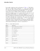
shows a block diagram of the instruction cache. The cache
holds 32 instruction-address pairs. These pairs (or cache entries) are
arranged into 16 (15-0) cache sets according to the four least significant
bits (3-0) of their address. The two entries in each set (entry 0 and entry
1) have a valid bit, indicating if the entry contains a valid instruction. The
least recently used (LRU) bit for each set indicates which entry was not
placed in the cache last (0=entry 0 and 1=entry 1).
Summary of Contents for ADSP-21261 SHARC
Page 30: ...Contents xxx ADSP 2126x SHARC Processor Hardware Reference ...
Page 40: ...Register Diagram Conventions xl ADSP 2126x SHARC Processor Hardware Reference ...
Page 58: ...Differences From Previous SHARCs 1 18 ADSP 2126x SHARC Processor Hardware Reference ...
Page 112: ...Secondary Processing Element PEy 2 54 ADSP 2126x SHARC Processor Hardware Reference ...
Page 178: ...Summary 3 66 ADSP 2126x SHARC Processor Hardware Reference ...
Page 204: ...DAG Instruction Summary 4 26 ADSP 2126x SHARC Processor Hardware Reference ...
Page 322: ...Setting Up DMA 7 32 ADSP 2126x SHARC Processor Hardware Reference ...
Page 436: ...SPORT Programming Examples 9 86 ADSP 2126x SHARC Processor Hardware Reference ...
Page 521: ...ADSP 2126x SHARC Processor Hardware Reference 11 31 Input Data Port rts IDP_ISR end ...
Page 522: ...Input Data Port Programming Example 11 32 ADSP 2126x SHARC Processor Hardware Reference ...
Page 590: ...Timer Programming Examples 14 20 ADSP 2126x SHARC Processor Hardware Reference ...
Page 796: ...I O Processor Registers A 174 ADSP 2126x SHARC Processor Hardware Reference ...
Page 800: ...B 4 ADSP 2126x SHARC Processor Core Manual ...
Page 846: ...Index I 36 ADSP 2126x SHARC Processor Hardware Reference ...


