background image

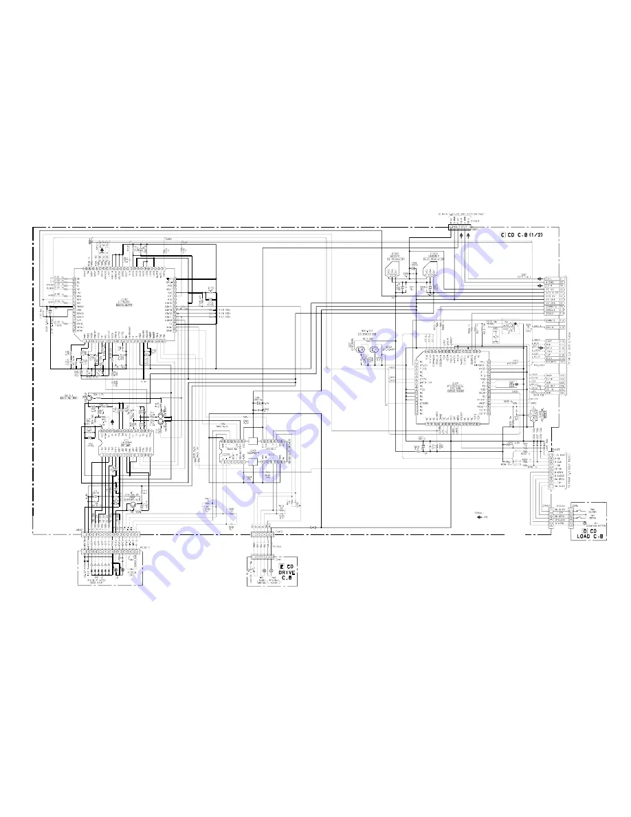
SCHEMATIC  DIAGRAM _ 4  (CD : 1 / 2 / CD  LOAD / CD  DRIVE)

– 17 –

Summary of Contents for NSX-VC8

Page 1: ...R1NM BASIC CD MECHANISM 3ZG 3 E8NM NSX VC8 HR S M Code No 09 00A 437 8R1 R E V I S I O N This Service Manual is the Revision Publishing and replaces Simple Manual NSX VC8 HR S M Code No 09 009 437 8T1 NSX VC8 SPEAKER SYSTEM CD CASSEIVER CX NVC8 REMOTE CONTROLLER RC AAS09 SX NVC8 ...

Page 2: ...UT 1 Vp p 75 ohms Cassette deck section Track format 4 tracks 2 channels stereo Frequency response 50 Hz 8000 Hz Recording system AC bias Heads Deck 1 recording playback x 1 erase x 1 Deck 2 playback x 1 Compact disc player section Laser Semiconductor laser λ 780 nm Video signal NTSC PAL color format selectable VIdeo data MPEG 1 Audio data MPEG 1 Layer 2 Speaker system SX NVC8 Speaker system 1 way...

Page 3: ...paraten används på annat sätt än vad som specificeras i denna bruksanvising kan användaren utsättas för osynling laserstrålning som överskrider gränsen för laserklass 1 PROTECTION OF EYES FROM LASER BEAM DURING SERVICING CAUTION Use of controls or adjustments or performance of proce dures other than those specified herin may result in hazardous radiation exposure ATTENTION L utillisation de comman...

Page 4: ...in power 2 2 2 2 2 Confirm that the main power is turned on and the HOLD terminal of the MICROCOMPUTER keeps the H level or not 3 3 3 3 3 When the HOLD terminal is L level the abnormality detection circuit is judged to be working correctly and the MICROCOMPUTER is judged to be good 1 Forced discharge of electrolytic capacitor of power supply block When repair is going to be attempted in the set th...

Page 5: ... ends of the electrolytic capacitor C113 that is connected to VDD of the MICROCOMPUTER with tweezers 3 3 3 3 3 Connect the AC power cord again If the MICROCOMPUTER returns to the normal operation the MICROCOMPUTER is good Note The reference number or MICROCOMPUTER pin number of transistor Q110 and electrolytic capacitor C113 can change depending on the models Be sure to check the reference numbers...

Page 6: ... 1 25F C21 87 A10 520 000 CAP E 3300 35 M SMG C22 87 016 051 000 CAP E 2200 35 M SMG C25 87 010 406 080 CAP ELECT 22 50 C26 87 010 406 080 CAP ELECT 22 50 C31 87 010 759 080 C CAP U 0 1 25F C32 87 012 286 080 CAP U 0 01 25 C34 87 010 247 080 CAP ELECT 100 50V C35 87 010 406 080 CAP ELECT 22 50 C36 87 010 112 080 CAP ELECT 100 16V C50 87 010 247 080 CAP ELECT 100 50V C51 87 010 247 080 CAP ELECT 10...

Page 7: ...05 080 CAP ELECT 10 50V C823 87 010 177 080 C CAP S 820P 50 SL C824 87 010 404 080 CAP ELECT 4 7 50V C825 87 010 596 080 CAP S 0 047 16 C836 87 012 286 080 CAP U 0 01 25 C837 87 012 286 080 CAP U 0 01 25 C842 87 012 286 080 CAP U 0 01 25 C844 87 012 286 080 CAP U 0 01 25 C850 87 010 260 080 CAP ELECT 47 25V C851 87 012 286 080 CAP U 0 01 25 C852 87 012 286 080 CAP U 0 01 25 C853 87 012 286 080 CAP...

Page 8: ...P U 100P 50CH C537 87 012 195 080 C CAP U 100P 50CH C538 87 012 195 080 C CAP U 100P 50CH C539 87 012 199 080 CAP 220P C540 87 010 759 080 C CAP U 0 1 25F C541 87 016 459 040 CAP E 470 10 SMG C543 87 010 405 040 CAP E 10 50 C590 87 010 384 040 CAP E 100 25 SME CN201 87 A60 058 010 CONN 10P V 9604S 10C CN501 87 A60 673 010 CONN 9P H 2MM JMT EMI271 87 008 372 080 FILTER EMI BL OIRNI FC201 88 910 231...

Page 9: ... CAP U 0 01 25 C603 87 010 112 080 CAP ELECT 100 16V C604 87 010 759 080 C CAP U 0 1 25F C605 87 012 286 080 CAP U 0 01 25 C606 87 012 286 080 CAP U 0 01 25 C607 87 012 178 080 C CAP U 18P 50 CH C608 87 012 178 080 C CAP U 18P 50 CH C609 87 012 274 080 CHIP CAP U 1000P 50B C610 87 012 274 080 CHIP CAP U 1000P 50B C611 87 012 274 080 CHIP CAP U 1000P 50B C612 87 012 274 080 CHIP CAP U 1000P 50B C61...

Page 10: ...TOR PART CODE 0 55 Resistor Code Dimensions mm Symbol 1 16W 1005 5 CJ 1 0 0 5 0 35 104 L t W TRANSISTOR ILLUSTRATION E C B CC5551 CSA952K KTA1266GR KTC3198GR E C B 2SC5342Y 2SC5343G 2SB1342 2SB1370 2SD1933 CSC4115BC E C B B C E E B C 2SA1162GR 2SA1235F 2SC2712GR 2SC2714O 2SC3052F 2SC5345S 0 CMBT5401 CMBT5551 DTA123JK DTA124XK DTC124XK KRA107S KRC104S RT1N441C RT1P141C 2SK360E D G S S D G 2SJ460 2S...

Page 11: ...32 31 30 29 28 27 26 25 24 23 22 21 20 19 18 17 16 15 14 13 12 11 10 9 8 7 6 5 4 3 2 1 11 A B C D E F G H I J K L M N O P Q R S T U WIRING 1 MAIN FRONT K SCAN 5 1 4 3 IMP 6 ...

Page 12: ...SCHEMATIC DIAGRAM _ 1 MAIN 1 2 AMP SECTION 12 ...

Page 13: ...SCHEMATIC DIAGRAM _ 2 MAIN 2 2 TUNER SECTION 13 ...

Page 14: ...SCHEMATIC DIAGRAM _ 3 FRONT 14 ...

Page 15: ...WIRING 2 CD 1 2 32 31 30 29 28 27 26 25 24 23 22 21 20 19 18 17 16 15 14 13 12 11 10 9 8 7 6 5 4 3 2 1 15 A B C D E F G H I J K L M N O P Q R S T U ...

Page 16: ...WIRING 2 CD 2 2 1 2 3 4 5 6 7 8 9 10 11 12 13 14 15 16 17 18 19 20 21 22 23 24 25 26 27 28 29 30 31 32 16 A B C D E F G H I J K L M N O P Q R S T U ...

Page 17: ...SCHEMATIC DIAGRAM _ 4 CD 1 2 CD LOAD CD DRIVE 17 ...

Page 18: ...SCHEMATIC DIAGRAM _ 5 CD 2 2 18 ...

Page 19: ...15 14 13 12 11 10 9 8 7 6 5 4 3 2 1 A B C D E F G H I J K L M N O P Q R S T U 19 WIRING 3 DECK ...

Page 20: ...15 14 13 12 11 10 9 8 7 6 5 4 3 2 1 A B C D E F G H I J K L M N O P Q R S T U 20 WIRING 3 CD LOAD CD DRIVE ...

Page 21: ... 21 FL HNA 10SS15T GRID ASSIGNMENT ANODE CONNECTION GRID ASSIGNMENT ANODE CONNECTION ...

Page 22: ... 22 IC BLOCK DIAGRAM ...

Page 23: ... 23 ...

Page 24: ... Power control ON OFF output 19 O C SHIFT O Clock shift output for micro computer when tuner receiving broadcast 20 O RMT O REC MUTE output 21 O BIAS O Bias ON OFF output 22 O TU ON O Tuner power supply ON OFF output 23 O CD ON O CD power supply ON OFF output 24 O CLK O PLL IC clock output 25 I TM BASE I Reference clock input for timer switch 26 O CLOSE O CD tray close data output 27 O OPEN O CD t...

Page 25: ...1 P4 O FL segment output P4 62 I TU3 P3 I O TU3 diode input FL segment output P3 63 I TU2 P2 I O TU2 diode input FL segment output P2 64 I TU1 P1 I O TU1 diode input FL segment output P1 65 NC Not connected 66 NC Not connected 67 I SD V CD I CD IC control data input 68 I O BUSY V CD O CD I O BUSY line 69 NC I Not connected 70 NC O Not connected 71 O SD V CD O CD IC control data output 72 I TUNE IF...

Page 26: ...put pin 18 ADAVDD Servo A D D A power supply pin 19 ADAVSS Servo A D D A ground pin 20 PHREF O PH reference output pin Not used 21 BHREF O BH reference output pin Not used 22 TBLO O Tracking balance output pin 23 TDO O Tracking control output pin 24 FDO O Focus control output pin 25 SPDO O Spindle control output pin 26 SLDO O Thread control output pin 27 FG I O Output driver VREF output pin FG sig...

Page 27: ... to GND 56 ASDFIN L R channel data input pin Connected to GND 57 LRSY L R clock output pin 58 DATACK O Bit clock output pin 59 DATA O L R channel data output pin 60 16M O 16 9344MHz output pin 61 SFSY O Subcode frame synchronization signal output pin This signal falls when the subcode is in the standby state 62 SBSY O Subcode clock synchronization signal output pin Not used 63 PW O Subcode P Q R S...

Page 28: ...he synchronization signal detected from the EFM signal and the internally generated synchronization signal agree 79 DFECT I O Defect pin Which becomes an input pin after reset and can be controlled externally This becomes the defect monitor pin under control by command Not used 80 EFMO O EFM signal output pin Not used ...

Page 29: ...Not connected 37 MCE ROM chip enable 38 MWE O DRAM write enable 39 VSS Ground 40 CAS O DRAM ROM interface 41 VDD3 Power supply 3 3V 42 RAS0 O DRAM ROM interface 43 RAS1 O DRAM ROM interface Not used 44 46 MA10 MA8 O DRAM ROM interface Address 47 VSS Ground 48 MA7 O DRAM ROM interface Address 49 VDD3 Power supply 3 3V 50 52 MA6 MA4 O DRAM ROM interface Address 53 VSS Ground 54 MA3 O DRAM ROM interf...

Page 30: ...0 I O Programmable I O Not used 92 PGIO8 93 VSYNC CSYNC O VSYNC CSYNC output Not used 94 AVDD PLL Analog power supply PLL 3 3V 95 NC Connected to VSS through a resistor 96 97 NC Not connected 98 AGND PLL Analog ground 99 VSS Ground 100 NC Not connected 101 HSYNC O HSYNC output Not used 102 VDD3 Power supply 3 3V 103 VCK OUT O VCK out Not used 104 VSS Ground 105 GCK I Global clock signal input 42 3...

Page 31: ...the synchronization signal detected from the EFM signal and the internally generated synchronization signal agree Not used 4 NC Not connected 5 NC Not connected 6 EMPH I Emphasis input terminal 7 DATA IN I Data input pin 8 NC Not connected 9 VSS GND 10 12 NC Connected to GND 13 EMERG I Power emergency stop L 3sec STOP 14 19 NC Not connected 20 XCDRST O CD reset output terminal 21 CMND O DATA outpu...

Page 32: ... SEL to CL680 49 NC Not connected 50 NT PAL NTSC PAL mode select 51 OSDXCS O OSD chip select 52 NC Connected to GND 53 CLVSEL I CLV mode select H CLV N Not used 54 AADSEL I Auto adjust select H Auto ON Not used 55 AVDD 5 0VDD 56 AVREF 57 HDOUT I HD OUT from CL680 58 HDIN O HD IN to CL680 59 HCK O HCK to CL680 60 OSDDATA O OSD data 61 OSDCLK O OSD clock 62 COMMAND I COMMAND from host 63 STATUS O ST...

Page 33: ...muth Adjustment DECK 1 DECK 2 Settings Test tape TTA 330 Test point TP5 Lch TP6 Rch Adjustment location Head azimuth adjustment screw Method Play back FWD the 8kHz signal of the test tape and adjust screw so that the output becomes maximum Next perform on REV PLAY mode TUNER SECTION 3 PB Frequency Response Check DECK 1 DECK 2 Settings Test tape TTA 330 Test point TP5 Lch TP6 Rch Method Play back t...

Page 34: ... 34 CD TEST MODE ...

Page 35: ... B B B B B B B B F B B B B C C B B B D B C C C C P W B P W B P W B FL ZZM 2 HT SINK TR LOW HT SINK FIN 3ZG 3 1 2 3 3 4 5 9 6 7 8 10 11 PWB HLDR WIRE 13 14 15 16 17 18 19 20 21 22 23 24 PWB HLDR FFC 26 27 12 25 a a b b CX NVC8 HRJSM File Name EXP EPS 12 9 22 ANH C 32 28 29 29 30 31 ...
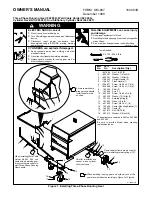
Page 36: ... REAR HRJ VCD 25 8A NHC 210 010 CABI BOTTOM VCD 26 8A NEC 201 110 HLDR PT 27 8A NEC 014 010 PANEL RIGHT 28 8A NHC 202 010 HLDR VCD 29 8A NHC 206 010 HLDR FAN 30 87 A91 751 010 FAN DSB0812M S382 400MM 31 8A NHC 201 010 COVER VCD BOTTOM 32 8A NHC 203 010 COVER VCD TOP A 87 067 822 010 BVT2 3 20 W O SLOT B 87 067 703 010 TAPPING SCREW BVT2 3 10 C 87 067 641 010 UTT2 3 8 W O SLOT BL D 87 571 092 410 T...

Page 37: ... 12 13 13 16 17 19 20 21 22 24 23 26 27 18 28 25 29 55 54 30 31 32 1 34 35 36 38 39 40 41 43 44 45 46 49 48 42 50 53 53 1 2 3 4 5 6 15 14 24 26 27 28 25 29 55 54 37 37 33 33 1 a b a b 34 61 38 39 60 40 10 7 8 9 11 12 10 43 44 45 46 47 47 51 51 56 A TERMINAL LB1 20 21 22 23 16 17 19 18 15 14 59 ...

Page 38: ... ZZM 2 28 8Z ZM1 207 010 LEVER FF 29 8Z ZM1 206 010 LEVER REW 30 8Z ZM1 210 010 LEVER REC 31 87 A90 404 010 HEAD EH LE15B 32 8Z ZM2 218 010 LEVER REC LOCK ZZM 2 33 87 A91 492 010 SW LEAF MSW18560 34 8Z ZM1 226 010 GEAR REEL L 35 8Z ZM1 241 210 SPR T PLAY 36 8Z ZM1 220 110 LEVER REC SENSOR 37 8Z ZM1 249 210 SPR T FR 38 8Z ZM1 242 310 SPR T FF REW 39 8Z ZM3 244 110 GEAR CAM TD20 40 8Z ZM1 232 010 GE...

Page 39: ... 39 CD MECHANISM EXPLODED VIEW 1 2 3ZG 3 E8NM 12 D 3 PWB MOT A b 1 2 B 8 7 11 10 4 6 5 a 9 13 14 15 C F E F a b CUSH G MAIN CUSH G MAIN 3ZG 2 E3 M1 LOADING MOTOR ...

Page 40: ...G3 204 21M 0E GEAR C 8 83 ZG3 205 019 0E GEAR D 9 83 ZG3 211 01K 0E PLATE DISC 10 83 ZG3 220 21M 0E GEAR PULLEY 2 11 83 ZG3 214 019 0E BELT L 12 83 ZG3 229 51K 1C TRAY CD 2 13 83 ZG3 210 119 1B HLDR CHUCK 14 83 ZG3 604 010 0E RING MAG 2 15 83 ZG3 212 019 0E CAP DISC A 87 067 945 119 0E VFT2 3 12 F10 B 87 251 071 410 0E U 2 6 4 C 83 ZG3 235 010 0E VFT2 2 6 8 D 87 352 075 219 0E VT2 2 6 10 E 83 ZG3 ...

Page 41: ... NO PART NO CD MECHANISM PARTS LIST 2 2 3ZG 2 E3NM A 3 6 2 5 1 PWB M21 SW1 4 1 83 ZG2 262 010 CHAS ASSY E3 2 87 A90 836 010 PICKUP KSS 213F 3 83 ZG2 235 010 GEAR A3 4 83 ZG2 236 010 GEAR MOTOR 3 5 83 ZG2 205 310 GEAR B 6 83 ZG2 253 010 SHAFT SLIDE 5 A 87 261 032 210 V 2 3 ...

Page 42: ...stall it turning to clockwise direction until click sound comes out Remove the grill frame and four pieces of rubber caps by pulling out with a flat bladed screwdriver Remove the screws from hole where installed rubber caps Insert a flat bladed screwdriver into the position indicated by the arrows and remove the panel Re move the screws of each speaker unit and then remove the speaker units TOOLS ...

Page 43: ...RD SPKR 3 8Z NSY 003 010 CORD BUSH YJSK2BL 4 8A NSM 604 010 SPKR 100 YJSL YJ3SL 4 8A NSM 606 010 SPKR 100 YJSK2BL ACCESSORIES PACKAGE LIST DESCRIPTION REF NO KANRI NO PART NO 1 8A NHC 901 010 IB H ECA M 2 8A NHC 701 010 RC UNIT RC AAS09 3 87 043 115 010 ANT FEEDER FM 4 87 006 225 010 ANT LOOP ANT NC 2 5 87 A91 017 010 PLUG CONVERSION JT 0476 ...

Page 44: ...2 11 IKENOHATA 1 CHOME TAITO KU TOKYO 110 JAPAN TEL 03 3827 3111 Printed in Singapore 2000058 0251431 ...

Reviews: