Agilent Technologies E5382A User Manual Download Page 1

A

User’s Guide

Publication number E5382-97002
December 2005

For Safety information and Regulatory information, see the pages at the back of 
this guide.

© Copyright Agilent Technologies 2002, 2005


All Rights Reserved.

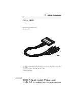
E5382A Single-ended Flying Lead


Probe Set 

(for analyzers with 90-pin pod connectors)

Summary of Contents for E5382A

Page 1: ...December 2005 For Safety information and Regulatory information see the pages at the back of this guide Copyright Agilent Technologies 2002 2005 All Rights Reserved E5382A Single ended Flying Lead Probe Set for analyzers with 90 pin pod connectors ...

Page 2: ...nded Flying Lead Probe Set Chapter 1 gives you general information such as inspection accessories supplied and characteristics of the probe Chapter 2 showsyou howtooperatetheprobeandgivesyouinformationabout some important aspects of probing and how to get the best results with your probe ...

Page 3: ...omain transmission TDT 18 Step inputs 21 Eye opening 24 5 cm Resistive Signal Lead and Solder down Ground Lead 27 Input Impedance 28 Time domain transmission TDT 30 Step input 33 Eye opening 36 Flying Lead and Ground Extender 39 Input Impedance 40 Time domain transmission TDT 41 Step input 44 Eye opening 47 Grabber Clip and Right angle Ground Lead 50 Input Impedance 51 Time domain transmission TDT...

Page 4: ...4 Contents ...

Page 5: ...1 General Information ...

Page 6: ...acquire signals from randomly located points in your target system Two E5382As are required to support all 34 channels on one 16760A Four E5382As are required to support all 68 channels of one 16753 54 55 56A or 16950A A variety of accessories are supplied with the E5382A to allow you to access signals on various types of components on your PC board Single ended flying lead probe set and an Agilen...

Page 7: ...r If the contents are incomplete or damaged notify your Agilent Technologies Sales Office Inspect the probe If there is mechanical damage or defect or if the probe does not operate properly or pass performance tests notify your Agilent Technologies Sales Office Ifthe shipping containeris damaged or the cushioning materialsshow signs of stress notify the carrier as well as your Agilent Technologies...

Page 8: ...ordering replacement parts and additional accessories Replaceable Parts and Additional Accessories Description Qty Agilent Part Number Probe Pin Kit 2 E5382 82102 High Frequency Probing Kit 4 resistive signal pins 4 solder down grounds 8 E5382 82101 Ground Extender Kit 20 16517 82105 Grabber Clip Kit 20 16517 82109 Right angle Ground Lead Kit 20 16517 82106 Cable Main 1 E5382 61601 Probe Tip to BN...

Page 9: ... for single ended clock operation is 250mV p p Input Resistance 20 kΩ Input Capacitance 1 3 pF accessory specific see accessories Maximum Recommended State Data Rate 1 5 Gb s accessory specific see accessories Minimum Data Voltage Swing 250 mV p p Minimum Diff Clock Voltage Swing 100 mV p p each side Input Dynamic Range 3 Vdc to 5 Vdc Threshold Accuracy 30 mV 2 of setting Threshold Range 3 0 V to ...

Page 10: ...Set Dimensions Operating Non operating Temperature 0 C to 55 C 40 C to 70 C Humidity up to 95 relative humidity non condensing at 40 C up to 90 relative humidity at 65 C Weight approximately 0 69 kg Dimensions Refer to the figure below Pollution degree 2 Normally only non conductive pollution occurs Occasionally however a temporary conductivity caused by condensation must be expected Indoor use ...

Page 11: ...wo E5382As are required to support all 34 channels on one 16760A Four E5382As are required to support all 68 channels of one 16753 54 55 56A or 16950A Probe set connected to the analysis module 2 Set the clock input a If you are using a differential clock select the Clock Thresh button in the analyzer setup screen of the logic analyzer Differential threshold ...

Page 12: ...he unused clock input and set the threshold to the desired level User defined threshold 3 Connect the flying leads to your target system The next section in this manual shows the recommended probe configurations in the order of best performance Select the configuration that works with your target system ...

Page 13: ...2 Operating the Probe ...

Page 14: ...r configurations have been characterized for probe loading effects probe step response and maximum usable state speed For more detailed information refer to the pages indicated for each configuration When simulating circuits that include a load model for the probe a simplified model of the probe s input impedance can usually be used The following table contains information for the simplified model...

Page 15: ...recommended state speed Details on page 130 Ω Resistive Signal Pin orange and Solder down Ground Lead 1 3 pF 1 5 Gb s page 16 5 cm Resistive Signal Lead and Solder down Ground Lead 1 6 pF 1 5 Gb s page 27 Flying Lead and Ground Extender 1 4 pF 1 5 Gb s page 39 Grabber Clip and Right angle Ground Lead 2 0 pF 600 Mb s page 50 ...

Page 16: ...rnatively forgroundyoucould use the right angle ground lead and a grabber clip as shown on page 50 Hand held probing configuration The 130 Ω resistive signal pin and solder down ground leads are identical to the accessories for the Agilent 1156A 57A 58A series oscilloscope probes They provide similar loading effects and characteristics The accessories for the 1156A 57A 58A probes are compatible wi...

Page 17: ...g schematic shows the circuit model for the input impedance of the probe when using the 130 Ω resistive signal pin orange and the solder down ground wire This model is a simplified equivalent load of the measured input impedance seen by the target Equivalent load model Measured versus modeled input impedance 2 1 8 6 104 4 2 1 8 6 4 2 1 8 6 4 2 10 1 Measured Model 104 6 8 1 2 4 6 8 1 2 4 6 8 1 Freq...

Page 18: ...n orange and solder down ground lead configuration affect the step seen by the receiver for various rise times TDT measurement schematic As the following graphs demonstrate the 130 Ω resistive signal pin and solder down ground lead configuration is the least intrusive of the four recommended configurations The graphs show that the loading effects are virtually invisible for targets with rise times...

Page 19: ...ead TDT measurement at receiver with and without probe load for 100 ps rise time TDT measurement at receiver with and without probe load for 250 ps rise time 50 mV per division 500 ps per division without probe with probe 50 mV per division 500 ps per division without probe with probe ...

Page 20: ...Lead TDT measurement at receiver with and without probe load for 500 ps rise time TDT measurement at receiver with and without probe load for 1 ns rise time 50 mV per division 500 ps per division without probe with probe 50 mV per division 500 ps per division without probe with probe ...

Page 21: ...asure Vout the signal seen by the logic analyzer The measurements were made on a mid bus connection to a 50 Ω transmission line load terminated at the receiver These measurements show the logic analyzer s response while using the 130 Ω resistive signal pin orange and solder down ground lead configuration Step input measurement schematic The following graphs demonstrate the logic analyzer s probe r...

Page 22: ...wn Ground Lead Logic analyzer s response to a 100 ps rise time Logic analyzer s response to a 250 ps rise time Note These measurements are not the true step response of the probes The true step response of a probe is the output of the probe while the input is a perfect step ...

Page 23: ...own Ground Lead Logic analyzer s response to a 500 ps rise time Logic analyzer s response to a 1 ns rise time Note These measurements are not the true step response of the probes The true step response of a probe is the output of the probe while the input is a perfect step ...

Page 24: ... PRBS These measurements show the remaining eye opening at the logic analyzer while using the 130 Ω resistive signal pin orange and solder down ground lead configuration Eye opening measurement schematic The logic analyzer Eye Scan measurement uses the same circuitry as the synchronous state mode analysis Therefore the eye openings measured are exact representations of what the logic analyzer sees...

Page 25: ... and Solder down Ground Lead Logic analyzer eye opening for a PRBS signal of 1 V p p 1000 Mb s data rate Logic analyzer eye opening for a PRBS signal of 1 V p p 1250 Mb s data rate 250 mV per division 500 ps per division 250 mV per division 500 ps per division ...

Page 26: ... and Solder down Ground Lead Logic analyzer eye opening for a PRBS signal of 1 V p p 1500 Mb s data rate Logic analyzer eye opening for a PRBS signal of 250 mV 1250 Mb s data rate 250 mV per division 500 ps per division 250 mV per division 500 ps per division ...

Page 27: ...esistor bends easily A bent resistor could affect the performance of the 5 cm resistive signal lead The 5cm resistive signal lead and the solder down ground leads are identical to theaccessoriesfortheAgilent1156A 57A 58A oscilloscopeprobes Theyprovide similar loading effects and characteristics The accessories for the 1156A 57A 58A oscilloscope probes are compatible with the E5382A probes allowing...

Page 28: ...ing schematic shows the circuit model for the input impedance of the probe when using the SMT solder down Signal red and Ground black wires This model is a simplified equivalent load of the measured input impedance seen by the target Equivalent load model Measured versus modeled input impedance 2 1 8 6 10 4 4 2 1 8 6 4 2 1 8 6 4 2 Measured Model 10 1 10 4 6 8 1 2 4 6 8 1 2 4 6 8 1 Frequency 2 4 6 ...

Page 29: ... close as possible to the point being probed Optimum Damping Resistor Value Versus Signal Lead Length If a resistor is not used the response of the probe will be very peaked at high frequencies This will cause overshoot and ringing to be introduced in the step response of waveforms with fast rise times Use of this probe without a resistor at the point being probed should be limited to measuring on...

Page 30: ...t the step seen by the receiver for various rise times TDT measurement schematic The recommended configurations are listed in order of loading on the target As the following graphs demonstrate the 5 cm resistive signal lead and solder down ground lead configuration has the 2nd best loading of the four recommended configurations The graphs show that the loading effects are virtually invisible for t...

Page 31: ...DT measurement at receiver with and without probe load for 100 ps rise time TDT measurement at receiver with and without probe load for 250 ps rise time 50 mV per division 500 ps per division without probe with probe 50 mV per division 500 ps per division without probe with probe ...

Page 32: ...TDT measurement at receiver with and without probe load for 500 ps rise time TDT measurement at receiver with and without probe load for 1 ns rise time 50 mV per division 500 ps per division without probe with probe 50 mV per division 500 ps per division without probe with probe ...

Page 33: ...sure Vout the signal seen by the logic analyzer The measurements were made on a mid bus connection to a 50 Ω transmission line load terminated at the receiver These measurements show the logic analyzer s response while using the 5 cm resistive signal lead and solder down ground lead configuration Step input measurement schematic The following graphs demonstrate the logic analyzer s probe response ...

Page 34: ...ound Lead Logic analyzer s response to a 100 ps rise time Logic analyzer s response to a 250 ps rise time Note These measurements are not the true step response of the probes The true step response of a probe is the output of the probe while the input is a perfect step ...

Page 35: ...round Lead Logic analyzer s response to a 500 ps rise time Logic analyzer s response to a 1 ns rise time Note These measurements are not the true step response of the probes The true step response of a probe is the output of the probe while the input is a perfect step ...

Page 36: ...opening at the logic analyzer while using the 5cm resistive signal lead and solder down ground lead configuration Eye opening measurement schematic The logic analyzer Eye Scan measurement uses the same circuitry as the synchronous state mode analysis Therefore the eye openings measured are exact representations of what the logic analyzer sees and operates on in state mode The following measurement...

Page 37: ... Solder down Ground Lead Logic analyzer eye opening for a PRBS signal of 1 V p p 100 Mb s data rate Logic analyzer eye opening for a PRBS signal of 1 V p p 1250 Mb s data rate 250 mV per division 500 ps per division 250 mV per division 500 ps per division ...

Page 38: ...older down Ground Lead Logic analyzer eye opening for a PRBS signal of 1 V p p 1500 Mb s data rate Logic analyzer eye opening for a PRBS signal of 250 mV p p 1250 Mb s data rate 250 mV per division 500 ps per division 250 mV per division 500 ps per division ...

Page 39: ...e soldered down wires of similar length up to 1 cm in length and expect to achieve similar results Pin probing configuration All of the measurements for the flying lead and ground extender configuration were made with standard surface mount pins on 0 1 inch centers soldered to the testfixture Theinputimpedance TDTresponse stepresponse andeyeopening measurements all include the combined load of the...

Page 40: ...llowing schematic shows the circuit model for the input impedance of the probe when using the ground extender clip This model is a simplified equivalent load of the measured input impedance seen by the target Equivalent load model Measured versus modeled input impedance 2 1 8 6 104 4 2 1 8 6 4 2 1 8 6 4 2 10 1 Measured Model 104 6 8 1 2 4 6 8 1 2 4 6 8 1 Frequency 2 4 6 8 1 2 4 6 8 1 2 4 6 109 ...

Page 41: ...he recommended configurations are listed in order of loading on the target As the following graphs demonstrate the flying lead and ground extender configuration has the 3rd best loading of the four recommended configurations However because most of the capacitance of this configuration is undamped the loading is more noticeable than the previous two configurations The graphs show that the loading ...

Page 42: ...ent at receiver with and without probe load for 100 ps rise time TDT measurement at receiver with and without probe load for 250 ps rise time 50 mV per division 500 ps per division without probe with probe 50 mV per division 500 ps per division without probe with probe ...

Page 43: ...ment at receiver with and without probe load for 500 ps rise time TDT measurement at receiver with and without probe load for 1 ns rise time 50 mV per division 500 ps per division without probe with probe 50 mV per division 500 ps per division without probe with probe ...

Page 44: ...re Vout the signal seen by the logic analyzer The measurements were made on a mid bus connection to a 50 Ω transmission line load terminated at the receiver These measurements show the logic analyzer s response while using the flying lead and ground extender configuration Step measurement schematic The following graphs demonstrate the logic analyzer s probe response to different rise times These g...

Page 45: ...ogic analyzer s response to a 100 ps rise time Logic analyzer s response to a 250 ps rise time Note These measurements are not the true step response of the probes The true step response of a probe is the output of the probe while the input is a perfect step ...

Page 46: ...Logic analyzer s response to a 500 ps rise time Logic analyzer s response to a 1 ns rise time Note These measurements are not the true step response of the probes The true step response of a probe is the output of the probe while the input is a perfect step ...

Page 47: ...how the remainingeyeopeningatthelogicanalyzerwhileusingtheflyingleadandground extender configuration Eye opening measurement schematic The logic analyzer Eye Scan measurement uses the same circuitry as the synchronous state mode analysis Therefore the eye openings measured are exact representations of what the logic analyzer sees and operates on in state mode The following measurements demonstrate...

Page 48: ...und Extender Logic analyzer eye opening for a PRBS signal of 1 V p p 1000 Mb s data rate Logic analyzer eye opening for a PRBS signal of 1 V p p 1250 Mb s data rate 250 mV per division 500 ps per division 250 mV per division 500 ps per division ...

Page 49: ...d Extender Logic analyzer eye opening for a PRBS signal of 1 V p p 1500 Mb s data rate Logic analyzer eye opening for a PRBS signal of 250 mV p p 1500 Mb s data rate 250 mV per division 500 ps per division 250 mV per division 500 ps per division ...

Page 50: ...d as a convenient method of attaching to systems with slower rise times The response of the probe is severely over peaked The load on the target is also the most severe of the 4 recommended configurations As will be demonstrated in the following sets of measurements the grabber clip and right angle ground lead configuration is only for systems with rise times slower than 1ns or effective clock rat...

Page 51: ...chematic shows the circuit model for the input impedance of the probe when using the SMD IC grabber and the right angle ground lead This model is a simplified equivalent load of the measured input impedance seen by the target Equivalent load model Measured versus modeled input impedance 2 1 8 6 10 4 4 2 1 8 6 4 2 1 8 6 4 2 10 1 Measured Model 104 6 8 1 2 4 6 8 1 2 4 6 8 1 Frequency 2 4 6 8 1 2 4 6...

Page 52: ... for various rise times TDT measurement schematic The recommended configurations are listed in order of loading on the target As the following graphs demonstrate the grabber clip and right angle ground lead configuration has the worst loading of the four recommended configurations The grabber clip is a fairly long length of undamped wire which presents a much more significant load on the target th...

Page 53: ...urement at receiver with and without probe load for 100 ps rise time TDT measurement at receiver with and without probe load for 250 ps rise time 50 mV per division 500 ps per division without probe with probe 50 mV per division 500 ps per division without probe with probe ...

Page 54: ...surement at receiver with and without probe load for 500 ps rise time TDT measurement at receiver with and without probe load for 1 ns rise time 50 mV per division 500 ps per division without probe with probe 50 mV per division 500 ps per division without probe with probe ...

Page 55: ...oad terminated at the receiver These measurements show the logic analyzer s response while using the grabber clip and right angle ground lead configuration Step measurement schematic The following graphs demonstrate the logic analyzer s probe response to different rise times These graphs are included for you to gain insight into the expected performance of the different recommended accessory confi...

Page 56: ...ad Logic analyzer s response to a 100 ps rise time Logic analyzer s response to a 250 ps rise time Note These measurements are not the true step response of the probes The true step response of a probe is the output of the probe while the input is a perfect step ...

Page 57: ...ead Logic analyzer s response to a 500 ps rise time Logic analyzer s response to a 1 ns rise time Note These measurements are not the true step response of the probes The true step response of a probe is the output of the probe while the input is a perfect step ...

Page 58: ...ent schematic The logic analyzer Eye Scan measurement uses the same circuitry as the synchronous state mode analysis Therefore the eye openings measured are exact representations of what the logic analyzer sees and operates on in state mode The following measurements demonstrate how the eye opening starts to collapseastheclockrateisincreased Thesevereovershootandringingobserved with this configura...

Page 59: ...d Logic analyzer eye opening for a PRBS signal of 1 V p p 500 Mb s data rate 1 ns rise time Logic analyzer eye opening for a PRBS signal of 1 V p p 500 Mb s data rate 500 ps rise time 250 mV per division 500 ps per division 250 mV per division 500 ps per division ...

Page 60: ...ead Logic analyzer eye opening for a PRBS signal of 1 V p p 600 Mb s data rate 1 ns rise time Logic analyzer eye opening for a PRBS signal of 250 mV 600 Mb s data rate 1 ns rise time 250 mV per division 500 ps per division 250 mV per division 500 ps per division ...

Page 61: ... is 50 Ω So the best solution for maintaining signal integrity is to terminate the line in 50 Ω after the BNC connector and a close as possible to the probe tip That technique minimizes the length of the unterminated stub past the termination The following picture shows the recommended configuration to achieve this Note This configuration has not been characterized for target loading or logic anal...

Page 62: ...ing to coaxial connectors SMA SMB SMC or other coaxial connectors BNC 50 Feedthrough Termination Adapter Ω Probe Tip E9638A Probe Tip to BNC Adapter BNC to SMA SMB SMC or other Coaxial Adapter SMA SMB SMC or other Coaxial Connector ...

Page 63: ...ounds to connect to one ground point in the system under test Using the 16515 27601 to combine grounds will have some negative impact on performance due to coupling caused by common ground return currents The exact impact depends on the signals being tested and the configuration of the test so it is impossible to predict accurately In general the faster the rise time of the signals under test the ...

Page 64: ...64 Operating the Probe Combining grounds ...

Page 65: ...11 dimensions 10 E environmental characteristics 10 eye opening 24 36 47 58 F flying lead 15 39 flying lead and grabber clip 50 flying lead and signal pin 16 G general characteristics 10 grabber clip 15 50 ground extender 15 39 lead 16 right angle 15 50 solder down 15 16 27 H hand held probing 16 I IC probing 27 input impedance 17 28 40 51 inspecting probe 7 instrument cleaning the 67 O operating ...

Page 66: ...alyzer 11 SMA SMB SMC connectors 62 solder down ground 16 27 specifications 9 state data rate 9 step input 21 33 44 55 suggested configurations 15 surface mount probing 27 T TDT 18 30 41 52 test point 16 27 threshold accuracy 9 differential 11 range 9 user defined 12 U user defined threshold 12 W weight 10 ...

Page 67: ...must be connected to the earth terminal of the power source Whenever it is likely that the ground protection is impaired you must make the instrument inopera tive and secure it against any unintended operation Service instructions are for trained service person nel To avoid dangerous electric shock do not per form any service unless qualified to do so Do not attempt internal service or adjustment ...

Page 68: ...is and is subject to being changed with out notice in future editions Further to the maximum extent per mitted by applicable law Agilent disclaims all warranties either express or implied with regard to this manual and any infor mation contained herein including but not limited to the implied warranties of merchantability and fit ness for a particular purpose Agilent shall not be liable for errors...

Reviews: