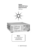
Agilent E4438C ESG Vector Signal Generator
Data Sheet
Notice
Please contact Agilent Technologies
for the latest information
or check the ESG Web site at
www.agilent.com/find/esg
Page 1: ...Agilent E4438C ESG Vector Signal Generator Data Sheet Notice Please contact Agilent Technologies for the latest information or check the ESG Web site at www agilent com find esg ...
Page 2: ...nal burst envelope 16 Composite modulation 16 Simultaneous modulation 16 Specifications for I Q Characteristics 17 I Q modulation bandwidth 17 I Q adjustments 18 Baseband generator arbitrary waveform mode 19 Baseband generator real time mode 20 Specifications for Signal Personality Characteristics 21 3GPP W CDMA 21 IS 95 CDMA 22 cdma2000 22 Enhanced multitone 23 AWGN 23 802 11 WLAN 24 Custom modul...
Page 3: ...iguration Guide for complete ordering information Literature number 5988 4085EN Specifications spec Specifications describe the instrument s warranted performance and apply after a 45 minute warm up All specifications are valid over the signal generators entire operating environmental range unless otherwise noted Supplemental character istics denoted typical or nominal provide additional nonwarran...
Page 4: ...3GPP W CDMA FDD personality cdma2000 and IS 95 A personality TDMA personality GSM EDGE GPRS EGPRS NADC PDC PHS DECT TETRA Calibrated noise AWGN personality GPS personality Signal Studio for 1xEV DO 1xEVDO Rev A Signal Studio for 1xEV DV and cdma2000 Signal Studio for 802 11 WLAN Signal Studio for Bluetooth Signal Studio for enhanced multitone Signal Studio for HSDPA over W CDMA Signal Studio for T...
Page 5: ...st Dwell time 1 ms to 60 s Number of points 2 to 65 535 Stability3 Standard With Option UNJ or 1E5 Aging rate 1 ppm yr 0 1 ppm yr or 0 0005 ppm day after 45 days Temp 0 to 55 C 1 ppm 0 05 ppm Line voltage 0 1 ppm 0 002 ppm Line voltage range 5 to 10 5 to 10 RF reference output Frequency 10 MHz Amplitude 4 dBm 2 dB RF reference input requirements Standard With Option UNJ or 1E5 Frequency 1 2 5 10 M...
Page 6: ...m 110 dBm 127 dBm 250 kHz to 2 0 GHz 0 5 0 7 0 8 1 5 2 0 to 3 GHz 0 6 0 8 1 0 2 5 3 to 4 GHz 0 8 0 9 1 3 2 5 Option 5062 4 Power level 7 to 50 to 110 to 127 dBm 50 dBm 110 dBm 127 dBm 250 kHz to 2 0 GHz 0 6 0 8 0 8 1 5 2 0 to 3 GHz 0 6 0 8 1 0 2 5 3 to 4 GHz 0 8 0 9 1 5 2 5 4 to 6 GHz 0 8 0 9 1 5 Specifications for Frequency and Power Characteristics 1 Quoted specifications for 23 C 5 C Accuracy d...
Page 7: ...t amplitude formats FSK GMSK etc Option 501 504 Option 506 0 1 dB 0 15 dB Level accuracy with ALC off1 2 0 15 dB relative to ALC on Conditions After power search is executed with burst off Level switching speed1 Option 501 504 With Option UNB Option 506 Normal operation ALC on 15 ms 21 ms 21 ms When using power search manual 83 ms 95 ms 95 ms When using power search auto 103 ms 119 ms 119 ms Speci...
Page 8: ...ator hold Off ALC Off 0 1 Elapsed time minutes Power error dB 0 5 0 45 0 4 0 35 0 3 0 25 0 2 0 15 0 10 0 05 0 2 3 5 4 6 7 1 8 9 10 Typical unit Limits Relative level accuracy Initial power 7 dBm 0 20 40 60 Final power dBm Power error dB 0 4 0 3 0 2 0 1 0 0 1 0 2 0 3 0 4 140 120 80 100 Lower limit Lower STD deviation Mean Upper STD deviation Upper limit Repeatability measures the ability of the ins...
Page 9: ... 0 25 0 3 6 4 2 0 2 4 6 8 10 Typical STD unit Lower STD deviation Upper STD deviation Lower limit Upper limit Linearity W CDMA 5750 MHz attenuator hold On ALC On 10 8 6 4 2 0 2 4 6 8 Amplitude dBm ALC Offset error dB 0 3 0 25 0 2 0 15 0 1 0 05 0 0 05 0 1 0 15 0 2 0 25 0 3 Mean Option 506 unit Lower STD deviation Upper STD deviation Lower limit Upper limit Linearity measures the accuracy of small c...
Page 10: ...itter in µUI1 7 8 Carrier SONET SDH rms jitter Standard With option UNJ frequency data rates bandwidth µUI rms µUI rms 155 MHz 155 MB s 100 Hz to 1 5 MHz 359 78 622 MHz 622 MB s 1 kHz to 5 MHz 158 46 2 488 GHz 2488 MB s 5 kHz to 15 MHz 384 74 Jitter in seconds1 7 8 Carrier SONET SDH rms jitter Standard With option UNJ frequency data rates bandwidth 155 MHz 155 MB s 100 Hz to 1 5 MHz 2 4 ps 0 6 ps ...
Page 11: ...c 1900 MHz fc 1900 MHz fc 2200 MHz fc 2200 MHz Phase noise modes 1 and 2 at fc 900 MHz fc 5 7 GHz Option 506 Specifications for Frequency and Power Characteristics I Q on CW mode CW mode CW mode PN mode 1 PN mode 2 CW mode CW mode CW mode I Q on or CW mode I Q on I Q on I Q on I Q on I Q on ...
Page 12: ...ncy accuracy relative to CW in DCFM3 5 0 1 of set deviation N x 1 Hz Distortion3 1 kHz rate dev N x 100 kHz 1 FM using external inputs 1 or 2 Sensitivity 1 Vpeak for indicated deviation Input impedance 50 Ω nominal FM path 1 and FM path 2 are summed internally for composite modulation The FM 2 path is limited to a maximum rate of 1 MHz The FM 2 path must be set to a deviation less than FM 1 path S...
Page 13: ... limited to a maximum rate of 1 MHz FM path 2 must be set to a deviation less than the FM path 1 Range 0 to 100 Resolution 0 1 Rates 3 dB bandwidth DC coupled 0 to 10 kHz AC coupled 10 Hz to 10 kHz Accuracy4 7 1 kHz rate 6 of setting 1 Distortion4 7 1 kHz rate THD Option 501 504 Option UNJ Option 506 30 AM 1 5 1 5 90 AM 4 5 AM using external inputs 1 or 2 Sensitivity 1 Vpeak to achieve indicated d...
Page 14: ... dBm standard 7 5 dBm Option UNB 4 5 dBm Option 506 1 dB Pulse modulation using external inputs Input voltage RF on 0 5 V nominal RF off 0 5 V nominal Input impedance 50 Ω nominal Internal pulse generator Square wave rate 0 1 Hz to 20 kHz Pulse Period 8 µs to 30 seconds Width 4 µs to 30 seconds Resolution 2 µs Specifications for Analog Modulation 1 Parentheses denote typical performance 2 With ALC...
Page 15: ...ms Dual sinewave mode Frequency range 0 1 Hz to 100 kHz Amplitude ratio 0 to 100 Amplitude ratio resolution 0 1 LF audio out mode Amplitude 0 to 2 5 Vpeak into 50 Ω Output impedance 50 Ω nominal Modulation types Ext 1 FM FM AM pulse and burst envelope Ext 2 FM FM AM and pulse LO HI annunciator 100 Hz to 10 MHz BW AC coupled inputs only Activated when input level error exceeds 3 nominal Internal mo...
Page 16: ...may be any two of the following Internal External 1 External 2 Multiple modulation types may be simultaneously enabled For example W CDMA AM and FM can run concurrently and all will affect the output RF This is useful for simulating signal impairments There are some exceptions FM and FM cannot be combined AM and Burst envelope cannot be combined Wideband AM and internal I Q cannot be combined Two ...
Page 17: ...ral regrowth and noise floor Typically level accuracy with ALC on will be maintained with drive levels between 0 25 and 1 0 Vrms 2 Parentheses denote typical performance dB 100 0 50 Frequency offset from carrier MHz 50 150 150 100 3 00 1 00 1 00 3 00 5 00 7 00 9 00 11 00 13 00 15 00 1800 MHz carrier 850 MHz carrier 1900 MHz carrier 2200 MHz carrier 3 00 1 00 1 00 3 00 5 00 7 00 9 00 11 00 13 00 15...
Page 18: ... Characteristics I Q adjustments Channels 2 I and Q Resolution 16 bits 1 65 536 Arbitrary waveform memory Maximum playback capacity 8 megasamples MSa channel Option 601 64 MSa channel Option 602 Maximum storage capacity 1 2 GSa Option 005 2 8 MSa Standard Waveform segments Segment length 60 samples to 8 or 64 MSa Maximum number of segments 1 024 8 MSa volatile memory 8 192 64 MSa volatile memory M...
Page 19: ...tive External delay time 10 ns to 40 sec plus latency External delay resolution 10 ns Markers Markers are defined in a segment during the waveform generation process or from the ESG front panel A marker can also be tied to the RF blanking feature of the ESG Marker polarity Negative positive Number of markers 4 Multicarrier Number of carriers Up to 100 limited by a max bandwidth of 80 MHz depending...
Page 20: ...bol rate 25 MHz Internal filters switch to 16 tap when symbol rate is between 25 and 50 MHz Symbol rate For external serial data symbol rate is adjustable from 1000 symbols sec to a maximum symbol rate of 50 Mbits sec bits symbol For internally generated data symbol rate is adjustable from 1000 symbols sec to 50 Msymbols sec and a maximum of 8 bits per symbol Modulation quality may be degraded at ...
Page 21: ...d data rate Internal burst shape control Varies with standards and bit rates Rise fall time range Up to 30 bits Rise fall delay range 0 to 63 5 bits Error vector magnitude1 1 8 GHz fc 2 2 GHz root Nyquist filters 40 MHz baseband filter EVM optimization mode 3 84 Mcps chip rate 4 dBm 7 dBm with Option UNB 1 DPCH 1 8 0 9 Level accuracy relative to CW at 800 900 1800 1900 2200 MHz 1 2 5 dBm standard ...
Page 22: ... 82 1000 2000 MHz 72 76 71 76 79 79 82 82 Rho1 4 dBm standard and Option 506 or 7 dBm Option UNB IS 95 filter 2 GHz r 0 9992 9998 Spurious emissions dBc IS 95 modified filter with equalizer and amplitude 5 dBm standard 3 dBm for Option 506 0 dBm for Option UNB Offsets from center of carrier Frequencies offsets 2 135 to 2 50 MHz 2 50 to 3 23 MHz 3 23 to 10 MHz Forward 9 channel SR3 multi carrier 1 ...
Page 23: ...0 minutes 8 tones 80 dBc suppression Temperature stability 1 dB C typical for IMD products 5 dB C worst case for LO feedthrough and unbalanced images Enhanced multitone signal with correction applied Crest factor output power set at least 16 dB below maximum power 16 dB Randomness 89 bit pseudo random generation repetition period 3 x 10⁹ years Carrier to noise ratio Magnitude error 0 2 dB at baseb...
Page 24: ... ALC On interleaver active RF blanking Off Scrambler initialization 5D Modulator atten 8 to 10 dB Support carrier setup All channels active Idle interval 100 µS 89641A settings OSR 2 Frequency 5 8 2 4 0 9 GHz Window length 8 Span 20 MHz Data type PN15 Range optimal Data length 1024 RMS video average 20 802 11a spectral mask typical performance 0 dbm at 5 805 GHz OSR 4 window length 16 1 All values...
Page 25: ...om Custom Custom Custom Custom normal up down TCH up down TCH TCH sync up control 1 2 dummyB1 2 Fcorr sync up Vox up normal traffic B dummy access down normal lowcapacity Scramble capability Yes Yes 1 This level of performance can be attained using the external I Q inputs provided the quality of the baseband signal meets or exceeds that of the ESG baseband generator 2 Parentheses denote typical pe...
Page 26: ...tatic sensitivity RBER at user specified power level measured This is the complete conformance test as defined in pri ETS 300 609 1 GSM 11 21 version 4 12 0 Dec 98 section 7 3 4 Sensitivity search Automatically finds the input level sensitivity that causes a user specified RBER normally 2 for class II bits Maximum frame count 6 000 000 speech frames GSM measurement results Class Ib bit error ratio...
Page 27: ...5 sequence data payload Uncoded PN9 PN15 Note Maximum of 4 timeslots can be turned on with EDGE EGPRS multi frame coded data Frame structure EDGE EGPRS PDCH multi frame Repeating EDGE frame Multiframe measurements1 EDGE measurement modes Static sensitivity BER BLER at user specified power level measured based on bit errors in total unencoded data and block errors in coded channels Sensitivity sear...
Page 28: ...nimum power level 136 dBm ESG minimum Maximum power level 13 dBm option dependent Power level accuracy 0 5 dB 23 5 C power and frequency dependent Relative power level 0 to 130 dB relative to timeslot under test Limited only by output power range of the ESG Timeslot under test Timeslots tested 0 to 7 A single timeslot is tested at one time No frequency hopping Encryption None Measurement triggers ...
Page 29: ...le input threshold Hi lo threshold selectable from 0 7 V TTL 1 4 V TTL 1 65 V CMOS 3 3 2 5 V CMOS 5 0 Direct measurement triggering Data and reference signal outputs Real time display Bit count Error bit count Bit error rate Pass fail indication Valid data and clock detection Automatic re synchronization Special pattern ignore Specifications for Signal Personality Characteristics Bit error rate BE...
Page 30: ...n H x 16 8 in W x 17 in D Remote programming Interface GPIB IEEE 488 2 1987 with listen and talk RS 232 LAN 10BaseT Control languages3 SCPI version 1996 0 also compatible with 8656B and 8657A B C D J1 mnemonics Functions controlled All front panel functions except power switch and knob ISO compliant The E4438C ESG is manufactured in an ISO 9001 registered facility in concurrence with Agilent Techn...
Page 31: ...externally supplying data and clock information The input signal must be synchronized with the external data input that will be output during the burst The burst power envelope and modulated data are internally delayed and re synchronized The input signal must be CMOS high for normal burst RF power or CW RF output power and CMOS low for RF off The damage levels are 0 5 to 5 5 V This female BNC con...
Page 32: ...nput is relocated to a rear panel SMB connector Data output Outputs serial data from the internal data generator or the externally supplied signal at the data input CMOS1 signal Auxiliary I O connector rear panel Event 1 output In real time mode outputs pattern or frame synchronization pulse for triggering or gating external equipment May be set to start at the beginning of a pattern frame or time...
Page 33: ... annunciator light on the display The input impedance is 50 ohms and the damage levels are 5 Vrms and 10 Vpeak If you configure your signal generator with Option 1EM this input is relocated to a female BNC connector on the rear panel GPIB Allows communication with compatible devices rear panel I input Accepts an I input either for I Q modulation or for wideband AM Nominal input impedance 50 or 600...
Page 34: ...an externally supplied symbol sync for digital modulation applications The expected input is a symbol clock signal It may be used in two modes When used as a symbol sync in conjunction with a data clock the signal must be high during the first data bit of the symbol The signal must be valid during the falling edge of the data clock signal and may be a single pulse or continuous When the symbol syn...
Page 35: ...ear panel With Option 300 321 4 MHz input Accepts a 321 4 MHz IF signal for GSM EDGE loopback testing Input amplitude range 7 dBm to 22 dBm Nominal input impedance 50 ohms SMB rear panel LAN connector LAN communication is supported by the signal generator via the LAN connector It is functionally equivalent to the GPIB connector The LAN connector enables the signal generator to be remotely programm...
Page 36: ... O connector This connector enables you to access the inputs and outputs of the baseband generator The figure below shows the Auxiliary I O pin connector configuration View looking into rear panel connector Mating connector 37 pin male D subminiature available from AMP 3M others Event 3 Event 4 Patt trig in 2 Alt pwr in Parallel data 1 GND GND GND GND GND Parallel data 8 Parallel data clk Data out...
Page 37: ...Studio for enhanced multitone Signal Studio for HSDPA over W CDMA Signal Studio for TD SCDMA Signal Studio for Noise Power Ratio NPR Signal Studio for S DMB Signal Studio for T DMB Signal Studio for pulse building Signal Studio for jitter injection Signal Studio toolkit Signal Studio for 802 16 2004 WiMAX Signal Studio for 802 16 OFDMA Signal Studio for DVB N5102A Baseband Studio digital signal in...
Page 38: ...rature number 5988 4085EN IntuiLink Software Data Sheet literature number 5980 3115EN E4438C ESG signal generation firmware personalities 3GPP W CDMA FDD Personalities Option 400 Technical Overview literature number 5988 4449EN cdma2000 and IS 95A Personalities Option 401 Technical Overview literature number 5988 4430EN GPS Personality Option 409 Technical Overview literature number 5988 6256EN TD...
Page 39: ...39 ...
Page 40: ... and gain a competitive edge by contracting with us for calibration extra cost upgrades out of warranty repairs and onsite education and training as well as design system integration project manage ment and other professional engineering services Experienced Agilent engineers and technicians world wide can help you maximize your productivity optimize the return on investment of your Agilent instru...