


USB-5820 User Manual
20
3.4
Analog Output
3.4.1
Analog Output Overview
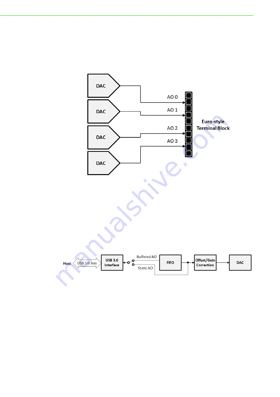
Figure 3.2 shows the functional block diagram of the USB-5820 analog output cir-
cuitry.
Figure 3.2 Analog output circuitry
The analog output (AO) signals are generated by the DACs. Each channel provides
multiple voltage and current output ranges, which can be individually configured by
software.
For buffered AO generation, blocks of digital data received from the host are first
queued in a first-in-first-out (FIFO) buffer. After offset and gain correction, the data
will be written into the DAC at a constant rate and are converted into analog wave-
forms. For static AO generation, digital data received from the host directly go
through offset and gain correction, and are written into the DAC. This is shown in Fig-
ure 3.3.
Figure 3.3 Analog output data processing
3.5
Analog Output Range
Each AO channel of the USB-5820 can generate multiple ranges of voltage or cur-
rent signal output. They can be configured by software for every channel individually.
3.5.1
Voltage Output Generation
The USB-5820 supports the following voltage output ranges: ±10 V, ±5 V, 0 ~ +10 V,
and 0 ~ +5 V. The output voltage is referenced to ground. Therefore, the load should
be connected between each AO pin and the ground pin. This is shown in Figure 3.4.
Summary of Contents for USB-5820
Page 1: ...User Manual USB 5820 4 ch 16 bit 200 kS s Isolated Analog Output USB 3 0 I O Module ...
Page 4: ...USB 5820 User Manual iv ...
Page 10: ...USB 5820 User Manual 4 Figure 1 1 Installation Flowchart ...
Page 31: ...Appendix A A Specifications ...
Page 33: ...27 USB 5820 User Manual Appendix A Specifications ...


