22
Signal Connections
Figure 3-2: Floating Source and Differential Input
AIxH
AIxL
x = 0, ..., 31
Ground Referenced Signal Source
To A/D
Converter
AIGND
+-
InstrumentationAmplifier
+
-
Input Multipexer
Page 1: ...Advance Technologies Automate the World Manual Rev 2 01 Revision Date October 4 2010 Part No 50 17032 2010 PXI 2020 2022 8 16 CH 16 Bit 250 KS s Simultaneous Sampling Card User s Manual ...
Page 2: ... or inability to use the product or documentation even if advised of the possibility of such damages This document contains proprietary information protected by copy right All rights are reserved No part of this manual may be repro duced by any mechanical electronic or other means in any form without prior written permission of the manufacturer Trademarks NuDAQ NuIPC DAQBench are registered tradem...
Page 3: ...logy China Co Ltd Address Ϟ Ꮦ ϰᮄऎᓴ 催 ᡔುऎ㢇 䏃 300 ো 201203 300 Fang Chun Rd Zhangjiang Hi Tech Park Pudong New Area Shanghai 201203 China Tel 86 21 5132 8988 Fax 86 21 5132 3588 Email market adlinktech com ADLINK Technology Beijing Address ҀᏖ ऎϞഄϰ䏃 1 োⲜ ࡼ ॺ E ᑻ 801 ᅸ 100085 Rm 801 Power Creative E No 1 B D Shang Di East Rd Beijing 100085 China Tel 86 10 5885 8666 Fax 86 10 5885 8625 Email market adl...
Page 4: ...pan Tel 81 3 4455 3722 Fax 81 3 5333 6040 Email japan adlinktech com ADLINK Technology Inc Korean Liaison Office Address 昢殾柢 昢爎割 昢爎壟 1506 25 穢壊 B D 2 猻 2F Hando B D 1506 25 Seocho Dong Seocho Gu Seoul 137 070 Korea Tel 82 2 2057 0565 Fax 82 2 2057 0563 Email korea adlinktech com ADLINK Technology Singapore Pte Ltd Address 84 Genting Lane 07 02A Cityneon Design Centre Singapore 349584 Tel 65 6844 2...
Page 5: ...ramming Library 15 2 6 PCI Configuration 16 3 Signal Connections 17 3 1 Connectors Pin Assignment 17 3 2 Analog Input Signal Connection 20 Types of Signal Sources 20 Input Connect Configurations Differential Input Mode 21 4 Function Block and Operation Theory 23 4 1 Overall Function Block Diagram 23 4 2 Basic AI Acquisition 24 Analog Input Path 24 Basic Acquisition Timing 24 AI Data Format 26 4 3 ...
Page 6: ...uts AFI 36 4 6 Trigger Modes 37 Post trigger Acquisition 37 Pre trigger Acquisition 37 Middle trigger Acquisition 38 Delay trigger Acquisition 39 4 7 Synchronizing Multiple Modules 40 SSI_TIMEBASE 41 4 8 General Purpose Timer Counter Operation 43 Timer Counter Functions Basics 43 General Purpose Timer Counter Modes 44 5 Calibration 49 5 1 Loading Calibration Constants 49 5 2 Auto calibration 50 5 ...
Page 7: ... 8 Table 2 1 SMB Connector 12 Table 2 2 TRG IO as an Input Port 12 Table 2 3 TRG IO as an Output Port 13 Table 2 4 CLK IN 13 Table 2 5 CLK OUT0 OUT1 as an Output Port 13 Table 3 1 PXI 2020 2022 68 pin VHDCI type Pin Assignment 17 Table 3 2 68 pin VHDCI type Connector Legend 18 Table 4 1 Basic Counters 25 Table 4 2 Bipolar Analog Input Range and Output Digital Code 27 Table 4 3 Summary of User cont...
Page 8: ...2022 Trigger Sources 31 Figure 4 7 External Digital Trigger Polarity and Pulse Width Re quirement 32 Figure 4 8 TRG IO Output Signal Timing 33 Figure 4 9 DAQ Signal Routing 34 Figure 4 10 Post trigger Acquisition 37 Figure 4 11 Pre trigger Mode Operation 37 Figure 4 12 Pre trigger Mode Operation 38 Figure 4 13 Middle trigger Mode Operation 38 Figure 4 14 Delay trigger Mode Operation 39 Figure 4 15...
Page 9: ...022 to fit your application needs Post trigger delay trigger pre trigger and middle trigger modes are also available to acquire data around the trigger event The PXI 2020 2022 also feature repeated trigger acquisition so you can acquire data in multiple segments with successive trigger events at extremely short rearming intervals Multiple Module Synchronization The versatile trigger options provid...
Page 10: ...ation will be stored in the on board EEPROM so that the values can be loaded and used as needed by the board 1 1 Features The PXI 2020 2022 Simultaneous Data Acquisition Card provides the following advanced features Supports 3 3V and 5V PCI signal PXI specification Rev 2 2 compliant 8 16 CH differential analog inputs Bipolar analog input Programmable gains of x1 x4 Scatter gather DMA transfer for ...
Page 11: ...7685 or equivalent Maximum sampling rate 250 kS s each channel Resolution 16 bits Input coupling DC Programmable input range 10V 2 5V Operational common mode voltage range 8V Overvoltage protection Power on Continuous 30V Power off Continuous 30V FIFO buffer size 16 K samples 8192 x 32 bits Data transfers Polling Mode Bus mastering DMA with scatter gather Input impedance 1 GΩ Trigger mode Pre Trig...
Page 12: ... voltage 0 8 V max Input high voltage 2 0 V min Output Logic Levels Output low voltage 0 4 V max Output high voltage 2 8 V min Output Driving Capacity 24 mA Maximum Input Overload 0 5 V to 5 5 V Trigger Condition Rising or Falling software selectable Minimum Pulse Width 12 5 ns Power on State Input pull low with 10KΩ resistor Data Transfer Polling mode PXI Star Trigger Receive Trigger from PXI Sta...
Page 13: ...Output Logic Levels Output low voltage 0 4 V max Output high voltage 2 8 V min Output Driving Capacity 24 mA Power on State Input pull low with 10KΩ resistor Data Transfer Polling mode Table 1 3 Digital I O General Purpose Specifications Model Name PXI 2020 2022 Number of Channels 2 up down counter timers by AFI Resolution 32 bit Compatibility Input 3 3 V or 5V TTL Output 3 3 V TTL Base clock avai...
Page 14: ...ScanIntrv 640 results in 125KS s and so on Internal Timebase Accuracy 25ppm typical External Timebase Clock Sources External from hardware IO refer to section 4 3 for details 1 PXI_10M 2 AFI 0 7 3 PXI Trigger BUS 0 4 PXI Star Trigger 5 SMB_CLK Dedicate External Clock Input From IO Connector Clock Type Digital TTL Input Frequency Range 1MHz 20MHz Input Coupling DC Input Compatibility Input 3 3V or ...
Page 15: ...ctor 68 pin VHDCI type female Operating Environment Ambient temperature 0 to 55 C Relative humidity 10 to 90 non con densing Storage Environment Ambient temperature 20 to 80 C Relative humidity 5 to 95 non condens ing Table 1 7 General Power Specifications Model Name PXI 2020 2022 3 3 V 1 5 A typical 5 V 1 3 A typical 12 V 0 35 A typical Table 1 8 Power Requirements ...
Page 16: ...ement 1 Model Number PXI 2020 2022 Function Result under 25 C 5 C Offset Error gain 1 0 6 mV Typical Gain Error gain 1 0 02 Typical 3dB small signal bandwidth gain 1 1 MHz gain 4 700 KHz System Noise gain 1 0 5 mVrms gain 4 0 2 mVrms CMRR 2 DC gain 1 80 dB gain 4 80 dB Spurious free dynamic range SFDR 87 dB Signal to noise and distortion ratio SINAD 82 dB Total harmonic distortion THD 85 dB Signal...
Page 17: ...rs preferably with magnetic heads as screws and standoffs are small and easily misplaced Recommended Installation Tools Philips cross head screwdriver Flat head screwdriver Anti static wrist strap Anti static mat The PXI 2020 2022 contains several electro static sensitive com ponents that can be easily be damaged by static electricity The equipment should be handled on a grounded anti static mat a...
Page 18: ...n Card ADLINK All in one DVD Software Installation Guide PXI 2020 2022 User s Manual Caution Do not install or apply power to equipment that is damaged or if there is missing incomplete equipment Retain the ship ping carton and packing materials for inspection Please contact your ADLINK dealer vendor immediately for assis tance Obtain authorization from your dealer before returning any product to ...
Page 19: ...gure 2 1 PXI 2020 2022 PCB Layout The ADLINK PXI 2020 2022 is packaged in a Euro card form fac tor compliant with PXI specifications measuring 160 mm in length and 100 mm in height not including connectors The connector types and functions are described as follows ...
Page 20: ...K_OUT1 is from the same source CLK OUT0 Output SMB The CLK OUTPUT 0 is a 50Ω DC coupled output CLK_OUT0 and CLK_OUT1 is from the same source CLK IN Input SMB The CLK IN is a 50Ω AC coupled external time base input Table 2 1 SMB Connector TRG IO as an Input Port Connector type SMB Compatibility 3 3 V LVTTL Low Voltage 5 V tolerant Input Logic Level Input Low voltage 0 8V max Input high voltage 2 0 ...
Page 21: ...Clock from Front Panel Connector Type SMB Clock Type Sine wave or square wave Input Impedance 50 Ω Input Coupling AC Input Range 1 VP P to 2 VP P Overvoltage Protection 2 5 VP P Table 2 4 CLK IN CLK OUT0 OUT1 as an Output Port Connector Type SMB Clock Type square wave Compatibility 3 3 V TTL Output Logic Level Output low voltage 0 2 V max Output high voltage 2 4 V min Driving Capability 24 mA Outp...
Page 22: ... s edge with the card guide in the PXI chassis 3 Slide the module into the chassis until resistance is felt from the PXI connector 4 Push the ejector upwards and fully insert the module into the chassis 5 Once inserted a click can be heard from the ejector latch 6 Tighten the screw on the front panel 7 Power on the PXI system chassis To remove the module reverse step 2 through 6 above ...
Page 23: ...tions All soft ware options are included in the ADLINK All in One DVD Programming Library For customers who are writing their own programs we provide function libraries for many different operating systems including D2K DASK Include device drivers and DLL for Windows 98 NT 2000 XP Vista 7 DLL is binary compatible across Windows 98 NT 2000 XP Vista 7 This means all applications developed with D2K D...
Page 24: ...oard basis for all PCI boards on your system Because config uration is controlled by the system and software there is no jumper setting required for base address DMA and interrupt IRQ The configuration is subject to change with every boot of the system as new boards are added or removed 3 Trouble shooting If your system doesn t boot or if you experience erratic operation with your PCI board in pla...
Page 25: ...he pin assignments of the connectors are de fined in Table 3 1 and Figure 3 2 Connector Pin Assignment Pin Pin DGND 34 68 DGND DIO1 33 67 DIO0 DIO3 32 66 DIO2 DGND 31 65 AFI0 AD TRIG Out AFI1 AD TIMER OUT 30 64 AFI2 GPTC_CLK0 DGND 29 63 AFI3 GPTC_GATE0 AFI4 GPTC_CLK1 28 62 AFI5 GPTC_GATE1 AFI6 GPTC_Out1 27 61 AFI7 GPTC_Out0 NC 26 60 NC NC 25 59 NC AIL0 24 58 AIH0 AIL8 23 57 AIH8 AGND 22 56 AGND AI...
Page 26: ...ifferential positive input for AI channel 0 15 29 31 34 68 DGND Digital ground 24 21 18 15 13 9 6 3 23 20 17 14 11 8 5 2 AIL 0 15 Input Differential negative input for AIL channels 0 15 1 4 7 10 13 16 19 22 35 38 41 44 47 50 53 56 AGND Analog ground for AI 65 AFI0 DGND In put Output Auxiliary Function Input 0 AD_TRIG_SRC0 AD TIMER_SRC0 AD_CONV_SRC0 AD TRIG Out 30 AFI1 DGND In put Output Auxiliary ...
Page 27: ...n Input 4 AD_TRIG_SRC4 AD_TIM ER_SRC4 AD_CLK_SRC4 GPTC_CLK1 62 AFI5 DGND Input Auxiliary Function Input 5 AD_TRIG_SRC5 AD_TIM ER_SRC5 AD_CONV_SR C5 GPTC_GATE1 27 AFI6 DGND In put Output Auxiliary Function Input 6 AD_TRIG_SRC6 AD_TIM ER_SRC6 AD_CLK_SRC6 GPTC_OUT1 61 AFI7 DGND In put Output Auxiliary Function Input 7 AD_TRIG_SRC7 AD_TIM ER_SRC7 AD_CLK_SRC7 GPTC_OUT0 67 33 66 32 DIO 0 3 DGND In put O...
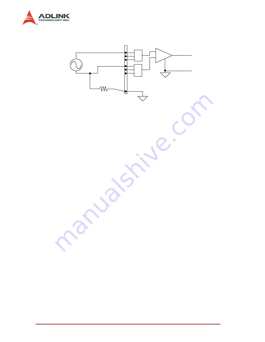
Page 28: ...l Sources A ground referenced signal means it is connected in some way to the building system That is the signal source is already con nected to a common ground point with respect to the PXI 2020 2022 assuming that the computer is plugged into the same power system Non isolated outputs of instruments and devices that plug into the buildings power system are ground referenced signal sources Floatin...
Page 29: ...g signal source to the PXI 2020 2022 card in differential input mode For floating signal sources you need to add a resistor at each channel to provide a bias return path The resistor value should be about 100 times the equivalent source impedance If the source impedance is less than 100ohms you can simply connect the negative side of the signal to AIGND as well as the negative input of the Instru ...
Page 30: ...22 Signal Connections Figure 3 2 Floating Source and Differential Input AIxH AIxL x 0 31 Ground Referenced Signal Source To A D Converter AIGND Instrumentation Amplifier Input Multipexer ...
Page 31: ...it of A D data acquisition 4 1 Overall Function Block Diagram Figure 4 1 PXI 2022 Functional Block Diagram SCSI CONNECTOR X 2 INTERFACE PXI INTERFACE AI Configure Calibration Control Analog Input Timing Control FPGA Analog Input Trigger Control Counter Timing Control PXI INTERFACE EEPROM Calibration Data Storage AI DATA SPI Control Input Gain Selection AI Calibration Select MUX CH0 16 Bit 250KS s ...
Page 32: ... Timing The trigger is a signal that starts or stops the acquisition In post trigger mode and delay trigger mode the trigger is used to initiate acquisition In pre trigger mode the trigger is used to stop acquisi tion In middle trigger mode the trigger is used to inform the acqui sition engine to acquire the specific number of data and then stop Timebase is a clock that sent to the ADC of each cha...
Page 33: ...trv 32 bit 4 to 4294967296 Scan Interval Counter This counter is a TIMEBASE 80MHz divider to the achieve equivalent sam pling rate of DAQ The equation is Sampling rate TIMEBASE ScanIntrv The value of TIMEBASE de pends on the card type Take PXI 2022 250KS s as an example the ScanIntrv 320 results in 250KS s and Sca nIntrv 640 results in 125KS s and so on DataCnt 31 bit 1 to 2147483648 Data Counter ...
Page 34: ...st decide how to trigger the A D conversion The data acquisition will start once a trigger condition is matched After the end of an A D conversion the A D data is buffered in a Data FIFO The A D data can now be transferred into the PC s memory for further process ing Two acquisition modes Software Polling and Scan acquisition are de scribed below Timing trigger modes trigger sources and transfer m...
Page 35: ...al code Full scale Range 10 V 2 5 V Least significant bit 305 2 uV 76 3 uV FSR 1LSB 9 999695 V 2 499924 V 7FFF Midscale 1LSB 305 2uV 76 3 uV 0001 Midscale 0 V 0 V 0000 Midscale 1LSB 305 2 uV 76 3 uV FFFF FSR 10 V 2 5 V 8000 Table 4 2 Bipolar Analog Input Range and Output Digital Code ...
Page 36: ...ility low jitter oscillator for the ADCs The oscillators are 80 MHz for the PXI 2020 2022 4 3 2 External Clock through Front Panel When you need a specific timebase in some applications that the onboard oscillator is not achievable a clock from an external device can replace onboard oscillator In addition external time base also provides a method to synchronize the DAQ module to other measurement ...
Page 37: ...rovide inter module synchronization and com munication Note that this function is only available when the PXI 2020 2022 is in a PXI system It s not supported when PXI 2020 2022 is in a CompactPCI system When the PXI 2020 2022 is plugged into a generic peri pheral slot in a PXI system it can receive timebase from PXI_STAR The PXI_STAR signal comes from star trigger controller is matched in propagat...
Page 38: ...6 7 232 1 Figure 4 5 Configuring Different Sampling Rate of PXI 2022 4 3 5 Timebase Exporting The PXI 2020 2022 can export timebase to one of the PXI trigger bus line 0 By software programming you can pick up a trigger line to transmit timebase clock This feature is very useful when syn chronize to multiple measurement modules TIMEBASE DATA D1 Acquisition In Progress Trigger Acquisition starts rig...
Page 39: ...status and read the A D data back when it is available This method is very suitable for applications that need to process A D data in real time Under this mode the timing of the A D con version is fully controlled under software However it is difficult to control the A D conversion rate 4 4 2 External Digital Trigger An external digital trigger occurs when a TTL rising edge or a fall ing edge is d...
Page 40: ... 4 PXI Trigger Bus The PXI 2020 2022 utilizes PXI Trigger Bus 5 as System Syn chronization In terface SSI Using the interconnected bus pro vided by PXI Trigger Bus you can easily synchronize multiple modules When configured as input the PXI 2020 2022 is served as a slave module and can accept three different SSI signals SSI_TIMEBASE PXI Trigger Bus 0 PXI Trigger Bus 5 and PXI Star Trigger Bus 1 Wh...
Page 41: ...AFI0 on front panel and PXI Trigger Bus Line 5 The TRG IO on the front panel can also be programmed to output the trigger signal when the trigger source is from software trigger Auxiliary Function Interface PXI Star Trig ger or PXI Trigger Bus Line 5 The timing characteristic is in Fig ure 4 8 Figure 4 8 TRG IO Output Signal Timing TRG IO Output Tw Tw 3 TIMEBASE Clocks ...
Page 42: ...itry s However the SSI PXI timing signals remain the same for every PXI 2020 2022 card We implemented signal multiplexers in the FPGA to individually choose the desired timing signals for the DAQ operations as shown in the Figure 4 9 Figure 4 9 DAQ Signal Routing You can utilize the flexible timing signals through our software driv ers and simply and correctly connect the signals with the PXI 2020...
Page 43: ...SSI_AD_TRIG PXI Trigger Bus 0 Refer to Section 4 5 for detailed description 3 SCAN_START the signal to start a scan which would bring the following ADCONV signals for AD conversion and could come from the internal SI_counter AFI 0 and SSI_AD_START This signal is synchronous to the TIMEBASE Note that the AFI 0 should be TTL compat ible and the minimum pulse width should be the pulse width of the TI...
Page 44: ... each rising edge of AFI 0 would bring an effec tive conversion signal Also note that the AFI 0 signal should be TTL compatible and the minimum pulse width is 20ns 4 5 2 Auxiliary Function Inputs AFI You could use the AFI in applications that take advantage of exter nal circuitry to directly control the PXI 2020 2022 series cards The AFI includes 2 categories of timing signals one group is the ded...
Page 45: ...isition starts once specified function calls are executed to begin the pre trigger operation and it stops when the trigger event occurs If the trigger event occurs after the specified amount of data has been acquired the system only stores the data before the trigger event with specified amount as illustrated in Figure 4 11 Figure 4 11 Pre trigger Mode Operation Time Operation start Trigger N samp...
Page 46: ... and after trigger event can be set individually M and N samples as illustrated in Figure 4 13 Figure 4 13 Middle trigger Mode Operation Please note that trigger event can only accepted when the speci fied amount of data has been acquired M samples If the sam pled data is not enough the trigger event will be ignored Time Operation start Acquisition start Trigger Data Trigger Event Occurs Acquisiti...
Page 47: ... in Figure 4 14 The delay time is speci fied by a 32 bit counter value so that the maximum delay time is the period of TIMEBASE X 232 1 while the minimum delay is the period of timebase Figure 4 14 Delay trigger Mode Operation Time Operation start Trigger Data Trigger Event Occurs Acquisition stop Begin to transfer data to system N samples Acquisition start Delay Time ...
Page 48: ... multiple modules synchronization The PXI 2020 2022 utilizes the PXI Trigger Bus 0 7 as the System Synchronization Interface SSI By pro viding flexible routing of timebase clock and trigger signals onto PXI Trigger Bus the PXI 2020 2022 makes the synchronization be tween multiple modules easy and simple The bi directional SSI I Os provide a flexible connection between modules which allows one SSI ...
Page 49: ...puts the onboard LVTTL time base through PXI trigger bus line 0 As an input the PXI 2020 2022 accepts the SSI_TIMEBASE signal to be the source of timebase In PXI form factor we utilize the PXI trigger bus built on the PXI backplane to provide the necessary timing signal connections All the SSI signals are routed to the J2 connector No additional cable is needed For detailed information of the PXI ...
Page 50: ...be the slaves c Set external digital trigger for Card 1 s A D operation d Set the SI_counter and the post scan counter PSC of all other cards e Start DMA operations for all cards thus all the cards are waiting for the trigger event When the digital trigger condition of Card 1 occurs Card 1 will internally generate the ADCONV signal and output this ADCONV signal to SSI_ADCONV signal of Card 2 3 and...
Page 51: ... can be controlled via hardware or software They are clock input GPTC_CLK gate input GPTC_GATE and up down control input GPTC_UPDOWN The GPTC_CLK input provides a clock source input to the timer counter Active edges on the GPTC_CLK input make the counter increment or decrement The GPTC_UPDOWN input controls whether the counter counts up or down The GPTC_GATE input is a control signal which acts as...
Page 52: ... operat ing theories under different modes are described as below Mode 1 Simple Gated Event Counting In this mode the counter counts the number of pulses on the GPTC_CLK after the software start Initial count can be loaded from software Current count value can be read back by soft ware any time without affecting the counting GPTC_GATE is used to enable disable counting When GPTC_GATE is inac tive ...
Page 53: ... initial count 0 count up mode Figure 4 17 Mode 2 Operation Mode 3 Single Pulse width Measurement In this mode the counter counts the pulse width of the signal on GPTC_GATE in terms of GPTC_CLK Initial count can be loaded from software After the software start the counter counts the number of active edges on GPTC_CLK when GPTC_GATE is in its active state After the completion of the pulse width int...
Page 54: ...f two and a pulse width of four Figure 4 19 Mode 4 Operation Mode 5 Single Triggered Pulse Generation This function generates a single pulse with programmable delay and programmable pulse width following an active GPTC_GATE edge You could specify these programmable parameters in terms of periods of the GPTC_CLK input Once the first GPTC_GATE edge triggers the single pulse GPTC_GATE takes no effect...
Page 55: ...e 6 Operation Mode 7 Single Triggered Continuous Pulse Generation This mode is similar to mode5 except that the counter gener ates conti nuous periodic pulses with programmable pulse interval and pulse width following the first active edge of GPTC_GATE Once the first GPTC_GATE edge triggers the counter GPTC_GATE takes no effect until the soft ware start is re executed Figure 4 22 illustrates the g...
Page 56: ...g the software start GPTC_GATE is used to enable disable counting When GPTC_GATE is inactive the counter halts the current count value Figure 4 23 illustrates the generation of two pulses with a pulse delay of four and a pulse width of three Figure 4 23 Mode 8 Operation 4 4 3 3 2 1 0 2 1 S o f t w a r e s t a r t 0 3 2 1 0 2 1 1 0 3 G a t e C L K C o u n t v a l u e O U T ...
Page 57: ...loading the values of TrimDACs stored in the on board EEPROM ADLINK provides software to make it easy to read the calibration constants automatically when necessary There is a dedicated space for calibration constants In the EEPROM In addition to the default bank of factory calibration con stants there are three extra user modifiable banks This means users can load the TrimDACs values either from ...
Page 58: ...s to adjust the on board calibration refer ence except when an ultra precision calibrator is available Note 1 Before auto calibration procedure starts it is recom mended to warn up the card for at least 15 minutes 2 Please remove the cable before an auto calibration pro cedure is initiated because the DA outputs would be changed in the process of calibration 5 3 Saving Calibration Constants After ...
Page 59: ...as a voltage selector switch make sure that the switch is set to the proper position for the area The voltage selector switch is set at the factory to the cor rect voltage For pluggable equipment ensure they are installed near a socket outlet that is easily accessible Secure the power cord to prevent unnecessary accidents Do not place anything over the power cord If the equipment will not be in us...
Page 60: ...lock battery CAUTION Risk of explosion if battery is replaced by an incorrect type Dispose used batteries as instructed in the instructions The equipment should be checked by service personnel if one of the following situation arises The power cord or plug is damaged Liquid has penetrated the equipment The equipment has been exposed to moisture The equipment is not functioning or does not function...