background image

miniBASE-10R 

 
Connectors, Pinouts and Jumpers 

23 

6.10. USB 

and 

LAN 

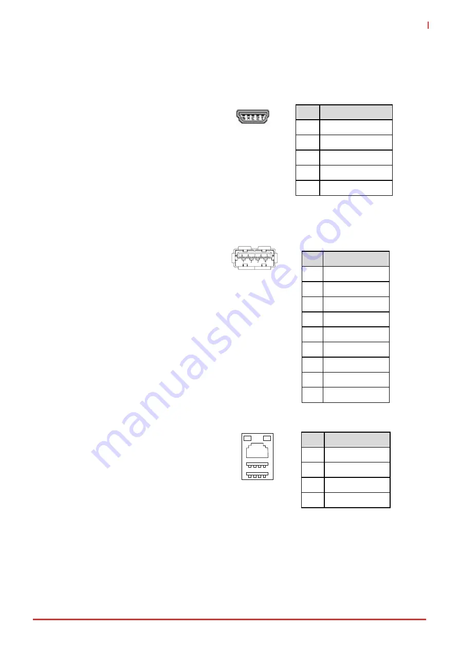
6.10.1. J10: 

Mini-USB 

Supports Mini-USB form factor 
(from USB 7 signals on AB connector) 


6.10.2.  J13: USB 3.0 x 2 

USB 2.0 compatible  
(from USB 0, USB_SS0, USB 1,  
USB_SS1 signals on AB connector) 


6.10.3.  JX14: USB 2.0 x 2 and GbE RJ-45 

USB from USB 2, USB 3, signals on AB  
Connector GbE from Intel® i210 using  
PCIe x1 signals on AB connector) 


Pin 

Signal 

1 Client_PWR_Dectect

2 USB- 

3 USB+ 

4 N.C. 

5 GND 

Pin 

Signal 

1 USB3_P5VA 

2 USB2_CMAN 

3 USB2_CMAP 

4 GND 

5 USB3A_CMRXN 

6 USB3A_CMRXP 

7 GND 

8 USB3A_CMTXN 

9 USB3A_CMTXP 

Pin 

Signal (USB) 

1 + 

5V 

2 USB- 

3 USB+ 

4 GND 

Summary of Contents for miniBASE-10R

Page 1: ...Leading EDGE COMPUTING miniBASE 10R User s Manual COM Express Type 10 Reference Carrier Board in Mini ITX Form Factor Manual Rev 1 1 Revision Date November 7 2017 Part Number 50 1V002 1010...

Page 2: ...itted to fulfill its social responsibility to global environmental preservation through compliance with the European Union s Restriction of Hazardous Substances RoHS directive and Waste Electrical and...

Page 3: ...Mechanical Drawing 9 6 Connectors Pinouts and Jumpers 11 6 1 Carrier Board Signals Type 10 11 6 2 Connector and Pinout Compatibility 12 6 3 Carrier Board Design 12 6 4 COM Express Board to Board Conne...

Page 4: ...S1 S4 33 8 2 POST 33 8 3 Indicator LEDs 34 9 Smart Battery Management System 35 9 1 Input Power 35 9 2 Charger Output Capability 35 9 3 Key Characteristics 35 9 4 Battery Settings 35 9 5 Windows OS In...

Page 5: ...10R Preface v List of Figures Figure 1 miniBASE 10R Component Locations 5 Figure 2 miniBASE 10R Functional Block Diagram 7 Figure 3 miniBASE 10R Mechanical Drawing 9 Figure 4 Carrier Board Signals Ty...

Page 6: ...vi Preface List of Tables Table 1 miniBASE 10R AB Pin Definitions 14...

Page 7: ...Ie card one Mini PCIe mSATA card slot and one SD card The miniBASE 10R integrates a Smart Battery Management System that supports two Smart Batteries and 19V adapter input The integrated Smart Battery...

Page 8: ...2 Introduction This page intentionally left blank...

Page 9: ...dary BIOS The miniBASE 10R supports the Serial Peripheral Interface SPI for COM Rev 2 1 modules Selection of active BIOS can be made by jumper settings The jumper of the secondary BIOS is JPX7 2 3 Int...

Page 10: ...4 Features This page intentionally left blank...

Page 11: ...miniBASE 10R Component Locations 5 3 Component Locations Figure 1 miniBASE 10R Component Locations See section 8 3 Indicator LEDs on page 34 for detailed LED locations...

Page 12: ...6 Component Locations This page intentionally left blank...

Page 13: ...SDIO MMC LVDS eDP 30 pin header Mini PCie PCIE0 x1 USB5 Mini PCIe SATA PCIE2 x1 RJ 45 SER0 POST 80H SDIO 8 pin header DB9 COM2 SER1 SPI Container SPI SATA1 Auto Switch SATA1 CPLD Main Input 19VDC BAT1...

Page 14: ...8 Functional Diagram This page intentionally left blank...

Page 15: ...6 99 24 29 71 29 146 39 5 08 145 09 5 08 150 17 142 07 All dimensions are shown in millimeters Tolerances should be 0 25mm unless otherwise noted The tolerances on the PCB corner locating peg holes di...

Page 16: ...10 Mechanical Drawing This page intentionally left blank...

Page 17: ...miniBASE 10R Connectors Pinouts and Jumpers 11 6 Connectors Pinouts and Jumpers 6 1 Carrier Board Signals Type 10 Figure 4 Carrier Board Signals Type 10...

Page 18: ...n The miniBASE 10R is compatible with COM Express modules in mini size form factor Type 10 pinout COM 0 Rev 2 1 6 3 Carrier Board Design The miniBASE 10R follows the PICMG COM Express Carrier Design G...

Page 19: ...A0_TX SATA1_TX 18 SUS_S4 SUS_STAT 19 SATA0_RX SATA1_RX 20 SATA0_RX SATA1_RX 21 GND FIXED GND FIXED 22 USB_SSRX0 USB_SSTX0 23 USB_SSRX0 USB_SSTX0 24 SUS_S5 PWR_OK 25 USB_SSRX1 USB_SSTX1 26 USB_SSRX1 US...

Page 20: ...PAIR4 79 LVDS_A3 LVDS_ eDP_BKLT_EN 80 GND FIXED GND FIXED 81 LVDS_A_CK eDP_TX3 DDI0_PAIR3 82 LVDS_A_CK eDP_TX3 DDI0_PAIR3 83 LVDS_I2C_CK eDP_AUX LVDS_ eDP_BKLT_CTRL 84 LVDS_I2C_DAT eDP_AUX VCC_5V_SBY...

Page 21: ...BKLT_CTRL 15 LVDS_A2 16 BKLT_EN 17 GND 18 GND 19 LVDS_A3 20 N C 21 LVDS_A3 22 LVDS_VDD_EN 23 GND 24 N C 25 LVDS_A_CLK 26 LVDS_I2C_DATA 27 LVDS_A_CLK 28 LVDS_I2C_CLK 29 GND 30 GND Pin Signal Pin Signal...

Page 22: ...Port From DDI0 signal on AB connector Connector Status 1 2 GND 2 3 5 14V Pin Signal Pin Signal 1 Lane0_P 2 GND 3 Lane0_N 4 Lane1_P 5 GND 6 Lane1_N 7 Lane2_P 8 GND 9 Lane2_N 10 Lane3_P 11 GND 12 Lane3_...

Page 23: ...evel Or PWM When set to Voltage Level the Backlight CTRL signal can be varied from 0 5V in 0 5V increments 6 6 4 JP7 Brightness PWM Source Sets the Panel Brightness PWM Source to GPU or LVDS I2C When...

Page 24: ...mpers 6 7 Audio Connectors 6 7 1 JX2 S PDIF Output Jack optical 6 7 2 JX6 S PDIF Output Header 6 7 3 JX1 Three in One Audio Phone Jack Pin Signal Pin Signal 1 SPDIF Out 2 GND Color Signal Blue Line In...

Page 25: ...r Pin Signal Pin Signal 1 WAKE 2 3 3V 3 N C 4 GND 5 N C 6 1 5V 7 CLKREQ 8 N C 9 GND 10 N C 11 REFCLK 12 N C 13 REFCLK 14 N C 15 GND 16 N C 17 N C 18 GND 19 N C 20 N C 21 GND 22 PERST 23 PERn 24 3 3V 2...

Page 26: ...Pin Signal 1 WAKE 2 3 3V 3 N C 4 GND 5 N C 6 1 5V 7 CLKREQ 8 N C 9 GND 10 N C 11 REFCLK 12 N C 13 REFCLK 14 N C 15 GND 16 N C 17 N C 18 GND 19 N C 20 N C 21 GND 22 PERST 23 PERn 24 3 3V 25 PERp 26 GN...

Page 27: ...REFCLK 12 N C 13 REFCLK 14 N C 15 GND 16 N C 17 N C 18 GND 19 N C 20 N C 21 GND 22 PERST 23 SATA_RX 24 3 3V 25 SATA_RX 26 GND 27 GND 28 1 5V 29 GND 30 SMB_CLK 31 SATA_TX 32 SMB_DATA 33 SATA_TX 34 GND...

Page 28: ...type for the J5 connector 6 9 SATA 6 9 1 J9 SATA Drive activity is indicated by LED D3 see 8 3 Indicator LEDs on page 34 6 9 2 JX9 Power for SATA Note indicates default setting Jumper Status 1 2 Mini...

Page 29: ...0 USB_SS0 USB 1 USB_SS1 signals on AB connector 6 10 3 JX14 USB 2 0 x 2 and GbE RJ 45 USB from USB 2 USB 3 signals on AB Connector GbE from Intel i210 using PCIe x1 signals on AB connector Pin Signal...

Page 30: ...1 Serial Ports J3 COM 1 J6 COM 2 Only TX RX support 6 12 I2 C SMBus and CAN Bus 6 12 1 H2 I2C Bus Pin Signal 1 BI_DA 2 BI_DA 3 BI_DB 4 BI_DB 5 BI_DC 6 BI_DC 7 BI_DD 8 BI_DD Pin Signal Pin Signal 1 N C...

Page 31: ...cts 4 pin or 3 pin type fan 6 13 2 JPX5 Fan Control Only available for 3 pin fan 6 13 3 H3 Fan Header Note indicates default setting Pin Signal 1 3 3V 2 SMB_DAT 3 SMB_CLK 4 GND Pin Signal 1 TX 2 RX 3...

Page 32: ...7 SD Card Slot From SD signal on AB connector 6 14 4 UX4 Secondary SPI BIOS Socket JPX7 BIOS Selection Pin Signal Pin Signal 1 GPI_0 2 GPO_0 3 GPI_1 4 GPO_1 5 GPI_2 6 GPO_2 7 GPI_3 8 GPO_3 Pin Signal...

Page 33: ...the power and short pins 2 and 3 6 15 2 JPX7 BIOS Selection See 7 1 SPI Secondary BIOS on page 31 for a detailed description Note indicates default setting Pin Signal 1 CPLD_TCKL 2 GND 3 CPLD_TDO 4 3...

Page 34: ...Connectors Supports dual Smart Batteries 6 16 3 JPY2 Smart Battery Configuration Select 3 cell or 2 cell battery configuration 6 16 4 JPX1 Protection Selection Note indicates default setting Pin Signa...

Page 35: ...e All ADLINK modules support S3 mode and subsequent power down of the ATX power supply For modules that connect the S3 signal PS_ON should always be set to SUS_S3 as source even when S3 mode is disabl...

Page 36: ...30 Connectors Pinouts and Jumpers This page intentionally left blank...

Page 37: ...OS and provide support for the following Testing new BIOS versions Development of firmware modifications Recovery if soldered BIOS on module is corrupted 7 1 SPI Secondary BIOS SPI is supported by PIC...

Page 38: ...32 Secondary BIOS This page intentionally left blank...

Page 39: ...Button S2 switch is the Power Button S3 switch is the Lid Button It supports Type 10 modules for ACPI power management behavior setting in OS S4 switch is the Sleep Button It supports Type 10 modules...

Page 40: ...board z D2 indicates 5VSB power for carrier board and COM Express module z D3 indicates SATA drive activity connector J9 z D4 indicates 5V power for carrier board z D5 indicates 19VDC power adapter i...

Page 41: ...lease ensure that the COM Express module supports Wide Voltage Input power 9 1 Input Power AD DC Adapter Input Battery Voltage 19V 2 cells 5 7VDC 8 4VDC 3 cells 9VDC 12 6VDC Max Current 4 7A Dependent...

Page 42: ...no device attached it will only report the presence of an AC adapter to the OS 9 5 3 Battery Present The system BIOS will report an AC adapter and two battery devices to the OS 9 5 4 Battery State Not...

Page 43: ...cautions and warnings on the equipment should be noted Please keep this equipment from humidity Do not use this equipment near water or a heat source Lay this equipment on a reliable surface when ins...

Page 44: ...200 Toll Free 1 800 966 5200 USA only Fax 1 408 360 0222 Email info adlinktech com ADLINK Technology China Co Ltd Address 300 Fang Chun Rd Zhangjiang Hi Tech Park Pudong New Area Shanghai 201203 China...

Reviews: