ADLINK Technology Inc.
LEC-
iMX6R2 User’s Guide
Page 40
copyright © 2021 ADLINK Technology Inc.
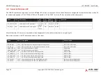
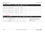
4.3.10
SPI & ESPI
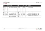
4.3.11
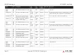
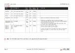
SPI0
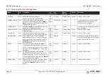
Name
Pin #
Description
I/O
Type
I/O
Level
Power
Domain
PU / PD
Comments
SPI0_CS0#
P43
SPI0 Master Chip Select 0
O
CMOS
1.8V
Standby
This signal can be used to select carrier SPI as
boot device
SPI0_CS1#
P31
SPI0 Master Chip Select 1
O
CMOS
1.8V
Standby
SPI0_CK
P44
SPI0 Clock
O
CMOS
1.8V
Standby
SPI0_DIN
P45
SPI0 Master input / Slave output
I
CMOS
1.8V
Standby
also referred to as MISO
SPI0_DO
P46
SPI0 Master output / Slave input
O
CMOS
1.8V
Standby
also referred to as MOSI
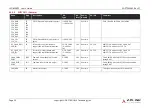
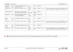
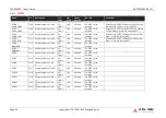
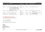
SPI1_CS0#
P54
SPI1 Master Chip Select 0
O
CMOS
1.8V
Standby
See ESPI
SPI1_CS1#
P55
SPI1 Master Chip Select 1
O
CMOS
1.8V
Standby
See ESPI
SPI1_CK
P56
SPI1 Clock
O
CMOS
1.8V
Standby
See ESPI
SPI1_DIN
P57
SPI1 Master input / Slave output
I
CMOS
1.8V
Standby
See ESPI
SPI1_DO
P58
SPI1 Master output / Slave input
O
CMOS
1.8V
Standby
See ESPI
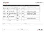
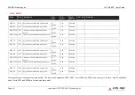
Note
: SPI0 is free to use on the carrier but support only one device through CS0
SPI1 supports a CAN bus controller on the module through CS0, that leaves CS1 free for a device on the carrier

