


MC97F6108A User’s manual
18. Reset
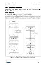
193
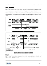
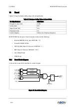
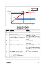
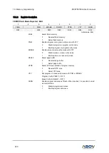
Reset Release
Config Read
POR
:VDD Input
:Internal OSC
Figure 92. Boot Process Waveform
Table 28. Boot Process Description
Process
Description
Remarks
No Operation
0.7V to 0.9V
1st POR level Detection
Internal OSC (16MHz) ON
About 1.2V to 1.6V
(INT-OSC16MHz/2)
×
29H Delay section (=5ms)
VDD input voltage must rise over than flash
operating voltage for Configure option read
Slew Rate
>=
0.025V/ms
*Ports with DSCL/DSDA are operated to
DSCL/DSDA pins with internal pull-up
resistor.
Configure option read point
About 1.5V to 1.6V
Configure Value is determined by the
writing option
Rising section to Reset Release Level
8ms point after POR or the external
Reset Release
*Ports with DSCL/DSDA are operated to
DSCL/DSDA pins with internal pull-up
resistor.
Reset Release section (BIT overflow)
I.
8ms after the external Reset Release
(External Reset)
II.
8ms point after POR (POR only)
BIT is used for Peripheral stability
Normal operation