MC96F6432
June 22, 2018 Ver. 2.9
277
VSS
R
’
R
’
R
’
R
’
VLC0
VLC1
VLC2
VLC3
VLCD
(1/ 4 BIAS)
VSS
R
’
R
’
VLC0
VLC1
VLC2
VLC3
VLCD
(1/ 2 BIAS)
VSS
R
’
R
’
R
’
VLC0
VLC1
VLC2
VLC3
VLCD
(1/ 3 BIAS)
LCTEN
DISP
C
o
n
tr
a
s
t
C
o
n
tr
o
lle
r
LCTEN
DISP
C
o
n
tr
a
s
t
C
o
n
tr
o
lle
r
LCTEN
DISP
C
o
n
tr
a
s
t
C
o
n
tr
o
lle
r
NOTES)
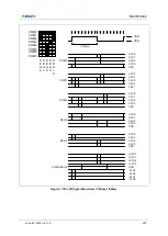
1. When the external resistor bias is selected, the internal resistors for bias are disconnected.
2. When the external resistor bias is selected, the dividing resistors should be connected like the above figure
and the needed bias pins should be selected as the LCD bias function pins (VLC0, VLC1, VLC2, and VLC3) by
P4FSR register.
- When it is 1/2 bias, the P43/VLC0 and P41/VLC2 pins should be selected as VLC0 and VLC2 functions.
The other pins can be used for normal I/O.
- When it is 1/3 bias, the P43/VLC0, P42/VLC1, and P41/VLC2 pins should be selected as VLC0, VLC1, and
VLC2 functions. Another pin can be used for normal I/O.
- When it is 1/4 bias, the P43/VLC0, P42/VLC1, P41/VLC2, and P40/VLC3 pins should be selected as VLC0,
VLC1, VLC2, and VLC3 functions
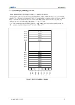
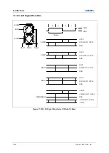
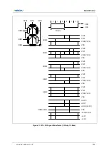
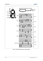
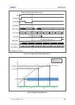
Figure 11.105 External Resistor Bias Connection
Summary of Contents for MC96F6432 Series
Page 24: ...MC96F6432 24 June 22 2018 Ver 2 9 4 Package Diagram Figure 4 1 48 Pin LQFP 0707 Package...
Page 25: ...MC96F6432 June 22 2018 Ver 2 9 25 Figure 4 2 44 Pin MQFP Package...
Page 26: ...MC96F6432 26 June 22 2018 Ver 2 9 Figure 4 3 32 Pin LQFP Package...
Page 27: ...MC96F6432 June 22 2018 Ver 2 9 27 Figure 4 4 32 Pin SOP Package...
Page 28: ...MC96F6432 28 June 22 2018 Ver 2 9 Figure 4 5 28 Pin SOP Package...


