


A96G140/A96G148/A96A148 User’s manual
15. USI
167
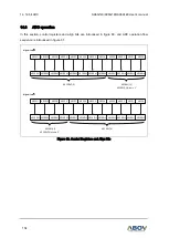
Figure 89. Asynchronous Sampling of Data and Parity Bit (USIn)
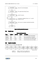
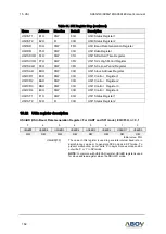
The process for detecting stop bit is same as clock and data recovery process. That is, if 2 or more
samples of 3 center values have high level, correct stop bit is detected, else a frame error (FEn) flag is
set. After deciding whether the first stop bit is valid or not, the Receiver goes to idle state and monitors
the RXDn line to check a valid high to low transition is detected (start bit detection).
Figure 90. Stop Bit Sampling and Next Start Bit Sampling (USIn)
15.10
USIn SPI mode
The USIn can be set to operate in industrial standard SPI compliant mode. The SPI mode has the
following features.
Full duplex, three-wire synchronous data transfer
Master and slave operation
Supports all four SPIn modes of operation (mode 0, 1, 2, and 3)
Selectable LSB first or MSB first data transfer
Double buffered transmit and receive
Programmable transmit bit rate
When SPI mode is enabled (USInMS[1:0]=”11”), the slave select (SSn) pin becomes active LOW input
in slave mode operation, or can be output in master mode operation if USInSSEN bit
is set to ‘0’.
RXDn
1
2
3
4
5
6
7
8
9
10 11 12 13 14 15 16
1
BIT n
1
2
3
4
5
6
7
8
1
Sample
(DBLSn = 0)
Sample
(DBLSn = 1)
RXDn
1
2
3
4
5
6
7
8
9
10 11 12 13
STOP 1
1
2
3
4
5
6
7
Sample
(DBLSn = 0)
Sample
(DBLSn = 1)
(A)
(B)
(C)