


311
Disturbance report (DRP)
&KDSWHU
0RQLWRULQJ
7DEOH 'HILQLWLRQV
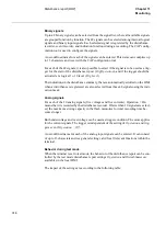
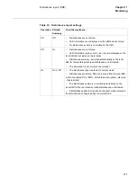
)LJXUH7KHUHFRUGLQJWLPHVGHILQLWLRQ
$QDORJVLJQDOV
Up to 10 analog signals (five voltages and five currents from the transformer module)
can be selected for recording and triggering if the disturbance recorder function is in-
stalled. If fewer than 10 signals are selected, the maximum storing capacity in the flash
memories, regarding total recording time are increased.
A user-defined name for each of the signals can be programmed in the terminal.
For each of the 10 analog signals,
2SHUDWLRQ 2Q
means that it is recorded by the dis-
turbance recorder. The trigger is independent of the setting of
2SHUDWLRQ
, and triggers
even if operation is set to
2II
. Both undervoltage and overvoltage can be used as trigger
condition. The same applies for the current signals.
1
Pre-fault or pre-trigger recording time. The time before the fault including
the operate time of the trigger. Use the setting tPre to set this time.
2
Fault time of the recording. The fault time cannot be set. It continues as
long as any valid trigger condition, binary or analog, persists (unless limited
by tLim the limit time).
3
Post fault recording time. The time the disturbance recording continues
after all activated triggers are reset. Use the setting tPost to set this time.
tLim
Limit time. The maximum allowed recording time after the disturbance
recording was triggered. The limit time is used to eliminate the conse-
quences of a trigger that does not reset within a reasonable time interval. It
limits the maximum recording time of a recording and prevents subsequent
overwriting of already stored disturbances.Use the setting tLim to set this
time.
tPre
tLim
tPost
xx00000316.vsd
1
2
3
Summary of Contents for REO 517
Page 10: ... RQWHQWV ...
Page 16: ...6 Introduction to the application manual KDSWHU QWURGXFWLRQ ...
Page 64: ...54 Blocking of signals during test KDSWHU RPPRQ IXQFWLRQV ...
Page 88: ...78 Scheme communication logic ZCOM KDSWHU LQH LPSHGDQFH ...
Page 146: ...136 Unbalance protection for capacitor banks TOCC KDSWHU XUUHQW ...
Page 166: ...156 Dead line detection DLD KDSWHU 3RZHU V VWHP VXSHUYLVLRQ ...
Page 378: ...368 Monitoring of DC analog measurements KDSWHU 0RQLWRULQJ ...
Page 384: ...374 Pulse counter logic PC KDSWHU 0HWHULQJ ...
Page 412: ...402 Serial communication modules SCM KDSWHU DWD FRPPXQLFDWLRQ ...
Page 440: ...430 LED indication module KDSWHU DUGZDUH PRGXOHV ...