72 CP9*, CR9*, CT9* Celeron M/Pentium M
Publication No. HRMCP9 Rev. B
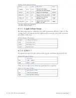
Table 8-7 Power Supply Parameters
Name
U
Imax
Description
Fuse
+12VIN
12 V
0.5 A
Supply for Hot Swap
controller and PMC-Module
U7700
a
-12VIN
-12 V
0.1 A
Supply for PMC-Module
U7700
a
USB_VCC
5 V
2 A
Supply for front panel USB
F1681
b
USBR_VCC
5 V
2 A
Supply for rear USB via
transition module
F1680
b
FUSE_VCC
5 V
2 A
Supply for front panel I/Os:
KB/MS, CRT-DCD
F9001
b
a
LTC1643L-1CGN (Linear Technologies)
b
TPS2034D (Texas Instruments)
8.11.1
Supply Voltage Range
The following ranges are defined by the CPCI specification PICMG 2.0 Rev 3.0. The
voltages have to be measured at the CR9 board (for example at the CPCI connector
pins at the solder side):
Table 8-8 Supply Voltage Range
Supply
Voltage and tolerance
+5 V
5.0 V +5 % / -3 %
+3.3 V
3.3 V +5 % / -3 %
+12 V
12.0 V +/- 5 %
8.11.2
GPIO 0..7
This general purpose I/O pins can be used as inputs, with following signal levels:
Table 8-9 GPIO Input Voltages
Signal level
low
-0.5 V ... +0.8 V
high
+2.0 V ... +5.5 V
When used as outputs, the following signal levels are supplied:
Table 8-10 GPIO Output Voltages
Signal level at current
low
-0.4 V at 6 mA sinking
high
+2.4 V at 3 mA sourcing


