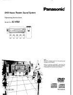
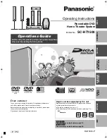
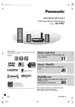
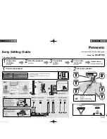
background image

SERVICE MANUAL

This manual has been provided for the use of authorized YAMAHA Retailers and their service personnel.
It has been assumed that basic service procedures inherent to the industry, and more specifically YAMAHA Products, are already
known and understood by the users, and have therefore not been restated.

WARNING:

Failure to follow appropriate service and safety procedures when servicing this product  may result in personal
injury, destruction of expensive components, and failure of the  product to perform as specified. For these reasons,
we advise all YAMAHA product owners that any service required should be performed by an authorized YAMAHA
Retailer or the appointed service representative.

IMPORTANT:

The presentation or sale of this manual to any individual or firm does not constitute authorization,  certification  or
recognition  of  any  applicable  technical  capabilities,  or establish a principle-agent relationship of any form.

The data provided is believed to be accurate and applicable to the unit(s) indicated on the cover.  The research, engineering, and service
departments of YAMAHA are continually striving  to improve YAMAHA products. Modifications are, therefore, inevitable and
specifications are subject to change without notice or obligation to retrofit. Should any discrepancy appear to exist, please contact the
distributor's Service Division.

WARNING:

Static discharges can destroy expensive components. Discharge any static electricity your body may have
accumulated by grounding yourself to the ground buss in the unit (heavy gauge black wires connect to this buss).

IMPORTANT:

Turn the unit OFF during disassembly and part replacement. Recheck all work before you apply power to the unit.

IMPORTANT NOTICE

1 0 1 0 8 3

SERVICE MANUAL

SELF-DIAGNOSIS FUNCTION /

自己診断機能

......................................................... 23–30

AMP ADJUSTMENT ................................................... 31
IC DATA ................................................................ 32–40
BLOCK DIAGRAMS ............................................. 41–43
PIN CONNECTION DIAGRAM ................................... 44
PRINTED CIRCUIT BOARDS .............................. 45–58
SCHEMATIC DIAGRAMS .................................... 59–74
REPLACEMENT PARTS LIST ............................. 75–85
REMOTE CONTROL .................................................. 86

■ 

CONTENTS

TO SERVICE PERSONNEL ..................................... 2–3
PREVENTION OF ELECTROSTATIC DISCHARGE ...... 4
LOCALE MANAGEMENT INFORMATION ................. 4

SYSTEM COMPOSITION / 

システム構成 ....................

5

FRONT PANELS ....................................................... 5–6
REAR PANELS ....................................................... 7–10
REMOTE CONTROL PANEL ..................................... 11

SPECIFICATIONS / 

参考仕様

.............................. 12–14

INTERNAL VIEW ........................................................ 15

DISASSEMBLY PROCEDURES / 

分解手順

........ 16–20

PROTECTION INFORMATION DISPLAY /

プロテクション情報の表示

.................................... 21–22

• The DVX-1000 consists of the DVR-1000, NX-SW1000 and NX-P1000.
• When accepting a repair order from the user, it is recommended to receive DVR-1000, NX-SW1000

and NX-P1000 as a set for the repair work.

DVX-1000は、DVR-1000、NX-SW1000  および  NX-P1000  で構成されています。

修理依頼を受ける際、DVR-1000、NX-SW1000 および NX-P1000 を一緒にお預かりすることを推奨します。

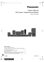
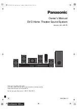
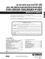
DVD RECEIVER/SUBWOOFER/SPEAKERS

DVR-1000/NX-SW1000/NX-P1000

DVD HOME THEATER SOUND SYSTEM 

DVX-1000

DVX-1000

© 2008 YAMAHA CORPORATION. All rights reserved.

This manual is copyrighted by YAMAHA and may not be copied or

redistributed either in print or electronically without permission.


  ’08.03

Summary of Contents for DVX-1000

Page 1: ...r to exist please contact the distributor s Service Division WARNING Static discharges can destroy expensive components Discharge any static electricity your body may have accumulated by grounding you...

Page 2: ...herein may result in hazardous radiation exposure WARNING CHEMICAL CONTENT NOTICE The solder used in the production of this product contains LEAD In addition other electrical electronic and or plastic...

Page 3: ...increase the laser emission level from the device Laser Diode Properties Type Semiconductor laser GaAlAs Wave length 650 nm DVD 784 nm VCD CD Output Power 7 mW DVD VCD CD Beam divergence 60 degree WA...

Page 4: ...in the DVD mechanism may be damaged due to static electricity from clothes or the human body Use caution to prevent electrostatic damage when servicing or handling the DVD mechanism 1 Grounding for el...

Page 5: ...FRONT PANELS STANDBY ON EJECT DIMMER BASS TREBLE ENTER DIRECT DVD CD TUNER SURROUND AUX SUBTITLE ANGLE ZOOM AUDIO MUTE AREA MODE USB ENHANCER NIGHT REPEAT ON SCREEN MENU SET UP TOP MENU RETURN FREQ TE...

Page 6: ...6 DVX 1000 DVX 1000 Front view Side view Front view Side view NX SW1000 NX P1000...

Page 7: ...7 DVX 1000 DPX 1200 DVX 1000 REAR PANELS R K A L models G model DVR 1000 Rear view Bottom view Rear view Bottom view...

Page 8: ...8 DVX 1000 DVX 1000 F model J model Rear view Bottom view Rear view Bottom view DVR 1000...

Page 9: ...9 DVX 1000 DPX 1200 DVX 1000 R model A model K model G F models NX SW1000...

Page 10: ...10 DVX 1000 DVX 1000 L model J model Red Black NX SW1000 NX P1000 Rear view Bottom view...

Page 11: ...PEAT ON SCREEN MENU SET UP TOP MENU RETURN PRESET PRESET PROG A B SHUFFLE SLEEP DVX 1000 WM23860 STANDBY ON EJECT DIMMER BASS TREBLE ENTER DIRECT DVD CD TUNER SURROUND AUX SUBTITLE ANGLE ZOOM AUDIO MU...

Page 12: ...76 0 to 90 0 MHz AM Tuning Range AM K A G F J models 531 to 1602 kHz R L models 531 to 1602 kHz 530 to 1700 kHz DISC SECTION Laser Type Semiconductor Disc Diameter 12cm Video Decoding MPEG 1 MPEG 2 Di...

Page 13: ...e 16cm Frequency Response 35Hz 100Hz 10dB Input Sensitivity AUX In 300 mV Dimensions W x H x D 230 x 477 x 440 mm 9 1 16 x 18 3 4 x 17 5 16 Weight 16 0 kg 35 lbs 4 oz Finish Black color Accessories Sy...

Page 14: ...ced Yamaha Active Servo Technology which Yamaha has developed for reproducing higher quality super bass sound DIMENSIONS Unit mm inch 78 3 1 16 38 1 1 2 435 17 1 8 208 8 3 16 477 18 3 4 230 9 1 16 440...

Page 15: ...SB P C B u MONO P C B i AV P C B o POWER SUPPLY UNIT 0 HDMI P C B 1 LOADER ASS Y 2 FRONT 3 P C B DVR 1000 NX SW1000 q DRIVER WOOFER w MAIN 1 P C B e DSP 1 P C B r DSP 3 P C B t DSP 2 P C B y POWER TRA...

Page 16: ...2 c Remove 1209 1303 and CN3 Fig 2 d Remove the top cabinet Fig 2 2 Removal of Loader Ass y a Remove screw e and screw r Fig 3 b Remove 1100 and 1103 Fig 3 c Remove the USB P C B Fig 3 d Remove 2 scr...

Page 17: ...xible flat cable Unlocked Locked Loader ass y ASSY r e u y t MONO P C B Support MPEG MPEG USB P C B 1101 1102 1110 1104 1105 1100 1103 1304 1301 1301 Fig 3 Fig 4 a ASSY b Fig 4 How to manually eject a...

Page 18: ...he metalblade on the like to prevent possible deformation of the front panel sub ass y When installing the front panel sub ass y apply quick drying bond or the like to dowels and then fit them into do...

Page 19: ...Remove 6 screws w Fig 7 d Pull out the rear panel ass y slowly Fig 7 e Remove CB15 Fig 7 f Remove the rear panel ass y Fig 7 When Checking the P C B Connect all the removed connectors during disassem...

Page 20: ...f the front panel ass y forward gradually and remove it from 4 dowels Fig 3 At this time use care not to cause damage to the hook in the upper part of the front panel ass y When installing the front p...

Page 21: ...tion Normal no protection function I protection PS1 protection 1 PS2 protection 2 PS3 protection 3 THM protection AMP DC protection DC Displayed Flashing Off D300 D301 D302 D303 NX SW1000 Connect the...

Page 22: ...ly section is abnormal Detection port PRV3 DSP P C B 93 pin of microprocessor IC13 Detected at AC1 D24 of MAIN P C B 5V IC12 of MAIN P C B 4 THM protection Cause Abnormal temperature of heat sink Dete...

Page 23: ...R Vol 0 dB 2 MUTE CHECK 1 MUTE OFF Vol 20 dB 2 SPEAKERS MUTE 3 FRONT L R MUTE 4 SUBWOOFER MUTE 3 RESERVED Not applied to this model 4 OUTPUT PORT CHECK 1 Not applied to this model 2 Not applied to thi...

Page 24: ...000 to AC outlets Next turn on the power by pressing the STANDBY ON key of DVR 1000 or STANDBY ON key of the remote controller while pressing the key for service SW300 on the rear panel of NX SW1000 A...

Page 25: ...ENU key on the remote controller Sub menu selection To select the sub menu press the applicable numeric key among 1 to 4 on the remote controller Numeric 1 key Select the sub menu No 1 Numeric 2 key S...

Page 26: ...Input level AUX IN Both ch 20 dBm SPEAKER OUTPUT 1 kHz FRONT L R SUBWOOFER 50Hz 21 5 dBm Input level AUX IN Both ch 20 dBm SPEAKER OUTPUT 1 kHz FRONT L R 16 0 dBm SUBWOOFER 50Hz 0 5 dBm Input level A...

Page 27: ...trol On Off 4 LIM Limiter level control High Low 80 SWRY Subwoofer output relay control On Off 52 RYC Power relay control On Off 53 PB INT Interruput for I2C communication request High Low 29 Y CLK DV...

Page 28: ...a test tone is output in the following order more than a speaker 5 3 SUBWOOFER OUTPUT 5 4 FRONT L R 1kHz SUBWOOFER 100Hz FRONT L R 1kHz SUBWOOFER 100Hz 6 RESERVED 5 3 SUBWOOFER OUTPUT A test tone is...

Page 29: ...5 3rd digit The indicator for service indicates the firmware version of the microprocessor in the binary system This indication is available only while the numeric key of each sub menu on the remote...

Page 30: ...this model 12 RESERVED Not applied to this model 13 DSP PROGRAM WRITING Used when writing the DSP firmware 13 1 READY FOR WRITING Used to set to the mode ready for writing the DSP firmware 13 2 Not a...

Page 31: ...r is turned on confirm that the voltage across the terminals of R79 FRONT L ch R80 FRONT R ch R71 SUBWOOFER ch are between 0 1 mV and 10 0 mV R79 FRONT L ch R80 FRONT R ch R71 SUBWOOFER ch 0 1 mV 10 0...

Page 32: ...O GND POWER I O I I O GND POWER I O DSP_MUTE3 P12V DGND P33V P33V P33V DGND P12V P12V DGND DSP_BCK P12V DGND DSP_WCK P33V DGND P12V DGND DSP_CEN3 DSP_SDO3 DSP_SCK3 DGND P12V DSP_SDI3 DGND P12V P33V D...

Page 33: ...utside pull up 1 2V power supply 3 3V power supply Ground 1 2V power supply 3 3V power supply Ground Ground 1 2V power supply 1 2V power supply Ground 1 2V power supply Ground 3 3V power supply Outsid...

Page 34: ...ED7 ED8 P12V DGND P33V ED4 ED5 ED3 ED2 ED1 ED0 P12V DGND DSP_BUSYN3 P33V DIR_WCK DIR_BCK P33V DGND DIR_SDO DSP_SW DSP_S DSP_C DGND P12V DSP_F DIR_SDO DSP_BCK DGND DSP_WCK DSP_RDYN3 P12V DGND DIR_MCK P...

Page 35: ...TCK DGND P12V P12V TRSTN DGND P12V P33V DGND XMCK P33V P33V DGND P12V 3 3V power supply Ground DSP interrupt signal output General purpose I O port no used General purpose I O port no used General pu...

Page 36: ...1 RX2 RX3 DGND DVDD RX4 RX5 VI RX6 UI DVDD DGND 37 38 39 40 41 42 43 44 45 46 47 48 24 23 22 21 20 19 18 17 16 15 14 13 SDIN SLRCK SBCK RDATA RLRCK DVDD DGND RBCK RMCK AGND AVDD LPF DO DI CE CL XMODE...

Page 37: ...Analog power supply for PLL 3 3 V Analog GND for PLL R system clock output pin 256 fs 512 fs XIN VCO R bit clock input output pin 64 fs Digital GND Digital power supply 3 3 V R LR clock input output p...

Page 38: ...GND CGND CGND CGND CGND CGND CGND CGND CGND CGND CGND AMP_PRSTN MODE_SW POWER_RY DAC_SMUTE Output timer A 5 Input timer B 6 Internal peripheral functions Watchdog timer 15 bit DMAC 2 channel D A conve...

Page 39: ...e 23 P7_7 TA3IN P7_7 O CODEC Reset 24 P7_6 TA3OUT P7_6 O DIR Reset 25 P7_5 TA2IN W P7_5 O D60Y Reset 26 P7_4 TA2OUT W P7_4 I D60Y Ready 27 P7_3 CTS2 RTS2 TA1IN V P7_3 O EEPROM Chip Enable reserve 28 P...

Page 40: ...ric Current Observation 74 P1_6 D14 INT4 P1_6 I Self mode SW 75 P1_5 D13 INT3 INT3 I RC Signal Detection 76 P1_4 D12 P1_4 FMT O Front Speaker Mute Control 77 P1_3 D11 P1_3 SWMT O Sub Woofer Mute Contr...

Page 41: ...YUV 0 8 GND 9 YUV 1 10 GND 11 YUV 2 12 GND 13 YUV 3 14 5V 15 YUV 4 16 3V3 17 YUV 5 18 3V3 19 YUV 6 20 GND 21 YUV 7 22 GND 23 MCLK 24 GND 25 VSYN 26 GND 27 SPDIF_OUT 28 GND 29 HDMI_DET 30 HSYN 1 GND 2...

Page 42: ...2 3 4 5 6 7 1204 1 2 3 4 5 6 7 8 9 10 11 1115 1 2 3 4 5 6 7 8 9 10 11 12 13 1108 1 2 3 4 5 6 7 8 9 10 1107 1 2 3 4 5 6 7 8 9 10 11 12 13 14 15 16 17 18 19 20 21 1209 1 2 3 4 5 6 7 8 9 10 11 12 13 14 1...

Page 43: ...5 1 1 2 3 5 7 16 14 11 JK200 To DVR 1000 IC4 DIR 6 SPDIF 3 IC1 DSP 21 DIRSD0 143 IC10 CODEC 6 DSP SW 12 27 FL 21 FR SW 28 150 DSP F 145 IC13 MICROPROCESSOR IC14 IC15 2 6 2 1 7 1 IC5 SDRAM IC7 FLASH I...

Page 44: ...VQ LC89057W VF4D E YAC523 VZ S29AL004D70TFI020 W9816G6CH 7 M30626FHPFP D60YA003BPYP225 14 7 1 8 20 10 1 11 24 13 12 1 25 36 37 48 22 12 11 1 23 33 34 44 48 24 1 25 51 50 31 81 80 100 30 1 50 25 1 26 2...

Page 45: ...pe 1xxx Connector 3xxx Resistor 5xxx Coil 7xxx IC Transistor FET 2xxx Capacitor 4xxx SMD jumper 6xxx Diode 9xxx Wire jumper USB Top view USB Bottom view AV 1107 USB Cable Ass y PRINTED CIRCUIT BOARDS...

Page 46: ...Ass y Loader Ass y HDMI 1000 AV 1205 AV 1203 The first digit of a component indicates the component type 1xxx Connector 3xxx Resistor 5xxx Coil 7xxx IC Transistor FET 2xxx Capacitor 4xxx SMD jumper 6x...

Page 47: ...00 The first digit of a component indicates the component type 1xxx Connector 3xxx Resistor 5xxx Coil 7xxx IC Transistor FET 2xxx Capacitor 4xxx SMD jumper 6xxx Diode 9xxx Wire jumper MONO Bottom view...

Page 48: ...4xxx SMD jumper 6xxx Diode 9xxx Wire jumper AV Top view HDMI 1402 Power Supply Unit CN1 FRONT 3 1301 MONO 1302 MONO 1104 MONO 1105 FRONT 1 1100 USB 1103 AM FM Tuner HDMI 1302 HDMI 1401 HDMI 1301 SYSTE...

Page 49: ...000 The first digit of a component indicates the component type 1xxx Connector 3xxx Resistor 5xxx Coil 7xxx IC Transistor FET 2xxx Capacitor 4xxx SMD jumper 6xxx Diode 9xxx Wire jumper AV Bottom view...

Page 50: ...xxx Connector 3xxx Resistor 5xxx Coil 7xxx IC Transistor FET 2xxx Capacitor 4xxx SMD jumper 6xxx Diode 9xxx Wire jumper FRONT 2 1201 Power Supply Unit CN3 FRONT 1 Top view FRONT 1 Bottom view FRONT 2...

Page 51: ...istor 5xxx Coil 7xxx IC Transistor FET 2xxx Capacitor 4xxx SMD jumper 6xxx Diode 9xxx Wire jumper FRONT 1 1104 FRONT 5 1500 FRONT 3 1303 FRONT 4 1400 FRONT 2 1202 FRONT 2 Top view FRONT 4 Top view FRO...

Page 52: ...a component indicates the component type 1xxx Connector 3xxx Resistor 5xxx Coil 7xxx IC Transistor FET 2xxx Capacitor 4xxx SMD jumper 6xxx Diode 9xxx Wire jumper HDMI Top view AV 1112 MONO 1304 AV 120...

Page 53: ...00 The first digit of a component indicates the component type 1xxx Connector 3xxx Resistor 5xxx Coil 7xxx IC Transistor FET 2xxx Capacitor 4xxx SMD jumper 6xxx Diode 9xxx Wire jumper HDMI Bottom view...

Page 54: ...NC 5V REM LED0 LED1 LED2 LED3 SELF_SW DGND TVccd TCK RES DGND TMODE TRXD BOOT TTXD 5VI2C SCL_1 DG SDA_1 G_SPD SPDIF GND_RY 12RY PB_DET MUTE PB_INT S5V 5 5 5C MG MG MG PRV1 PRV2 PRV3 THM PDET RESET 12...

Page 55: ...1 2 3 4 5 6 7 8 A B C D E F 55 DVX 1000 DSP 1 Side B Ref No Location D1 B5 D2 B5 D3 E5 D4 B5 D5 B5 D6 D5 D7 D5 D9 E3 D10 D3 D11 D3 D12 D3 D18 B5 Semiconductor Location...

Page 56: ...e A DSP 3 Side A GND_RY 12RY PB_DET MUTE PB_INT SYSTEM CONNECTOR DSP 1 W2 DSP 1 W7 DSP 1 W8 5VI2C SCL_1 DG SDA_1 G_SPD SPDIF TVccd TCK RES DGND TMODE TRXD BOOT TTXD DSP 1 W3 5V REM LED0 LED1 LED2 LED3...

Page 57: ...FMT 1 19 SP SP 1 4 8 5 1 4 8 5 5 8 4 1 5 8 4 1 MAIN 1 Side A MAIN 1 Side B NX SW1000 Ref No Location D1 B6 D2 B6 D3 B2 D4 B2 D5 D2 D6 B2 D7 B2 D8 E4 D9 E4 D10 B5 D11 B2 D12 B2 D13 C2 D14 C5 D15 B5 D16...

Page 58: ...RV1 PRV2 PRV3 THM PDET RESET 12 AGND 12 S12 RYC AC2 E AC2 NC AC3 AC3 S5V 5 5 5C MG MG MG ACIN L ACIN N N L MAIN 2 Side A MAIN 2 Side B NX SW1000 MAIN 3 Side A POWER TRANSFORMER MAIN 2 CB16 AC IN VOLTA...

Page 59: ...3183 150R 2195 47u 16V 330K 3174 3168 10K 1u0 2159 1u8 5136 F156 2134 100n 2139 100n BLM18P 5122 60R 15K 3144 F125 56K 3163 5130 27M BSH103 7108 T129 3107 100R T127 2121 100n 2142 100n 100n 2118 2243...

Page 60: ...3 2 1 48 17 16 9 M29W160ET70N6F 7303 2Mx8 1Mx16 FLASH 25 24 T229 22R 3361 3392 1 22R T275 T273 3328 22R 10K 3375 22R 3398 22R 3407 T215 22R 3348 T205 T216 5 4 74HC1G125 7306 2 3 1 T240 3315 22R T218...

Page 61: ...4 2 3 10 20 7 15 DRIVER 8 12 18 2 T336 FOR DVD MM1623XFBE 7103 2130 100n 2185 22u 3207 6 3V 1K0 1K2 3134 1K5 3147 BC857B 7108 4K7 3202 GND 7126 2 5 3 4 8 9 PUMH7 10 11 12 13 2 3 4 5 6 7 1115 HLW13S 2...

Page 62: ...300 33R 2346 330u 10V 3350 T218 100n 2305 1K0 3419 4K7 3418 2376 1u0 2338 10u 5VA GND GND GND T222 3314 33R 5V 600R 5301 T582 T584 7319 BC847B 3375 10K 3 4 5 6 7 8 9 14 15 16 1 10 11 12 13 2 LAC1315 0...

Page 63: ...8 6108 1N4148 3128 4K7 330R 3131 3130 330R 2128 22n 27R 3106 10K 3107 2134 10n I123 I115 I113 7106 BC847B 2120 100p 10K 3147 3102 27R 100p 2127 1 2 3 4 5 6 7 319804003070 1104 3119 100R 100R 3118 1 3...

Page 64: ...1205 SKRP 1210 GND_K I208 I202 BZX384 C6V8 6202 KEY2 KEY1 LED_BLUE STANDBY_KEY EJECT_KEY 5VSTBY KEY2 STANDBY_KEY 5VSTBY EJECT_KEY 5VSTBY KEY1 LED_BLUE to FRONT 1 _1104 to FRONT 5 _1500 to FRONT 4 _14...

Page 65: ..._OUT_7 1 HSYNC1_PORT1 5 HSYNC2_PORT1 208 HSYNC_PORT2 4 IN_CLK1_PORT1 10 IN_CLK2_PORT1 41 IN_SEL 156 OE 157 PLL_PVDD 158 PLL_PVSS 47 RESET_N 21 R Cr CbCr_0 22 R Cr CbCr_1 23 R Cr CbCr_2 25 FIELD_ID_POR...

Page 66: ...A0 2 A1 3 A2 13 INT_ 5 4 5VD 7201 PCF8574T 2 3 1 74LVC1G125GW 7207 BSN20 7203 F237 F233 3228 3293 10K 1R0 47R 3240 22R 3298 22R 3296 3297 22R PCM_MCLK_IN 3295 22R 47R 3248 10n 2218 3272 4K7 AV BC847B...

Page 67: ...P2 4 5 6 7 8 9 10 11 1003 3 E11 1301 D14 1302 H14 1303 G10 1305 D14 1310 B2 2300 B9 2302 C7 6 3318 F 2A 1206 0R 5305 2304 B4 2305 B4 2306 D9 2349 2341 JAPAN VER 11 12 13 14 A B C D 2 P2 AZ3 F G H I A...

Page 68: ...3411 2423 100n 3495 22R 2430 22u 6 3V 10K 3 5 1 2 3482 74HCT1G66GW 7409 4 1K8 3443 4417 1 2 10K 3463 2 BSN20 7420 4415 1 2428 10p 3418 390R 3424 47R 47R 3438 BSN20 7419 22K 3483 3402 300R 100n 2444 2...

Page 69: ...LK DREQ1 TIOC3D 195 PD12 D28 PINT4 SD_D0 DACK1 TIOC4A 194 PD13 D29 PINT5 SD_D1 TEND1 TIOC4B 238 PC13 RD WR 75 PC14 WAIT 20 PC1 A1 15 PC2 CS2 14 PC3 CS3 13 PC4 WE0 DQMLL 10 PC5 WE1 DQMLU WR 8 PC6 WE2 D...

Page 70: ...pecial characteristics are marked Z and must be replaced with parts having specifications equal to those originally installed Schematic diagram is subject to change without notice POWER SUPPLY UNIT to...

Page 71: ...GNAL GENERATOR CELL ARRAY BANK 0 R O W D E C O D E R COLUMN DECODER SENSE AMPLIFIER CELL ARRAY BANK 1 R O W D E C O D E R COLUMN DECODER SENSE AMPLIFIER NX SW1000 IC13 M30626FHPFP Single chip 16 bit C...

Page 72: ...0 0 0 0 0 0 IC17 YAC523 VZ Digital volume 3 IN1 34 OUT1 OUT2 VolB 50kohm VolA 30kohm 45 TE1 44 TE2 39 ZCEN2 38 ZCEN1 2 AVDD 46 DGND 47 REF 1 AVSS 43 SDATAO OD 41 SDATAI 42 SCLK 40 20 19 18 CSN Contro...

Page 73: ...H2 Page 74 A5 Page 74 A6 0 1 11 6 12 0 0 1 0 1 0 1 0 0 0 0 0 0 0 0 0 0 0 0 0 0 0 0 0 0 0 0 0 0 17 1 46 5 47 7 47 5 47 7 47 7 0 47 7 47 5 0 0 0 1 0 47 5 0 1 0 0 0 0 0 0 47 5 0 0 47 5 47 5 47 5 47 5 47...

Page 74: ...ER DOWN DETECT IC14 IC12 IC10 IC11 FRONT L s 9 R157 RD35715 15K VU99960 MA8270 H D31 s 10 s 9 s 10 1P 0 22 to DSP 1 _W5 to DSP 1 _W6 to MAIN 1 _W2A to MAIN 1 _W3A to MAIN 1 _W1A to MAIN 2 _CB16 SPEAKE...

Page 75: ...CORE FET CHP CHIP FET FL DSPLY FLUORESCENT DISPLAY FLTR CE CERAMIC FILTER FLTR COMB COMB FILTER MODULE FLTR LC RF LC FILTER EMI GND MTL GROUND PLATE GND TERM GROUND TERMINAL HOLDER FUS FUSE HOLDER IC...

Page 76: ...49 US061100 C CE CHP 10pF 50V B 01 C50 UR838100 C EL 100uF 16V 01 C51 UA654680 C MYLAR 0 068uF 50V J 02 C52 UA653100 C MYLAR 1000pF 50V J 03 C53 US135100 C CE CHP 0 1uF 16V 01 C54 UR837100 C EL 10uF 1...

Page 77: ...CHP 0 1uF 16V B 01 C154 US062100 C CE CHP 100pF 50V B 01 C155 156 US035100 C CE CHP 0 1uF 16V B 01 C157 US062100 C CE CHP 100pF 50V B 01 C159 160 US035100 C CE CHP 0 1uF 16V B 01 C161 US062100 C CE C...

Page 78: ...9A00 IC KIA78L05BP 02 IC17 X4325A00 IC YAC523 EVR2 06 Q1 VV556400 TR 2SC2412K Q R S 01 Q2 WC435000 TR DGT KRC102S RTK 01 Q3 V4096100 TR 2SC4614 S T 02 Q4 V4096000 TR 2SA1770 S T 03 Q5 VV655000 TR DGT...

Page 79: ...0 C MYLAR 470pF 50V J 01 C36 WJ605000 C MYLAR 0 01uF 50V J 01 C37 WJ603300 C MYLAR 470pF 50V J 01 C38 VR169200 C MYLAR 0 47uF 50V 01 C39 WJ602900 C MYLAR 100pF 50V K 01 C40 UR867330 C EL 33uF 50V 01 C...

Page 80: ...VD631600 DIODE 1SS133 176 01 D20 21 VT332900 DIODE 1SS355 01 Z D23 WA653100 DIODE BRG KBP103G 1A 200V 02 Z D24 WA653200 DIODE BRG TS6P03G 6A 200V 04 D25 26 WC398800 DIODE KDS160 RTK 01 Z D27 WJ286700...

Page 81: ...35 4270 HF45 4330 HJ35 4470 HF45 4470 HF45 4560 HF45 4680 HF45 4750 HF45 4820 HF45 4910 HF45 5100 HJ35 5110 HF45 5120 HF45 5150 HJ35 5160 HF45 5180 HF45 5200 HF45 5220 HF45 5270 HF45 5330 HF45 5390 HF...

Page 82: ...250 250 250 251 290 152 251 250 150 295 251 251 250 251 250 250 250 250 250 1001 1001 1001 8013 1001 5 2 1 4 121 124 124 252 252 250 251 250 250 250 251 251 163 251 1001 3 1006 8002 8002 8012 1004 100...

Page 83: ...CABLE ASS Y 2P 140mm 3139 241 03551 JGF Z 8002 AAX80010 CABLE ASS Y 2P 140mm 3139 241 03121 RKAL 8005 AAX89320 FLEXIBLE FLAT CABLE 16P 180mm P 1mm 3139 111 02361 8007 AAX89370 FLEXIBLE FLAT CABLE 21P...

Page 84: ...8 WM140100 COVER DSP 2 31 WF765200 PW HEAD S TIGHT SCREW 4x8 10 MFZN2B3 01 2 32 WE774400 BIND HEAD B TIGHT SCREW 3x8 MFZN2B3 01 2 33 WE774600 SCREW IC 3x18 MFZN2W3 01 2 34 WF002600 PW HEAD B TIGHT SCR...

Page 85: ...89050 SPEAKER TERMINAL ASS Y BLACK 430485 5 AAX89120 FRONT PANEL ASS Y with GRILLE EMBLEM 470430 6 AAX89000 COVER TOP ASS Y with TW CABLE 470431 7 AAX89010 COVER BOTTOM ASS Y 470432 18 AAX89140 DAMPIN...

Page 86: ...0 78 0F 78 00 7C 85 K47 7C 83 7C A1 7C B9 7C 82 7C BA 78 21 78 50 78 1E 78 22 78 CB 78 1F 78 C6 78 4A 78 9C 78 DE 78 4B 78 BC 78 21 78 50 78 1E 78 22 78 CB 78 1F 78 C6 78 4A 78 9C 78 DE 78 4B 78 BC 78...

Reviews: