


DRX-1
DRX-1
1
SERVICE MANUAL
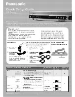
DVD RECORDER
DRX-1
1 0 0 8 2 1
■
CONTENTS
TO SERVICE PERSONNEL ...................................... 2~3
PREVENTION OF ELECTRO STATIC DISCHARGE ............. 4
LOCALE MANAGEMENT INFORMATION ................... 4
FRONT PANELS ............................................................ 5
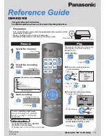
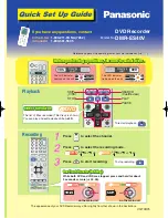
REMOTE CONTROL ...................................................... 5
REAR PANELS .............................................................. 6
SPECIFICATIONS ...................................................... 6~8
DISASSEMBLY PROCEDURES ................................... 9
SERVICE POSITION .............................................. 10~11
DIAGNOSTIC SOFTWARE ................................... 12~41
FAULTFINDING TREES ........................................ 42~68
ALIGNMENTS ........................................................ 69~71
CIRCUIT DESCRIPTIONS ..................................... 72~90
ABBREVIATION LIST ........................................... 91~96
IC DATA ............................................................... 97~105
BLOCK DIAGRAM ............................................. 107~108
WIRING DIAGRAM .................................................... 109
PRINTED CIRCUIT BOARD .............................. 110~143
SCHEMATIC DIAGRAM .................................... 144~186
EXPLODED VIEW .............................................. 187~188
MECHANICAL PARTS LIST ..................................... 189
EXPLODED VIEW (FRONT ASS'Y) .......................... 190
MECHANICAL PARTS LIST (FRONT ASS'Y) ......... 191
MECHANICAL PARTS LIST (ACCESSORIES) ....... 191
IMPORTANT NOTICE
This manual has been provided for the use of authorized YAMAHA Retailers and their service personnel.
It has been assumed that basic service procedures inherent to the industry, and more specifically YAMAHA Products, are already
known and understood by the users, and have therefore not been restated.
WARNING:
Failure to follow appropriate service and safety procedures when servicing this product may result in personal
injury, destruction of expensive components, and failure of the product to perform as specified. For these reasons,
we advise all YAMAHA product owners that any service required should be performed by an authorized
YAMAHA Retailer or the appointed service representative.
IMPORTANT:
The presentation or sale of this manual to any individual or firm does not constitute authorization, certification or
recognition of any applicable technical capabilities, or establish a principle-agent relationship of any form.
The data provided is believed to be accurate and applicable to the unit(s) indicated on the cover. The research, engineering, and
service departments of YAMAHA are continually striving to improve YAMAHA products. Modifications are, therefore, inevitable
and specifications are subject to change without notice or obligation to retrofit. Should any discrepancy appear to exist, please
contact the distributor's Service Division.
WARNING:
Static discharges can destroy expensive components. Discharge any static electricity your body may have
accumulated by grounding yourself to the ground buss in the unit (heavy gauge black wires connect to this buss).
IMPORTANT:
Turn the unit OFF during disassembly and part replacement. Recheck all work before you apply power to the unit.
P.O.Box 1, Hamamatsu, Japan
Summary of Contents for DRX-1
Page 99: ...DRX 1 DRX 1 99 TMP93C071 IC7803 ...
Page 100: ...DRX 1 DRX 1 100 STV5348 IC7990 UDA1334TS IC7506 ...
Page 106: ...DRX 1 DRX 1 106 MEMO ...
Page 133: ...A B C D E F G H I J 1 2 3 4 5 6 7 DRX 1 133 PRINTED CIRCUIT BOARD DVIO P C B Part 1 Top View ...
Page 134: ...2 A B C D E F G H I J 1 3 4 5 7 DRX 1 6 134 PRINTED CIRCUIT BOARD DVIO P C B Part 2 Top View ...
Page 192: ...DRX 1 192 DRX 1 ...