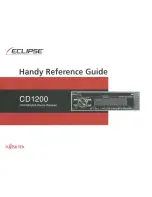
CRX-330/
NS-BP1
1
0/NS-BP1
0
0
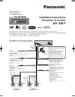
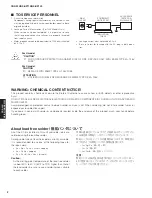
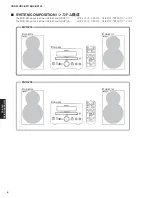
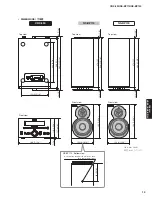
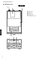
The MCR-330 consists of the CRX-330 and NS-BP110.
The MCR-230 consists of the CRX-330 and NS-BP100.
MCR-330 は、CRX-330、NS-BP110 で構成されています。
MCR-230 は、CRX-330、NS-BP100 で構成されています。
1 0 1 1 2 6
SERVICE MANUAL
IMPORTANT NOTICE
This manual has been provided for the use of authorized YAMAHA Retailers and their service personnel.
It has been assumed that basic service procedures inherent to the industry, and more specifi cally YAMAHA Products, are already known
and understood by the users, and have therefore not been restated.
WARNING:
Failure to follow appropriate service and safety procedures when servicing this product may result in personal injury,
destruction of expensive components, and failure of the product to perform as specifi ed. For these reasons, we advise
all YAMAHA product owners that any service required should be performed by an authorized YAMAHA Retailer or
the appointed service representative.
IMPORTANT:
The presentation or sale of this manual to any individual or fi rm does not constitute authorization, certifi cation or
recognition of any applicable technical capabilities, or establish a principle-agent relationship of any form.
The data provided is believed to be accurate and applicable to the unit(s) indicated on the cover. The research, engineering, and service
departments of YAMAHA are continually striving to improve YAMAHA products. Modifications are, therefore, inevitable and
specifi cations are subject to change without notice or obligation to retrofi t. Should any discrepancy appear to exist, please contact the
distributor's Service Division.
WARNING:
Static discharges can destroy expensive components. Discharge any static electricity your body may have
accumulated by grounding yourself to the ground buss in the unit (heavy gauge black wires connect to this buss).
IMPORTANT:
Turn the unit OFF during disassembly and part replacement. Recheck all work before you apply power to the unit.
■
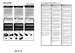
CONTENTS
TO SERVICE PERSONNEL ........................................ 2–4
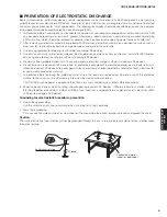
PREVENTION OF ELECTROSTATIC DISCHARGE ...... 5
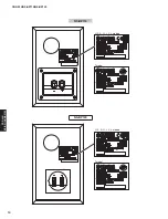
SYSTEM COMPOSITION /
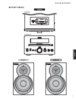
FRONT PANELS ............................................................. 7
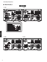
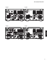
REAR PANELS ......................................................... 8–10
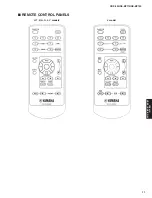
REMOTE CONTROL PANELS ..................................... 11
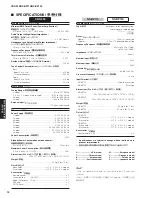
SPECIFICATIONS /
................................. 12–13
INTERNAL VIEW .......................................................... 14
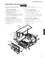
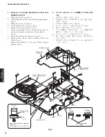
DISASSEMBLY PROCEDURES /
..................................... 18–23
....................................... 24–38
DISPLAY DATA ............................................................. 39
IC DATA ................................................................... 40–46
PIN CONNECTION DIAGRAMS ............................. 47–48
BLOCK DIAGRAM ........................................................ 49
PRINTED CIRCUIT BOARDS ................................. 50–55
SCHEMATIC DIAGRAMS ....................................... 57–61
REPLACEMENT PARTS LIST ................................ 63–79
REMOTE CONTROL ..................................................... 80
animate '08.12
P.O.Box 1, Hamamatsu, Japan
Copyright © 2008
All rights reserved.
This manual is copyrighted by YAMAHA and may not be copied or
redistributed either in print or electronically without permission.
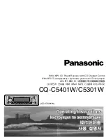
CD RECEIVER /
SPEAKERS
CRX-330/
NS-BP110/NS-BP100
For U, T, K, A, G, L, V and J models
This service manual is for the CRX-330/NS-BP110/NS-BP100 (U, T, K, A, G, L, V and J models).
For service manual of the CRX-330/NS-BP110 (B model), please refer to the following publication number:
CRX-330/NS-BP110 (B model):
101137
MICRO COMPONENT SYSTEM
MCR-330/MCR-230