background image

•  When accepting a repair order from the user, it is recommended to receive BD-940 and R-840 as a set for the repair 

work.

•  The MCR-940 consists of the R-840, BD-940 and NS-BP300.

This service manual is for the BD-940. For service manual of the R-840/NS-BP300, please refer to the following 
publication number:

R-840/NS-BP300:

1011 5 3

•  When BD module P.C.B. of this unit is replaced, the serial number and new MAC address MUST be reported to Yamaha 

Corporation  by e-mail.

E-mail: [email protected]

For more information, refer to “SERVICE PRECAUTIONS”.

BD-940

Copyright © 2009 

 All rights reserved.

This manual is copyrighted by YAMAHA and may not be copied or

redistributed either in print or electronically without permission.

1 0 1 1 5 4

SERVICE MANUAL

IMPORTANT NOTICE

This manual has been provided for the use of authorized YAMAHA Retailers and their service personnel.

It has been assumed that basic service procedures inherent to the industry, and more specifi cally YAMAHA Products, are already known 

and understood by the users, and have therefore not been restated.

WARNING:


Failure to follow appropriate service and safety procedures when servicing this product may result in personal injury, 
destruction of expensive components, and failure of the product to perform as specifi ed.  For these reasons, we advise 

all YAMAHA product owners that any service required should be performed by an authorized YAMAHA Retailer or 

the appointed service representative.

IMPORTANT:

 The presentation or sale of this manual to any individual or fi rm does not constitute authorization, certifi cation  or 

recognition of any applicable technical capabilities, or establish a principle-agent relationship of any form.

The data provided is believed to be accurate and applicable to the unit(s) indicated on the cover.  The research, engineering, and service 

departments of YAMAHA are continually striving to improve YAMAHA products.  Modifications are, therefore, inevitable and 

specifi cations are subject to change without notice or obligation to retrofi t.  Should any discrepancy appear to exist, please contact the 

distributor's Service Division.

WARNING:


Static discharges can destroy expensive components.  Discharge any static electricity your body may have 
accumulated by grounding yourself to the ground buss in the unit (heavy gauge black wires connect to this buss).

IMPORTANT:

 Turn the unit OFF during disassembly and part replacement.  Recheck all work before you apply power to the unit.

 CONTENTS

TO SERVICE PERSONNEL  ........................................ 2–3
PREVENTION OF ELECTROSTATIC DISCHARGE  
...... 4
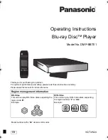
REGION MANAGEMENT INFORMATION  
..................... 5
SYSTEM COMPOSITION  
................................................ 6
FRONT PANEL  
............................................................... 7
REAR PANELS  
............................................................... 8
REMOTE CONTROL PANEL  
.......................................... 9
SPECIFICATIONS  
................................................... 10–12
INTERNAL VIEW 
 .......................................................... 13
SERVICE PRECAUTIONS  
...................................... 14–17

DISASSEMBLY PROCEDURES  ............................. 18–21
UPDATING FIRMWARE  
.......................................... 22–26
SELF-DIAGNOSTIC FUNCTION  
............................ 27–31
DISPLAY DATA  
............................................................. 32
IC DATA  
................................................................... 33–35
PIN CONNECTION DIAGRAMS  
............................. 36–37
BLOCK DIAGRAM  
........................................................ 39
PRINTED CIRCUIT BOARDS  
................................. 40–44
SCHEMATIC DIAGRAMS  
....................................... 45–48
REPLACEMENT PARTS LIST  
................................ 49–53
REMOTE CONTROL  
..................................................... 54
SYSTEM CONNECTOR  
.......................................... 55–56
SETTINGS  
............................................................... 57–59

'09.11

P.O.Box 1, Hamamatsu, Japan

BLU-RAY DISC PLAYER

BD-940

MICRO COMPONENT SYSTEM

MCR-940

Summary of Contents for BD-940

Page 1: ...entative IMPORTANT The presentation or sale of this manual to any individual or firm does not constitute authorization certification or recognition of any applicable technical capabilities or establish a principle agent relationship of any form The data provided is believed to be accurate and applicable to the unit s indicated on the cover The research engineering and service departments of YAMAHA...

Page 2: ... to test for leakage with the AC plug in both polarities WALL OUTLET EQUIPMENT UNDER TEST AC LEAKAGE TESTER OR EQUIVALENT INSULATING TABLE WARNING CHEMICAL CONTENT NOTICE About lead free solder WARNING Laser Safety This product contains a laser beam component This component may emit invisible as well as visible radiation which may cause eye damage To protect your eyes and skin from laser radiation...

Page 3: ...layer is switched off This primary area is not shielded so it is possible to accidentally touch copper tracks and or components when servicing the player Service personnel have to take precautions to prevent touching this area or components in this area Note The screws on the BD DVD mechanism may never be touched removed or re adjusted Handle the BD DVD mechanism with care when the unit has to be ...

Page 4: ...se can generate electrical charges sufficient to damage ES devices 6 Do not remove a replacement ES device from its protective package until immediately before you are ready to install it Most replacement ES devices are packaged with leads electrically shorted together by conductive foam aluminum foil or comparable conductive material 7 Immediately before removing the protective material from the ...

Page 5: ... and other limited viewing uses only unless otherwise authorized by Macrovision Corporation Reverse engineering or disassembly is prohibited REGION MANAGEMENT INFORMATION This BD DVD player is designed and manufactured to respond to the Region Management Information that is recorded on a BD DVD disc If the Region code number described on the BD DVD disc does not correspond to the Region code numbe...

Page 6: ... receive the R 840 and BD 940 as a set for the repair work The MCR 940 consists of the R 840 BD 940 and NS BP300 This service manual is for the BD 940 For service manual of the R 840 NS BP300 please refer to the following publication number R 840 NS BP300 101153 NS BP300 NS BP300 BD 940 R 840 MCR 940 ...

Page 7: ...7 BD 940 BD 940 FRONT PANEL B G F models Front view Top view ...

Page 8: ...8 BD 940 BD 940 REAR PANELS B G models F model ...

Page 9: ...9 BD 940 BD 940 REMOTE CONTROL PANEL B G F models Key colors A Red B Green C Yellow D Blue ...

Page 10: ...cable 0 6 m x 1 for MCR 940 R 840 NS BP300 Indoor FM antenna x 1 DAB wire antenna B model x 1 DOCK cover x 1 Speaker cable 2 0 m x 2 Specifications are subject to change without notice due to product improvements iPod is a trademark of Apple Inc registered in the U S and other countries Made for iPod means that an electronic accessory has been designed to connect specifically to iPod and has been ...

Page 11: ...d or was obtained from a video provider licensed to provide AVC VC 1 Video No license is granted or shall be implied for any other use Additional information may be obtained from MPEG LA LLC HDMI the HDMI logo and High Definition Multimedia Interface are trademarks or registered trademarks of HDMI Licensing LLC AVCHD and the AVCHD logo are trademarks of Panasonic Corporation and Sony Corporation B...

Page 12: ...nd Digital Output Bitstream PCM Dynamic Range Control Normal Shift Auto Quick Start Yes No Auto Power Off Yes No HDMI Control Yes No Playback Setting Parental Control Yes No DVD Level 8 and Off Level 1 7 BD No Limit 0 99 year s Disc Language Disc Priority Language Select the language for subtitles audio and menus displayed on the screen Angle Mark Display Yes No PIN Code Setting Yes Sets the passw...

Page 13: ...13 BD 940 BD 940 INTERNAL VIEW Top view Front view Rear view BD MODULE P C B MAIN 4 P C B POWER P C B MAIN 2 P C B BD MECHANISM UNIT MAIN 1 P C B MAIN 3 P C B 1 2 3 4 5 6 7 4 7 1 2 3 5 6 ...

Page 14: ...Fig 1 E mail ycav keycontrol gmx yamaha com Check the Serial Number The serial number SER No xxxxxxx can be found at the rear panel of this unit Fig 2 Fig 1 Fig 2 Rear view Serial number xxxxxxxxx Send this e mail to Yamaha Corporation ycav keycontrol gmx yamaha com ycav keycontrol gmx yamaha com BD 940 xxxxxxxxx Model name Serial number New MAC address ...

Page 15: ... this unit in the standby mode press the On Standby key of this unit to turn on the power 2 Set this unit to the Communication Setup mode by procedure below Press the SETUP key Select the Setting menu Select the Communication Setup menu Fig 3 System control cable This unit BD 940 TV monitor R 840 Video pin cable Audio Video Settings Quick Start Auto Power Off HDMI Control Playback Setting Communic...

Page 16: ...ess to select Yes or No then press ENTER If selecting Yes The IP address is automatically obtained If selecting No The IP address netmask and gateway are manually entered using the screen for inputting characters Regarding each of the setup values confirm the specifications of your broadband router 7 Select Next then press ENTER 8 Enter the primary and secondary IP addresses using the screen for i...

Page 17: ... select Yes or No then press ENTER Normally select No then press ENTER The Ethernet connection speeds can be set when you select Yes then press ENTER As automatic detection is made factory preset mode this setting is not normally necessary If a situation occurs in which the Ethernet connection fails etc change the setting and confirm if the Ethernet connection successfully works When the connectio...

Page 18: ...as numbered Disconnect the power cable from the AC outlet 1 Removal of Top Cover a Remove 4 screws and 4 screws Fig 1 b Slide the top cover rearward to remove it Fig 1 2 Removal of Front Panel Unit a Remove 2 screws and 2 screws Fig 1 b Remove screw and remove W601 Fig 1 c Remove CB200 Fig 1 d Release 2 hooks and remove the front panel unit Fig 1 Fig 1 ...

Page 19: ...oval of POWER and MAIN 1 P C B s a Remove 2 screws Fig 2 b Remove 2 screws Fig 2 c Remove CB201 202 CB204 205 CB401 CB803 and TE1 Fig 2 d Remove the POWER P C B together with the MAIN 1 P C B Fig 2 4 Removal of Rear Panel Unit a Remove 3 screws Fig 2 b Remove 2 screws Fig 2 c Remove 2 screws Fig 2 d Remove the rear panel unit together with the BD mechanism unit Fig 2 ...

Page 20: ...inal face of the flexible flat cable with a clip or the like Fig 3 d Remove the BD mechanism unit Fig 3 6 Removal of BD Module P C B a Remove 3 screws Fig 3 b Remove 2 screws Fig 3 c Remove SC5601 Fig 3 d Remove the BD Module P C B Fig 3 Bottom side Manual eject lever BD mechanism unit Disc tray Screwdriver Fig 3 How to manually eject the disc tray a Remove the top cover and front panel unit Fig 1...

Page 21: ...rubber sheet and the cloth Then place the front panel unit and the POWER and MAIN 1 P C B s on the cloth and check it Fig 5 Connect the ground point of the front panel unit W601 and ST1 of the POWER P C B to the chassis or the rear panel with ground leads or the like Fig 5 When connecting the flexible flat cable be careful with polarity Reconnect all cables connectors that have been disconnected ...

Page 22: ...g the firmware keep the other application software on the PC closed It is also recommended to keep the software on the task tray closed as well Confirmation of firmware version Before and after updating the firmware check the firmware version and checksum by using the self diagnostic function menu Start up the self diagnostic function Using the 6 Firmware version 7 Checksum menu have the firmware ...

Page 23: ... otherwise the update will not proceed Connection Press the On Standby key of this unit to turn off the power and disconnect the power cable from the AC outlet 1 Set the switch SW7 of RS232C conversion adaptor to the FLASH UCOM position Fig 1 2 Connect the writing port CB801 of MAIN P C B located on the rear panel of this unit to the serial port RS232C of the PC with RS232C cross cable RS232C conv...

Page 24: ...ort Fig 2 Select Program Select Internal flash memory RS232C Select the port of RS 232C For selection of the port COM1 to 4 can be used As COM5 or higher port cannot be used select from COM 1 to 4 of the setting on the PC side Fig 2 Select Internal flash memory Select the port of RS 232C 4 Click Refer and select the firmware name Fig 3 The ID and MCU Type are loaded automatically when the file is ...

Page 25: ...ears Fig 5 7 Click OK to start writing Fig 5 5 Click Setting and set the baud rate Fig 4 Fig 4 Select 115200 bps for the baud rate and 40 ms for the program intervals Reduce the baud rate if a transmission error occurs frequently Fig 5 Writing being executed ...

Page 26: ...g port CB801 of MAIN P C B of this unit 12 Start up the self diagnostic function Using the 6 Firmware version 7 Checksum menu have the firmware version and checksum displayed and then check that they are the same as written ones See SELF DIAGNOSTIC FUNCTION When the firmware version and checksum are different from written ones perform the Operation procedure from the beginning 13 Press the On Stan...

Page 27: ... below are main menu items and sub menu items MAIN MENU SUB MENU 1 PROTECTION HISTORY 1 HISTORY 1 2 HISTORY 2 3 HISTORY 3 4 HISTORY 4 2 AD DATA CHECK 1 PS AD 3 PROTECTION HISTORY CLEAR 1 CLEAR 4 SYSTEM CONNECTOR CHECK 1 SYS TET 2 SYS POW 5 FL DISPLAY CHECK 1 FL DISPLAY ALL 6 FIRMWARE VERSION 1 VERSION 7 CHECKSUM 1 CHECKSUM ...

Page 28: ...unction has worked its history is stored in a backup memory Even if no abnormality is noted while servicing this unit an abnormality which has occurred previously can be defined as long as the backup data has been stored The history of the protection function is initialized when self diagnostic function is cancelled by selecting main menu No 3 PROTECTION HISTORY CLEAR or when the backup data is er...

Page 29: ...N O N E 0 1 1 History 1 A D value when the protection function is activated 1 2 History 2 1 3 History 3 1 4 History 4 Details of Self Diagnostic Function menu 1 PROTECTION HISTORY This menu is used to display the history of protection function For details of the protection function see 2 AD DATA CHECK ...

Page 30: ...f the power 2 AD DATA CHECK This menu is used to display the A D conversion value of the microprocessor which detect protection function by using the sub menu 3 PROTECTION HISTORY CLEAR This menu is used to initialize the history of protection function 4 SYSTEM CONNECTOR CHECK This menu is used to check the SYSTEM connector without connecting to the R 840 With the power to this unit turned off sho...

Page 31: ...RE VERSION This menu is used to display the firmware version of microprocessor IC204 of the MAIN P C B 7 CHECKSUM This menu is used to display the checksum value of microprocessor IC204 of the MAIN P C B The checksum is obtained by adding the data at every 8 bits for each program area and expressing the result as a 4 figure hexadecimal data ...

Page 32: ...D6 D7 D8 D9 D10 D11 D12 D13 1 1 1G to 12G 2 1 3 1 4 1 5 1 1 2 2 2 3 2 4 2 5 2 1 3 2 3 3 3 4 3 D14 5 3 13G D15 D16 D17 D18 D19 D20 D21 D22 D23 D24 D25 D26 D27 D28 1 4 1G to 12G 2 4 3 4 4 4 5 4 1 5 2 5 3 5 4 5 5 5 1 6 2 6 3 6 4 6 D29 5 6 13G D30 D31 D32 D33 D34 1 7 1G to 12G 2 7 3 7 4 7 5 7 13G F1 20 NX 21 NX 22 NX 23 NX 41 NP 42 NP 43 F2 24 NX 25 NX 26 NX 27 NX 28 NX 29 NX 30 TSB 31 TSA 32 DA 33 CP...

Page 33: ...eripheral functions R0L R1H R1L R2 SB INTB PC USP ISP FLG ROM 1 RAM 2 Multiplier NOTES 1 ROM size varies with MCU type 2 RAM size varies with MCU type R3 A0 A1 FB A D converter 10 bits x 12 channels D A converter 8 bits x 2 1 2 3 4 5 6 7 8 9 10 11 12 13 N_LED_STANDBY PC_SYS_RE_EN N C VREF MODE PC_YSS_SCL PC_YSS_SDA RESET XOUT 16MHz VSS AVSS XIN 16MHz VCC AVCC SH_SDA KEY_SKIP_RWD KEY_OPEN_CLOSE KEY...

Page 34: ...RCCLK CTS2 RTS2 SCS IVCMP3 17 LOW_POWER_CTL OUT P2_7 TRDIOD1 18 LED_PON IN P2_6 TRDIOC1 19 LED_STBY IN P2_5 TRDIOB1 20 FL_CONT OUT P2_4 TRDIOA1 21 12V_CTL IN P2_3 TRDIOD0 22 N C P2_2 TRCIOD TRDIOB0 23 N C P2_1 TRCIOC TRDIOC0 24 IR IN P2_0 INT1 TRCIOB TRDIOA0 TRDCLK 25 BD_PS OUT P3_6 INT1 26 N_A_MUTE OUT P3_1 TRBO 27 N C P6_7 INT3 TRCIOD 28 SH_TXD S TX P6_6 INT2 TRCIOC TXD2 SDA2 29 N C P6_5 INT4 TR...

Page 35: ...FWD IN P0_6 TRCIOD AN1 DA0 41 KEY_STOP IN P0_5 TRCIOB AN2 42 N C P0_4 TRCIOB TREO AN3 43 MAIN_P_CON IN P0_3 TRCIOB CLK1 AN4 44 PS_DET AD IN P0_2 TRCIOA TRCTRG RXD1 AN5 45 N C P0_1 TRCIOA TRCTRG TXD1 AN6 46 N C P0_0 TRCIOA TRCTRG AN7 47 FL_CS OUT P6_4 RXD1 48 FL_DATA S TX P6_3 TXD1 49 FL_CLK S CLK P6_2 CLK1 50 FL_RESET OUT P6_1 51 PC_PWR_RY OUT P6_0 TREO 52 LED_QUICK_START OUT P5_7 ...

Page 36: ...ANFP BD5242G MM1757DHBE LME49723MAX NOPB TC74VHC08F TC7W14F Anode Cathode Anode Cathode Anode Cathode Anode Cathode 1 1 3 2 2 3 1 Anode 2 Cathode 3 Anode 3 3 4 4 2 2 1 1 Anode Cathode D1NL20U 5083 P6KE400ARL RB085T 90 S1WB A 60 7101 1 0A 600V D1NL40 7083 1SS355 HZU10B1 TRF E HZU4 7B1 TRF E HZU5 6B2 TRF E HZU6 8B2 TRF E HZU7 5B1 TRF E HZU8 2B2 TRF E HZU8 2B3 TRF E HZU30B TRF E STTH110A ...

Page 37: ...N Gate 2 Collector OUT Source 3 Emitter GND Drain E C B GD S 2 1 1 GND 2 IN 3 OUT 3 B E C E C B C E B B E C 2SB1260 2SD1664 2SD1858 2SK3532 01MR DTA144EKA DTC114EKA DTC124EUAT106 DTC144EKA 2SA1037K 2SA1708 2SC2412K 2SC4488 2SD1938F DTA124EUAT106 ...

Page 38: ...38 BD 940 BD 940 MEMO ...

Page 39: ...PWR DET FL POWER SUPPLY FROM CB3 FWD SKIP SW605 STOP SW602 OP CL SW604 CB600 CB200 CB202 CB204 CB205 CB201 W201 W200 CB800 CB400 CB401 CB803 CB203 CB802 CB3 IC204 IC205 MAIN MICROPROCESSOR R5F21356 9 11 8 26 XL200 16MHz RESET IC BD5242G AC IN DC FAN AUDIO OUT VIDEO OUT SYSTEM CONNECTOR BD Mechanism Unit BD Module P C B P5601 P9001 J9001 SC5602 SC5601 SC3002 CN3001 Q404 407 IC401 IC402 r 4FF QBHF S...

Page 40: ..._RXD DGND PC_R_PWR MODE PC_SYS_COM_TXD A_MUTE D_GND FLG 12INT RN_GND LOW_PWR_CTL ACFL 12INT RN_GND 12V SH_RXD SH_SH_BUSY SH_YM_BUSY SH_RESET 5V DGND DGND PC_SYS_COM_RXD 5M RESET PC_R_PWR D_GND A_MUTE PC_SYS_COM_TXD MODE PC_P_PER MAIN 4 CB901 MAIN 3 CB600 POWER CB3 DC FAN Y VIDEO COMPONENT VIDEO OUT AUDIO OUT PB PR L R OPTICAL TO RECEIVER DIGITAL OUT SYSTEM CONNECTOR MAIN 1 P C B Side A MAIN 2 P C ...

Page 41: ... 2 IC205 1 pin A 1 2 B A B C D E F G H I J 1 2 3 4 5 6 7 BD 940 41 Semiconductor Location Ref no Location D200 C3 D201 B3 D202 D3 D203 D3 D204 C4 D209 B3 D211 D4 D212 C5 Ref no Location D400 E4 D401 F4 D406 I4 D407 H4 IC204 D5 IC205 D6 IC401 H4 IC402 F4 Ref no Location IC800 I3 Q200 C3 Q201 B3 Q202 C3 Q203 B3 Q206 C3 Q207 C3 Q208 C3 Ref no Location Q209 D3 Q210 C3 Q211 C3 Q212 C3 Q213 D3 Q221 D4 Q...

Page 42: ...STOP SUB_PC_5V D_5V VGND VGND VGND VGND MUTE2 SD HD_SEL AGND AGND SPDIF S_YIN S_CIN Y_IN PB_IN PR_IN MUTE1 S_APECT DMIX_L DMIX_R AMUTE SUB_PC_5V D_5V VGND VGND VGND VGND MUTE2 SD HD_SEL AGND AGND S DGND SPDIF S_YIN S_CIN Y_IN PB_IN PR_IN MUTE1 S_ASPECT DMIX_L DMIX_R AMUTE S DGND QUICK indicator MAIN 1 CB200 BD module P C B To chassis MAIN 2 CB400 A B C D E F G H I J 1 2 3 4 5 6 7 42 BD 940 Semicon...

Page 43: ...IC600 MAIN 3 P C B Side B MAIN 4 P C B Side B 5 4 8 1 A B C D E F G H I J 1 2 3 4 5 6 7 BD 940 43 Semiconductor Location Ref no Location D601 D6 D603 E6 D604 B4 IC600 C4 Q600 D5 Q603 F6 Q606 D5 Q608 F6 ...

Page 44: ...P 12V RN_GND 12INT ACFL 16 1 9 8 K A R MAIN 1 CB203 POWER P C B Side B A B C D E F G H I J 1 2 3 4 5 6 7 44 BD 940 Semiconductor Location Ref no Location D1 C3 D2 E4 D4 D4 D5 C4 D6 H4 D7 D5 D8 D4 D10 D5 D11 C5 D12 C6 D14 D4 D15 D5 D16 I6 IC1 E4 IC2 E5 IC3 E5 IC4 E6 Q1 D4 Q2 E5 ...

Page 45: ...POINT A XL200 Pin 9 of IC204 A 1 B 2 1 IC205 2 pin IC205 1 pin 2 POWER ON POWER OFF 1 IC205 2 pin IC205 1 pin 2 POWER OFF POINT B 1 IC205 2 pin 2 IC205 1 pin IC204 R5F21356ANFP Single chip 16 bit microprocessor R0H Timers Port P0 8 8 8 8 5 1 8 Port P1 Port P2 Port P3 2 Port P5 Port P4 Port P6 System clock generation circuit XIN XOUT High speed on chip oscillator Low speed on chip oscillator XCIN X...

Page 46: ...E 75 ohms x 2 driver for HD built in LPF SW for SD HD 150k ohms Bias 75 ohms Driver 75 ohms Driver Clamp LPF 4dB 2dB 2dB 6 75MHz LPF 6 75MHz 6 75MHz 13 5MHz 37MHz 4dB 4dB 1 27 21 7 20 22 23 19 C in VCC1 VCC2 150k ohms Bias 4dB 10 Cb in 75 ohms Driver 2dB 17 75 ohms Driver 2dB 15 3 V in Clamp 5 Y in 4dB Clamp Vref Logic 8 CY in C out V out Y out CY out Cb out Cr out V SAG Y SAG CY SAG LPF LPF 13 5M...

Page 47: ...601 IC600 IC600 IC600 IC600 IC602 IC602 IC602 CB900 CB901 2 9 0 0 0 0 0 0 30 0 5 2 5 2 5 2 5 2 5 3 5 3 5 3 5 3 5 3 5 3 5 3 5 3 9 0 2 9 5 9 6 0 6 0 0 0 0 0 4 3 2 9 0 4 0 4 4 4 4 4 3 8 9 4 3 4 3 2 2 2 3 0 0 0 0 4 3 5 2 5 1 5 1 30 0 5 2 3 5 5 6 5 6 0 5 1 30 0 2 3 30 0 2 2 0 3 9 0 5 2 5 2 1 4 1 4 1 2 0 0 0 1 4 0 0 0 0 0 0 0 0 0 1 7 0 4 0 5 2 1 0 0 4 2 IC600 TC7W14F Schmitt inverter 1 2 3 4 8 7 6 5 1A ...

Page 48: ...4 1 2 1 1 319 2 319 2 448 2 448 2 319 5 0 IC1 L6566BTR Multi mode controller for SMPS MODE SELECTION and TURN ON LOGIC R PWM Q S DISABLE VOLTAGE REGULATOR and ADAPTIVE UVLO TIME OUT UVLO_SHF UVLO Internal supply Vcc Reference voltages Vcc VIn OCP2 4 5V Q 6 4V OVPL 1 5 V BURST MODE 5 7V OVP UVLO AC_FAIL ZERO CURRENT DETECTOR 50 mV 100 mV 0 450V 0 485V TIME OUT OVPL 14V IC_LATCH OFF2 400 uA OFF2 OVP...

Page 49: ...G MODULE L EMIT LIGHT EMITTING MODULE LED DSPLY LED DISPLAY LED INFRD LED INFRARED MODUL RF MODULATOR RF PHOT CPL PHOTO COUPLER PHOT INTR PHOTO INTERRUPTER PHOT RFLCT PHOTO REFLECTOR PIN TEST PIN TEST POINT PLST RIVET PLASTIC RIVET R ARRAY RESISTOR ARRAY R CAR CARBON RESISTOR R CAR CHP CHIP RESISTOR R CAR FP FLAME PROOF CARBON RESISTOR R FUS FUSABLE RESISTOR R MTL CHP CHIP METAL FILM RESISTOR R MT...

Page 50: ...6V C430 432 US064100 C CE CHP 0 01uF 50V B C435 US064100 C CE CHP 0 01uF 50V B C436 437 WE102100 C PP 2200pF 100V J C438 US064100 C CE CHP 0 01uF 50V B C441 UU237100 C EL 10uF 16V C602 UM397100 C EL 10uF 16V C603 WG780700 C EL 47uF 16V C604 US135100 C CE CHP 0 1uF 16V C607 US064100 C CE CHP 0 01uF 50V B C608 WG780700 C EL 47uF 16V C609 US063100 C CE CHP 1000pF 50V B C610 US061220 C CE CHP 22pF 50V...

Page 51: ... 9100 HF45 9100 1 2 MΩ HJ35 9120 1 5 MΩ HJ35 9150 HF85 9150 1 8 MΩ HJ35 9180 HF85 9180 2 2 MΩ HJ35 9220 HF85 9220 3 3 MΩ HJ35 9330 HF85 9330 3 9 MΩ HJ35 9390 4 7 MΩ HJ35 9470 HF85 9470 P C B MAIN and P C B POWER Q212 VG013400 TR CHP 2SD1664 Q213 VV540200 TR 2SB1260 Q215 VE613400 TR 2SD1858 Q R Q221 VV655700 TR DGT DTC144EKA Q400 VV655400 TR DGT DTC114EKA Q401 VV556500 TR 2SA1037K Q R S Q404 407 VZ...

Page 52: ... 103 163 161 131 150 140 170 161 166 200 204 202 203 120 161 166 161 120 165 165 165 166 166 166 101 1 11 1 21 2 12 2 12 2 21 2 61 2 61 2 51 2 52 2 50 2 50 2 11 2 11 2 12 1 11 12 13 40 1 5 1 4 1 8 1 3 1 2 1 7 1 6 6 3 6 5 1 200 1 14 11 6 2 2 2 2 2 2 1 6 4 2 2 2 1 2 2 2 2 2 60 OVERALL ASS Y ...

Page 53: ...IBLE FLAT CABLE 10P 300mm P 1 25 40 WS090100 LID BL 40 WS090000 LID SI 101 WS092000 TOP COVER BL 101 WS091900 TOP COVER SI 103 WS089800 REAR PANEL BG 103 WS185200 REAR PANEL F 120 V3688500 LEG D18 22 t 8 2 130 WT859600 DAMPER 10x180x4 131 WN440100 DAMPER 15x80 t 2 140 WB754500 P C B SUPPORT LSR 6R 150 WS572600 BARRIER POWER 161 WG959600 PW HEAD TAPPING B T SCREW 3x6 8 MFZN2W3 162 WE977900 PW HEAD ...

Page 54: ...X Input select 78 49 23 TUNER Input select 78 4B 25 MEMORY Tuner 78 B2 26 PRESET Tuner 78 1B 27 TUNING Tuner 78 AA 28 TP Tuner 78 81 29 MONO Tuner 78 B7 30 PRESET Tuner 78 1C 31 TUNING Tuner 78 A9 32 DISPLAY System 78 4E 33 TIMER System 78 A0 34 SLEEP System 78 4F 35 DIMMER System 78 BA 36 OPTION System 78 2B 39 PURE DIRECT System 78 50 40 A Red Disc 7C E9 41 B Green Disc 7C EA 42 C Yellow Disc 7C...

Page 55: ...N 35 3 Message R 840 to BD 940 O SYS_RE_EN 76 SI SYS_RE_EN 2 4 Message BD 940 to R 840 SI SYS_MISO 78 O SYS_MISO 34 5 No connected PLAYER_S10 6 No connected 7 No connected 8 No connected 9 GND Chassis AGND Chassis AGND SYSTEM CONNECTOR Connection Connect the SYSTEM CONNECTOR TO PLAYER of the R 840 to the SYSTEM CONNECTOR TO RECEIVER of the BD 940 with the system control cable Specifications Receiv...

Page 56: ...wledgement Remote control On Standby Key Remote control On Standby Key Wake Up Communication sign Low pulse Wake Up Mode setting DISC MODE Acknowledgement Power On Input Disc Power On State notification Power On Wait Acknowledgement State notification Power On Acknowledgement Mode setting STANDBY Standby Acknowledgement State notification Standby Wait Acknowledgement State notification Standby Ack...

Page 57: ...to perform settings for this player The following is the explanation for the basic operations of the Menu 3 Select the next item Press to select the desired item then press ENTER Press RETURN to return to the previous Menu page 4 Exit the Menu screen Press SETUP or EXIT to exit Version You can display the system software version System Reset You can reset all the settings of the BD player to the f...

Page 58: ... want to input and press ENTER IP Address Netmask Gateway 123 Numeric Edit 1 2 3 4 5 6 7 8 9 0 123 IP Address Netmask Gateway 123 Selected by pressing Selected by pressing Numeric Edit 1 2 3 4 5 6 7 8 9 0 Software Update This function allows software updates by inserting a USB memory device with the update file into the USB BD STORAGE SERVICE terminal on this Player Some of the newly released BD v...

Page 59: ... file to the USB memory device and retry software update Confirm that you have inserted the USB memory device into the correct terminal OK OK There is more than one software file in the USB memory device Confirm that only the software update file is in the USB memory device Press ENTER to start updating The screen becomes dark for a while until the update screen can be displayed Please wait for th...

Page 60: ...BD 940 ...

Reviews: