background image

Summary of Contents for TLCS-48 Series

Page 1: ...TOSHIBA AMERICA INC ...

Page 2: ...nded that you contact you local Toshiba Sales Person or Office to obtain the latest Specs prior to any actual System Design Thus you will be ensured of having the latest Device Electrical Specs to incorporate into your System Design Process The TLCS 90 Series currently includes the following devices TM P90C840 N TMP80C840F TMP90C841 N TM P90C841 N TMP90C840E Future TLCS 90 Series Devices will be a...

Page 3: ...mary 4 Bit Microcontroller B Bit Microcontroller B Bit Microprocessor 16 Bit Microprocessor Speech Devices Micro Peripherals Device Families All CPU Products TLCS 42 TLCS 47 470 TLCS 4B TLCS 90 TLCS ZBO TLCS 85 TLCS 6BOOO Speech Prod ucts Other Micro Peripherals Plus Various Development System Manuals November 1988 ...

Page 4: ......

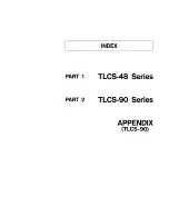
Page 5: ...INDEX PART 1 TLCS 48 Series PART 2 TLCS 90 Series APPENDIX TLCS 90 ...

Page 6: ......

Page 7: ...PART 1 TLCS 48 LSI DEVICES ...

Page 8: ......

Page 9: ... CONTENTS CONTENTS TMP8 48A TMP8035A TMP8049A TMP8039A MCU48 TMP8048A TMP80C35A 35 TMP80C49A TMP80C39A 59 TMP80C50A TMP80C40A 83 TMP8048PI TMP8035PI 107 TMP8049PI 6 TMP8039PI 6 137 TMP8243P TMP8243PI 167 TJ IP82C43P 176 MCU48 i ...

Page 10: ......

Page 11: ...capability as well as facilities for both binary and BCD arith metic The TMP 8035A TMP 8039A is the equivalent of a TMP 8048A TMP 8049A wi thout ROM program memory on chip By using this device with external EPROM or RAM software debugging becomes easy The TMP 8048AP TMP B035AP TMP 8049AP TMP 8039AP are packaged in a standard 40 pin Dual Inline Plastic Package The TMP 8048AT TMP 8035AT TMP 8049AT T...

Page 12: ...SS INT EA RD PSEN WR ALE DBa DBI DB2 DB3 DB4 DBs DB6 DB7 OV VSS EA RD PSEN WR NC ALE DBa DBI DB2 DB3 t ru Vee 5V Tl P27 P26 P2S P24 P17 P16 PIS P14 P13 P12 Pll PIa VDD SV PROG P23 P22 P21 P20 P24 P17 P16 PlS Pl4 NC PI3 P12 PlI PIa VDD Ln cr U UO 4N COCOCOCOU lZNNNNO 0000 1l41l41l41l4c Il4 MCU48 2 ...

Page 13: ...rogram counter bits during an external program mem fetch and receives the addressed instruction under the control of PSEN Also contains the address and data during an external RAM data store instruction under control of ALE RD and WR TO Input Output Input pin testable using the conditional transfer instructions JTO and JNTO TO can be designated as a clock output using ENTO CLK instruction Tl Input...

Page 14: ... en 1 rill C 1 C s en 1 enS nI til nI en nlO III c en til S nI s nI en 0 1 0 C nI III 0 C n 0 C nI I III en MCU48 4 TMP 8048A TMP 8035A TMP 8049A TMP 8039A Note Note 2 Mask ROM 1k X 8 80W 2k X 8 8049 Program Area 6 RAM r I 64 X 8 804M 128 X 8 8049 Circuit 1 2 The lower order 4 bits of port 2 output latch are used also for input out put operations with the I O expander The output latch of port o is...

Page 15: ...seful for emulation and debug and essential for testing and program verification Active High XTAL 1 Input One side of crystal input for internal oscillator Also input for external source XTAL 2 Input Other side of crystal input FUNCTIONAL DESCRIPTION 1 System Configuration 1 The following system functions of the TMP8048A are described in detail 0 Program Memory 6 Stack Stack Pointer 2 Data Memory ...

Page 16: ...ine defined by address held if in Program address 0 2047 and 2048 4095 are called memory banks 0 and 1 respec tively switching of memory banks is achieved by changing the most significant bit of the program counter PC during execution of an uncoditional jump instruction or call instruction executed after using SEL MBO or SEL MBI Reset operation automatically selects Bank O 2 Data Memory Resident D...

Page 17: ...s each having 8 bidirectional lines and 3 test inputs which can after program sequences when tested by conditional jump instructions Ports 1 and 2 are each 8 bits wide and have identical characteristics Data written to these ports is statically latched and remains unchanged unt i 1 rewri t ten As input ports these lines are non lat ching i e inputs must be present until read by an input instructio...

Page 18: ...eded Bus can serve as either a statically latched output port or a non latched input port However I O lines of this port cannot be intermixed As a static port data is written and latched using the OUTL instruction and inputted using the INS instruction these two commands generate pulses on the corresponding RD and WR strobe lines As a bidirectional port the MOVX instructions are used to read and w...

Page 19: ... count FF and overflow to Zero continuing its count until stopped by a STOP TCNT instruction or RESET The increment from maximum count to Zero overflow results in the setting of an overflow flag and the generation of an interrupt request When interrupt acknowledged a subroutine call to Location 7 will be initiated Location 7 should store the starting address of the timer or counter service routine...

Page 20: ...struction Timer Overflow R F F N TCl T 1 S Q Instruction R s Reset Instruction DIS TCNTl Instruction RETR tion r External inter CLK rupt Recognized Q CLR Execution of Inter rupt Call Instruction Fig 3 Concept of Interrupt Control Circuit 5 Interrupt Control Circuit There are two distinct types of Interrupts in the TMP8048A 1 External Interrupt from the INT terminal 2 Timer Interrupt caused by time...

Page 21: ...he counter one less than the terminal count and enabling the event counter mode A 1 to 0 transition on Tl will cause an interrupt vector to Location 7 The interrupt service routine pointed to be addresses in Location 3 or 7 must reside in memory between a and 2047 i e Bank O Figure 3 illustrates the concept of the interrupt control circuit 6 Stack Stack Pointer An interrupt or Call to subroutine c...

Page 22: ...sed for conditional jump These flags can be set reset and tested with the conditional jump instruction JFO FO is a part of the program status word PSW and is saved ln the stack area when a subroutine is called 8 Program Status Word PSW An 8 bit status word which can be loaded to and from the accumulator exists called the Program Status Word PSW The PSW is read by a MOV A PWS and written to by a MO...

Page 23: ... Bank 1 Flag 0 FO Auxiliary Carry CAC carry bit generated by an ADD instruction and used by the decimal adjust instruction DA A Ae Carry C flag which indicates that the previous opera tion has resulted in the accumulator C 9 Reset The reset input provides a means for initialization of the processor This Schmitt trigger input has an internal pullup register which in combination with an external luF...

Page 24: ...s Ports 1 and 2 to input mode Disables interrupts timer and external Stops Timer Clears Timer Flag Clears FO and Fl Disables clock output from TO 10 Oscillator Circuit TMP8048A can be operated by the external clock input in addition to crystal oscillator as shown below 5V XTAL 1 XTAL 1 XTAL Z XTAL 2 h y a Crystal Parameters and External Capacitance The frequency of the oscillator will be calculate...

Page 25: ...Max Max Max Max Max Max Max Max Max Max Max Max Max Max 10 10 10 10 15 10 20 10 20 15 15 10 20 15 25 15 25 5 to 17 5 to 15 5 to 20 5 to 17 5 to 25 5 to 20 5 to 35 5 to 17 5 to 40 5 to 25 5 to 30 5 to 20 5 to 40 5 to 25 5 to 40 5 to 25 10 to 40 b Ceramic Resonator and External Capacitance Frequency f MHz 3 to 11 1 to 3 External Capacitance Recommended Value C1 C2 pF 33 100 2 Basic Operation and Tim...

Page 26: ... access operation the following will occur The contents of the 12 bit program counter will be output on BUS DBO DB7 and the lower 4 bits of Port 2 Address Latch Enable ALE will indicate the time at which address is valid The trailing edge of ALE is used to latch the address externally Program Store Enable PSEN indicates that an external instruction fetch is in progress and serves to enable the ext...

Page 27: ...ternally 4 2 n __ In __ J n n n State ALE 400kHz P20 P23 DBC On7 ALE 1 Instruction Fetch 1 State 2 Decode 3 Execution 1 Cycle 4 Execution Next Fig 4 Instruction Cycle Timing Address Address 5 1 Execution Address Latch Timing Address L Fig 5 Timing of External Program Memory Access MCU48 17 ...

Page 28: ...rogram Address Data Address Program Address DBO DB7 InSLruction ALE RD WR I PSEN I r External Data Memory Access lnstt uctio n Suggest we have two dia rams n Write ALE r Read ALE 1 BUS BUS Data WR Fig 6 Timing of Accessing External Data Memory MCU48 18 ...

Page 29: ...of on chip I O and are addressed as Ports 4 7 All communication takes place over the lower half of port 2 P20 P23 with timing provided by an output pulse on the PROG pin Each transfer consists of two 4 bit nibbles the first containing the OP Code and port address and second containing the actual 4 bits of data 12V EA o r mET OV ALE DBO DB7 Input of Internal ROM Address J Output of Internal ROM Dat...

Page 30: ... clocking a 1 into the FF which will not appear on 55 unless ALE is high removing reset In response to 5S going high the processor begins an instruction fetch which brings ALE low resetting FF and causing the processor to again enter the stopped state The timing diagram in this case is as shown in Figure 8 b EA 5V 6 Lower Power Stand by Mode The Lower TMP8048A has been organized to allow power to ...

Page 31: ...1 I I I 1 1 1 J I r 0 1 I I I 1 IANL A iFData I 01 1 I 01 1 I 01 01 1 I 1 A A and Data 2 I 2 I I I I I d71d61dSld41d31d21dlidO I I I I ORL A Rr I ul 11 01 01 11 rl rl r A A or Rr 1 I 1 I I I I I I I I I I I I r 0 7 I I I I ORL A Rr I 01 11 01 01 01 01 01 rl A A or Rr 1 I 1 I I I I I I I I I I I I r 0 1 I I I I ORL A iFData I 01 11 01 01 01 01 11 11 A A or Data 2 I 2 I I I I d71d61dSld41d31d21dlidO...

Page 32: ...I I I I I I I I I I I p 1 2 I I I I IOUTL Pp A I al alII 11 11 al pi pi Pp A I 1 I 2 I I I I I I I I I I I I p 1 2 I I I I IANL Pp Oata I 11 al alII 11 al pi pi Pp Pp and Datal 2 I 2 I I I Id71d61d51d41d31d21dlidOI p 1 2 I I I I IORL Pp iFData I 11 01 al alII al pi pi pp Pp or Oatal 2 I 2 I I Id71d61d51d41d31d21dl1dal p 1 2 I I I INS A BUS I al al al alII al 01 01 A BUS I 1 2 I OUTL BUS A 101 al a...

Page 33: ...I 2 I 2 I I a7Ia6 a5Ia4Ia3 a2 al aOlif C 0 I I I I I I I I I I I II pc PC 2 I I I I I I I I I I I I I I Iif C 1 I I I I I IJZ Address I 11110 01011111 01 pCo 7 aO 7 I 2 I 2 I I I I I a71a61a51a41a31a21aliaOlif A 0 I I I I I I I I I I I I I I I P C p C 2 I I I I I I I I I I I I I I Iif A NEQ O I I I I IJNZ Adress I 11 01 01 11 01 11 11 01 pCO 7 aO 7 I 2 I 2 I I I I I a71a61a51a41a31a21aliaOlif A NE...

Page 34: ... I a 6 IaSI a4 Ia3 IaZ Ia 1 Ia0 I p C p SW4 7 I I 1 I I I I I 1 I SP SP 1 I I I I I I I I I I 1 PC8 10 a8 10 I I I I I I I I I I I p CO 7 a 0 7 1 I I I I I I I I I PCl1 DBF I IRET I 1 I 0 I 0 I 0 I 0 I 0 I 1 1 1 I SP SP 1 I 1 I 1 1 1 I 1 1 I I p C SP I IRETR I 11 0 I 0 I 11 0 I 0 I 11 11 SP SP 1 I 1 I 1 I I I I I 1 I I PC SP I I I I I I I I I I I PSW4 7 SP I Flag Manipulation Instruction I Mnemoni...

Page 35: ...at a I Z I Z I I I I I d71d61dSld41d31dZldlidOI r 0 1 I I I I I IMOV A PSW I 11 11 0I 0I 0I 11 11 11 A PSW I 1 I 1 I I I IMOV PSW A I 11 11 0I 11 0I 11 11 11 p SW A I 1 I 1 I I I IXCH A Rr I oI 0I 1I 0I 1I r I r I r I A Rr I 1 I 1 I I I I I I I I I I I I I I I I I I I I I I I I I I I I r 0 7 I I I I I IXCH A Rr I oI 0I 1I 0I aI 0I 0I r I A Rr I 1 I 1 I I I I I I I I I I 1 I I I I I I I I I I I I I...

Page 36: ...I I I I I I I I I I I Ievent count ing I I I I lEN TCNTI 01 01 11 01 01 11 01 11Timer interrupt 1 I 1 I I I I I I I I I I I Iis enab led I I I I IDIS TCNT1 01 01 11 11 01 11 01 11Timer interrupt 1 I 1 I I I I__________ I I I I I 1__1 ll s d is a b l ed ____ ____ I_____ I I__ 1 Control Instruction Mnemonic EN I OIS I SEL RBO SEL RB1 SEL MBO SEL MB1 ENTO CLK NOP Instruction Code I Operation 07106105...

Page 37: ... V I I______ I M W R P S EN E I__________ I I I I IVOL2 IOutput Low Voltage PROG IIOL I OmA I I 0 451 V I IVOL3 IOutput Low Voltage IIOL I 6mA I I 0 4sl V 1 I I For other output pins I I I I I I V OH I O u tp u t H i gh V o l t a ge B U S I I OH 4 0 0 u A 1 2 4 1 I V I IVOHI IOutpu Hi oltage IIOH IOOuA I 2 41 I V I I I M WR PSEN E I I I I I I V OH 2 I O u tp u t H i gh V o l t a g e I I O H 4 0 u ...

Page 38: ...DI IData InEut Read Time RD 1 I 6t 170 1 I 37S ns 1 I 1 1 1 1 1 1 1tRD2 IData InEut Read Time PSEN 1 1 4 St 170 1 I 240 ns 1 1 1 1 1 1 1 1 ItAW lAddress SetuE Time WR 1 1 St 150 1 300 I ns 1 1 1 I 1 1 I tADI IAddress SetuE Time RD I 110 St 220 I I 730 ns 1 I I I I I I tAD2 IAddress SetuE Time P SEN I I 7 St 200 1 I 460 ns I I I I tAFCI IAddress Float Time RD 1 CL 20EF 2t 40 1 1401 ns I 1 1 I tAFC2...

Page 39: ...0 r t 2 I npu t Data Hold Time I 1 5t I 01 l40 ns I P RaG I I I ItPP IPROG Pulse Width I 10 St 250 I 700 I I ns I tPL IPort2 I O Data SetuE Time ALE I 4t 2001 1601 I ns ItLP IPort2 I O Data Hold Time ALE 0 St 30 I 151 I ns I ItPV IPort OutEut Delay Time ALE I 4 5t 1001 I 5101 ns I ItOPRR 10utEut Clock Cycle Time TO I 3t I 270 I I ns I 1 Control Outputs CL 80pF BUS Output CL 150pF 2 Address Float T...

Page 40: ...MP 8048A TMP 8035A TMP 8049A TMP 8039A TIMING WAVEFORM A Instruction Fetch from External Program Memory tcy ALE BUS B Read from External Data Memory ALE RD BUS Data c Write into External Data Memory WR MCU48 30 ...

Page 41: ...rt PROG Input Enabled State TYPICAL CHARACTERISTICS t CRESET tRESET TYPICAL CURVE RESET ms 100 60 30 20 10 6 3 2 100 200 300 IOH uA v V V V V I 0 01 0 020 03 0 06 0 1 0 20 3 CRESET uF VOUT IOH TYPICAL CURVE PORT 1 2 1 2 3 4 SVOUT V V V V l IOL VOUT IOL TYPICAL CURVE rnA 40 30 20 10 10 v V V 2 3 4 VOUT IOH TYPICAL CURVE DB CONTROL 1 2 3 4 v V V MCU4B 31 5 VOUT V 5 VOUT V ...

Page 42: ...cimal digits Loading Address 4 hexadecimal digits 00 Nonnal Record Record Type 2 Digits 01 End of File Record Data Check Sum 2 hexadecimal digits Dummy characters RUBOUT BLANK before and after CR LF are optionaL Record Mark Repeated below Trailer 50 NULL characters or more 2 Example of Tape List TMP8048AP TOSHIBA MICRO COMPUTER TLCS 48 10000000066SC7D79CFSOF3F9S1FEDSSA8FF16ES70 1000100088884DDE67D...

Page 43: ... J 20 z ____________5_1 _3 f A X ________________ i 1 5 24 0 25 I J _ _ _ _ J 1 t 0 5 0 15 2 54 0 25 1 4 0 15 Note 1 This dimension is measured at the center of bending point of leads 2 Each lead pitch is 2 54mm and all the leads are located within 0 2Smrn from their theoritical positions with respect to No 1 and No 40 leads MCU48 33 ...

Page 44: ...8035A TMP 8049A TMP 8039A OUTLINE DRAWING TMP 8048AT TMP 80 35AT TMP 8049AT TMP 80 39AT PRELIMIN ARY 6 7 17 1 44 o 17 52 0 12 16 6 TYF lr l O l 40 28 39 29 I _I l O l j j Z7 TYJ f 15 76 TYP 0 MCU48 34 N o t 0 r N Unit in mm ...

Page 45: ...80C35A 6 is the equivalent of a TMP80C48A 6 without ROM program memory on chip By using this device with external EPROM or RAM software debugging becomes easy The TMP80C48AP 6 and TMP80C35AP 6 are 1n a standard Dual Inline Package The TMP80C48AF 6 is in a 44 pin Flat Package The TMP80C48AT and TMP80C35AT are packag d in the JEDEC standard type 44pin PLCC p las t ic Leaded Ch ip Carrier FEATURES TM...

Page 46: ...8AF 6 TMP80C48AT TMP80C35AT PROG P23 P22 P21 P20 NC Vss DB7 DBB D D MCU48 36 1 0 39 38 37 36 35 34 33 32 31 30 29 28 27 26 25 21 23 22 21 NT EA jffi PSEI WR NC ALE DBO DBI DB2 DB3 VCC SV T P27 P26 P2S P2 P17 Plb f 15 P1a Pl3 P12 Pll o PROG P23 P22 1 21 P20 PLCC r J J tr l 0 r c Itr l loW f f co U u N N N tr la i oz f e e e oil S 4 1 2 1 10 0 2 oC 0 1 oJ a __ l _ P24 L l PI7 P16 li PIS li Pl4 NC PI...

Page 47: ...ROG CIl tl CIlt 3 c CIlt 3 CIlOJ t 0 rh Z z t 3 1 Sis 001 Z oo tI t t 3 Z 1 c O tIO t 3 5 tIQ o c oQ c 0 c t t t 3 tI1 0 tJ l Z t Z t 3 OJ tI1 t 31 OJt c CIlOJ l 3s l 3 l 3 Z 0 t CIl c tI c g c 0 I tI1 I l 3 c b5 C I l Note 1 The lower order 4 bi t of port 2 output lat ch are used al so for input output operations with the I O expander Note 2 The output latch of port a is also used for address out...

Page 48: ...8 low order program counter bi ts during an external program memory fetch and receives the addressed instruction under the control of PSEN Also contains the address and data duri an external RAM data store inst ruction under control of ALE RD and WR TO Input Output Input pin testable using the conditional transfer instructions JTO and JNTO TO can be designated as a clock output using ENTO CLK inst...

Page 49: ...ch to external program memory Active Low SS Input Single step input can be used in conjunction with ALE to single step processor through each instruction when SS is low the CPU is placed into a wait state after it has completed the instruction being executed Also used during the power down mode EA Input External Access input which forces all program memory fetches to reference external memory Usef...

Page 50: ...OnIc OUll PP A Object Cooc 1st function 2m Bin lex 00111000 38 0 Pp IA P 1 2 A HC liJ n OM10jip 98 p pp Po i 1 Z I liiliiii ii N O itC lp r 1000100p 884 p pp Pp V I P 2 P Iii iii ii ii U 1MS A 8Ii f 00001000 08 TA 81 i T OUT Bu i A 00000010 02 BUS IAt f o U r B tij i 1 0011 000 00 8OS BUSl t T i liii iii i i PORC 8 05 10001000 88 8 i f 8IJSl vi U _ _ i i IJi iJi Ii I T Flaq Ie C AC 2 z i 2 2 2 f I...

Page 51: ...truction 3 flaG Instruct on ft IMtnJttlon h 1 l Assembler Ie alii Hoe onle HOV Rr i H HOV itr r o v t lV PS r eHOV Psw A XCH A Rr XC A Rr n XCtlD A Rr S t VX Rr A t HOVX A Rr TC io IIIJ en rt 0 r HOVP A HOvpj A A HOV A 1 t V T A STR STRT Off STOP TCHT IN TCHTI OIS lCKTJ Object Code 1st 2M Bin lex 10111rrr 88 r iii i Ii i i ii 1011000r 804r iii iii i i j 11000111 C7 11010111 07 00101rrr 2R r 00lOO0...

Page 52: ...ci 1 1 I 1VOL 10utput Low Voltage IOL 1 6mA 1 1 1 0 4sl v 1 1 1 Except PlO P17 P20 P27 1 1 1 1 1 IVOL1 10utput Low Voltage IOL 1 2mA 1 1 1 0 4sl v 1 I 1 PlO P17 P20 P27 1 1 1 1 1 IVOHll 10utput High Voltage IOH 1 6mA I I I I v I I I Except P 10 P 17 P 20 P 27 I I I I I IVOH12 10utput High Voltage IOH 400 A Ivcc I I I v I 1 I Except PlO P17 P20 P27 I O BI I I I IVOH2l 10utput High Voltage IIOH SO A...

Page 53: ...l IData Input Read Time I 15 5t 120 I 375 ns I I RD I I I I tRD2 IData Input Read Time I I 4t 120 I 240 ns I I PSEN I I I I tAW IAddress Setup Time I I 5t 150 I 300 ns I I WR I I I I tADI IAddress Setup Time I I 10t 1701 730 ns I I RD I I I I tAD2 IAddress Setup Time I I 7t 170 I 460 ns I I PSEN I I I I tAFCllAddress Float Time ICL 20pF I 2t 40 I 140 ns I RD z WR I I I tAFC21Address Float Time CL ...

Page 54: ...P1 llse Width 110 st 2s0 700 I ns I tPL IPort 2 I O Data SetuE Time ALE I I 4t 200 I 160 I I ns I tLP IPort 2 I O Data Hold Time ALE I 10 st 30 I 15 I I ns I tPV IPort OutEut Dela Time ALE I 14 st l00 I I 510 I ns I tOPRR ITO Clock Period I I 3t I 270 I I ns I tCY IC ycle Time I I 15t I 1 36115 0 I l ls Note 1 Control Output CL 80pF BUS Output CL ls0pF 2 The f t assumes 50 duty cycle on XTALI and ...

Page 55: ...O ll VCC v I 1 XI ALI XI AL2 RESET PS I Ix vcci 1 I IVOL 10utput Low Voltage IIOL 1 6mA 1 1 0 451 v 1 1 1 Except PIO PI7 P20 P27 1 1 I IVOLI Output Low Voltage IIOL I 2mA 1 0 4sl v 1 I 1 PlO P17 P20 P27 1 1 I 1 1 VOHll 10utput High Voltage IIOH l 6mA I I I v I I I Except PlO P17 P20 P27 I 1 VOH12 10utput High Voltage IIOH 400 A Ivcc I I I v I Except PIO PI7 P20 P27 I I 0 81 1 I IVOH2l 10utput High...

Page 56: ...ut Low Voltage IOL 1 2mA 1 0 451 v 1 1 PlO PI7 P20 P27 I I IVOH12 10utput High Vol tage IIOH 40011A 1VCC I V Except P 10 P 17 P 20 P 27 I 0 sl I 1 IVOH22 Output High Voltage IIOH 25llA Ivcc I I v I I 1 PlO P17 P20 P27 I I o SI I I I IILI Input Leak Current IVSS VIN VCC 1 I TOlliAl I I T 1 INT EA Ps I I I 1 ILl 1 I E ut Leak Current IVSS VIN VCC I I I vcc IliA I I I SS RESET I I I 0 1 IILl 2 IInput...

Page 57: ...Read Time I I 4t 120 I I 550 I ns I I p SEN 1 I I 1 I 1 tAW IAddress Setup Time I St 150 I 680 I I ns I I WR I I I tADl Address Setup Time I I 10t 1701 11500 1 ns I I RD I I I I tAD2 IAddress Setup Time I I 7t 170 I 11000 I ns I I P SEN 1 I I I I tAFCl Address Float Time ICL 20pF I 2t 40 I 290 I I ns I I RD WR 1 1 1 I I I tAFC21Address Float Time I CL 20pF 10 5t 40 1 40 1 I ns I I p SEN 1 1 1 1 1 ...

Page 58: ... Width 1 110 St 2SoI1S00 I I ns 1 tPL IPort 2 I O Data SetuE Time ALE 1 1 4t 200 1 460 I 1 ns I tLP IPort 2 I O Data Hold Time ALE 10 St 30 1 130 1 I ns I tPV IPort OutEut Dela Time ALE I 14 5t 100 I I 850 I ns I tOPRRITO Clock Period I 1 3t 1 500 1 I ns I t C l ICvcle Time I I 1St I 2 5 115 0 I llS Note 1 Control Output CL 80pF BUS Output CL lS0pF 2 The fet assumes 50 duty cycle on XTAL1 and XTAL...

Page 59: ... TMP 80 C48AP 6 TMP80 C35AP 6 TMP80 C48AF 6 TMP80C48AT TMP80C35AT A Instruction Fetch from External Program Memory ALE PSEN DBO 7 INSTRUCTION B Read from External Data Memory ALE I tccl I DBO 7 INPUT DATA _____ tADI MCU48 49 ...

Page 60: ...80 C48AF 6 TMP80C48AT TMP80C3SAT C Write into External Data Memory CAl 1 D Timing of Port 2 during Expander Instruction Execution ALE CAl PORTl 2 PORT 1 2 DATA NEW PORT 1 2 DATA PORT 20 23 PORT 20 23 DATA PCH PORT 20 23 pORT 20 23 DATA PCH PROCi MCU48 S0 ...

Page 61: ...P R O C to 70 C VS S OV TMP80C48AP 6 3SAP 6 TMP80C48AF 6 TOPR 40 C to 8S C VSS OV SYMBOL I PARAMETER TEST CONDITION MIN TYP MAX UNIT 1 1 1 1 VSBl 1 Standby Voltage l 1__________ 1 2 0 1 6 0 1 V 1 1 1 IVCC SV VIH VCC 0 2V 1 1 1 1 1 1 ISBl 1 Standby Current l IVIL 0 2V 1 1 0 5 I 10 1 lJA 1 AC CHARACTERISTICS TMP 80 C48AP 3SAP TMP80C48AF TMP 80 C48AT 3SAT TOPR O C to 70 C VSS OV TMP80C48AP 6 3SAP 6 T...

Page 62: ...C to 70 C VSS OV TMP80C48AP 6 3SAP 6 TMP80C48AF 6 TOPR 40 C to 85 c VSS OV 1SYMBOL 1 PARAMETER 1 TEST CONDITION I MIN I TYP I MAX I UNIT I I I I I I I I 1 1 VSB2 1 Standby Voltage 2 1 __________ 1 3 0 1 1 6 0 1 V 1 1 1 IVCC SV VIH VCC 0 2V 1 1 1 1 1 I ISB2 1 Standby Current 2 IVIL 0 2V I I 0 5 I 10 1 A 1 AC CHARACTERISTICS TMP80C48AP 3SAP TMP80C48AF TMP80C48AT 35AT TOPR O C t070 C VSS 5V 10 VSS OV...

Page 63: ...the following table 4 Release from HALT MODE HALT MODE is released by either of two signals RESET INT 1 RESET Release Mode An active RESET input si gnal causes the normal reset function TMP80C48A TMP80C35A start the program at address 000 H 2 INT Release Mode An active INT input signal causes the normal oper ation In case of interrupt enable mode EI MODE TMP80C48A TMP80C35A execute the interrupt s...

Page 64: ...IIHigh II Leve 1 Input disabled when oscillator is stopped Pull up transistors turn off Input disabled when oscilltor is stopped High impedance PIN STATUS IN HALT MODE PIN NAME DBO DB7 PlO Pl7 P20 P27 TO Tl XTALl XTAL2 RESET INT SS EA RD WR_ _ PROG PSEN ALE STATUS Values prior to the execution of HALT INSTRUCTION are maintained Status prior to the execution of HALT INSTRUCTION is maintained Input ...

Page 65: ...V TMP80 C48AP 6 TMP80C35AP 6 TMP80C48AF 6 TMP80C48AT TMP80C35AT 30pF 20pF IOOpF 30pF Ta 25 C IOL rnA 40 30 20 10 50 100 150 C2 unless otherwise noted VOUT IOL TYPICAL CURVE V 1 2 3 4 VOUT IOH TYPICAL CURVE PORT 1 2 1 2 3 4 5 VOUT V v V 5 10 200 IOH 15 fXTAL MHz uA t CRESET tRESET TYPICAL CURVE RESET ms 100 60 30 20 10 6 3 2 0 0 v V 5 V 10 15 0 020 03 0 06 0 1 0 2 0 3 C uF IlESET 20 IOH mA MCU48 55...

Page 66: ... 3 M A X __________________ i 15 24 0 25 Note 1 2 J 0 5 0 15 2 54 0 25 ____ J t i t U O 25 0 1 0 05 1 4 0 15 0 15 This dimension is measured at the center of bending point of leads Each lead pitch is 2 54mm and all the leads are located within O 25mm from their theori tical pos i t ions wi th respe ct to No 1 and 1 1_ I n 1 __ 3_ MCU48 56 ...

Page 67: ...35AT OUTLINE DRAWING FLAT PACKAGE I l4 3 l I I 36 I I 7 38 39 a 41 I 4 3 CO 0 7 J fl o 35 0 8 pitch t f J I i I _ _ t Z II 4J I 2 iJ lEl J 16 0 t 0 1 0 16 15 l 1 3 l2 i 14 0 O 1 16 9 MARK C iJUUUUJJUUUUU lS 2 tO 3 MCU48 57 1 45 o 3 f 1 1 0 85 0 3 N 0 i U I t o N Unit in mm ...

Page 68: ...BA TMP 80C48AP 6 TMP 80C35AP 6 TMP 80C48AF 6 TMP80C48AT TMP80C35AT OUTLINE DRAWING Plastic Leaded Chip Carrier 6 1 44 40 7 o 39 17 29 28 17 52 0 12 I _H l O 1 jl 27TYj I 15 76 TYP MCU48 58 o U r unit in rom ...

Page 69: ... is the equivalent of a TMP80C49A 6 without ROM program memory on chip By using this device with external EPROM or RAM software debugging becomes easy The TMP80C49AP 6 and TMP80C39AP 6 are in a standard Dual Inline Package The TMP80C49AF 6 is in a 44 pin Flat Package The TMP80C49AT and TMP80C39AT are packaged in the JEDEC standard type 44pin PLCC Plastic leaded Chip Carrier FEATURES TMP80C49AP TMP...

Page 70: ...PROG P23 P22 P21 P20 He Vss DB7 DB6 DB5 D TMP80C49AP 6 TMP80C39AP 6 TMP80C49AF 6 TMP80C49AT TMP80C39AT VCC SV T P27 P26 P25 P2 P 7 P16 f 1S Pl Pl 3 P12 Pll O PROG P23 P n P 21 P20 PLCC r tI 0 111 oJ f f CI 0 0 N N N 1I a l Z f c c c oil S 4 3 2 1 4 l3 062 11 40 LJ I t t J NT r P24 EA It P17 RD P16 PSEN X PIS Wit l i PH NC NC ALE if Pl3 DBO P12 DBl 2 Pll DBl iC PIO DB3 Ps g c Ic Ic Ic I MCU48 60 ...

Page 71: ... lower order 4 bit input output operations to 0 l 68 tr t t s of with TMP BOC49AP 6 TMPBOC39AP 6 TMPBOC49AF 6 TMPBOC49AT TMPBOC39 T tr e l l 0 tr I tr INSTRUC T ION RE GIST EF DECODER ACC J1fJLATOf Ell TEST H I e 0 tr Z I e I r port 2 output latch the I O expander are used RA1 128x 6 also for Note 2 The output latch of port o is also used for address output MCU4B 61 ...

Page 72: ...he 8 low order program counter bits during an external program memory fetch and receives the addressed instruction under the control of PSEN Also contains the address and data duri an external RAM data store inst ruction under control of ALE RO and WR TO Input Output Input pin testable using the conditional transfer instructions JTO and JNTO TO can be designated as a clock output using ENTO CLK in...

Page 73: ...ch to external program memory Active Low SS Input Single step input can be used in conj unction wi th ALE to single step processor through each instruction when SS is low the CPU is placed into a wait state after it has completed the instruction being executed Also used during the power down mode EA Input External Access input which forces all program memory fetches to reference external memory Us...

Page 74: ...TLCS 8 LIST OF tHSTRttTl JfS 214 I Ic AsseMbler Object Code Ip 1st runction FIi19 Ie i1 HncllOnic f M lfIJ rs B in lIc x r ______ rC _AC OIlTl Po A 00111000 J8 0 Po A P 1 2 2 A HC PIJ I I 10 Oll0 Pj 98 0 Pri Pp i iii II iii ii 10001000 88 0 liiiiiii NORC jiilr p U r I o U r p u T MS if 8 00001000 OIlTC SUS A 00000010 iii i i ii i o iif sUs lf 10001000 iiliiiii ii 08 TA Sitc 1 02 BUS ACl ii 88 SUSf...

Page 75: ...uct Ion ft Instrvct Ion TLCS 48 LIST or INSTRllCTJONS 414 I rc Assembler Object Code Ie 1st runet ion all Hnellonlc 200 S Bin HOV Rr i 10111rrr iiiiiiii H HOV Rr 1011000r 0 iii iii ii v r 1 PSi 11000111 HOV PSW A 11010111 c XCH A Rr 00101rrr XCH A lIRr 0010000r n XCIID A flRr 0011000r s HOVX Rr A 1001000r t HOVX A flRr 1000000r HOVp A flA 10100011 HOVP j A A 11100011 TC HOV A l 01000010 io HOY T A...

Page 76: ...0utput Low Vol tage IOL l 6mA 1 1 1 0 4sl v I I ExceEt PlO P17 P20 P27 I I I I IVOLI 10utput Low Voltage IOL l 2mA 1 1 1 0 4SI v I I PIO PI7 P20 P27 I I I I IVOHll 10utput High Voltage IOH 1 6mA 12T1 I I v I I ExceEt P10 P17 P20 P27 I I I I IVOH12 10utput High Voltage IOH 40011A Jvcc I I I v I I Except PIO PI7 P20 P27 I o SI I I IVOH21 10utput High Voltage IOH SOllA 12T1 I I v I I p 10 P 17 P 20 P...

Page 77: ...e I PSEN tCAl IControl to ALE Time I RD WR PROG tCA2 IControl to ALE Time I PSEN t CP IPort Control Setup Time PROG tPC IPort Control Hold Time PROG tPR IPort 2 Input Data Setup Time I PROG tPF IPort 2 Input Data Hold Time I PROG tDP IPort 2 Output Data Setup Time I PROG tPD IPort 2 Output Data Hold Time I PROG unless otherwise noted ITEST I f t ICONDITION I I 11 MHz IUNIT MAX I INote 2 I l xtal f...

Page 78: ...Pulse Width I IlO St 2501 700 I I ns I tPL IPort 2 I O Data SetuE Time ALE I I 4t 200 I 160 I I ns I tLP IPort 2 I O Data Hold Time ALE I 10 St 30 I 15 I I ns I tPV IPort OutEut Delay Time ALE I 14 5t lOO 1 1 510 1 ns I tOPRR ITO Clock Period 1 1 3t I 270 I I ns I tCY IC z cle Time I 1 1St I 1 36115 0 1 llS Note 1 Control Output CL 80pF BUS Output CL lSOpF 2 The f t assumes 50 duty cycle on XTAL1 ...

Page 79: ...I Ix vcci I I I IVOL 10utput Low Voltage IIOL 1 6mA 1 1 1 0 4SI v 1 I I ExceEt P 10 P 17 P 20 P 27 I I I I I I IVOLI 10utput Low Voltage IIOL l 2mA 1 1 1 0 451 v 1 I I PIO P17 P20 P27 I I I I I I IVOHll IOutput High Voltage IIOH I 6mA I I I I v I I I ExceEtPlO PI7 P20 P27 I I I I I I IVOHl2 10utput High Voltage IIOH 40011A IVCC I I I v I I I ExceEt PIO P17 P20 P27 I I o BI I I I IVOH21 10utput Hig...

Page 80: ...IOL 1 6mA 1 1 1 0 451 v 1 ___ I Except P 10 P 17 P ZO P 27 I 1 I VOLI IOutput Low Voltage IOL l 2mA 1 1 1 0 4SI v 1 PlO P17 PZO PZ7 I I I I I VO H l Z IOutput High Voltage IIOH 400 A Ivcc I I I v I ___ I Except PlO P17 P20 PZ7 I 0 81 I I I VOH22 IOutput High Voltage IIOH 2s A Ivcc I I I v PlO P17 P20 P27 1 0 8 ILl Input Leak Current VSS VIN VCC 1 1 10 Tl INT EA PS I IL I l I I p ut Leak Current VS...

Page 81: ... I tRDl I Data Input Read Time I Is st 120 I 800 I ns I I RD I I I I I tRD2 IData Input Read Time I I 4t 120 I 550 I ns I I PSEN I I I I tAW IAddress Setup Time I 5t 150 680 I I ns I I WR I I I I tADl IAddress Setup Time I 10t 170 11500 I ns I I RD I I I I tAD2 IAddress Setup Time I 7t 170 11000 I ns I I PSEN I I I I tAFC11Address Float Time CL 20pF I 2t 40 290 I I ns I I RD WR I I I tAFC21Address...

Page 82: ...se Width I 110 st 2s0 11500 I I ns I tPL IPort 2 I O Data SetuE Time ALE I I 4t 200 I 460 I I ns I tLP IPort 2 I O Data Hold Time ALE I 10 st 30 I 130 I ns I tPV IPort OutEut Delay Time ALE I 14 st l00 I I 850 ns I tOPRR TO Clock Period I I 3t I 500 I I ns I tCY IC icle Time I I 1St I 2 5 115 0 I s Note 1 Control Output CL 80pF BUS Output CL ls0pF 2 The f t assumes 50 duty cycle on XTALI and XTAL2...

Page 83: ...C49AP 6 TMP80C39AP 6 TMP80C49AF 6 TMP80C49AT TMP80C39AT TIMING WAVEFORM A Instruction Fetch from External Program Memory ALE PSEN DBO 7 B Read from External Data Memory ALE tcc1 DBO 7 INPUT DATA _____ IAD1 MCU48 73 ...

Page 84: ...C49AT TMP80C39AT C Write into External Data Memory ALE DBO 7 OUTPUT DATA D Timing of Port 2 during Expander Instruction Execution ALE CAl PORTl 2 PORT 1 2 DATA NEW PORT 1 2 DATA PORT 20 23 PORT 20 23 DATA PCH PORT 20 23pORT 20 23 DATA PCH PROCi MCU48 74 ...

Page 85: ...ss 0 DC CHARACTERI STI CS TMP80C49AP 39AP TMP80C49AF TMP80C49AT 3SAT TOPR O C to 70 C VSS OV TMP80C49AP 6 39AP 6 TMP80C49AF 6 TOPR 40 C to 8S C VSS OV SYMBOL PARAMETER TEST CONDITION MIN TYP MAX UNIT I I I I I VSBI Standby Voltage l 2 0 6 0 V V CC SV V IH V C C 0 2V ISBI Standby Current l VIL 0 2V 0 5 10 lJA AC CHARACTERISTICS TMP80 C49AP 39AP TMP80C49AF TMP80C49AT 39AT TOPR O C to 70 C VCC 5V 10 ...

Page 86: ...V TMP80C49AP 6 39AP 6 TMP80C49AF 6 TOPR 40 C to 8S C VSS OV 1SYMBOL 1 PARAMETER 1 TEST CONDITION 1 MIN 1 TYP 1 MAX 1 UNIT 1 I I I I I I I I I VSBZ I Standby Voltage Z I I 3 0 I I 6 0 1 V I I I I vc c SV V IH V C C O zv I I I I I I ISBZ 1 Standby Current 2 IVIL 0 2V I I O S I 10 1 llA I AC CHARACTERISTICS TMP80 C49AP 39AP TMP 80C49AF TMP 80C49AT 39AT TOPR O C to 70 C VSS SV 10 VSS OV TMP80C49AP 6 3...

Page 87: ...e following table 4 Release from HALT MODE HALT MODE is released by either of two signals RESET INT 1 RESET Release Mode An active RESET input signal causes the normal reset function TMP80C49A TMP80C39A start tne program at address 000 H 2 INT Release Mode An active INT input signal causes the normal oper ation In case of interrupt enable mode EI MODE TMP80C49A TMP80C39A execute the interrupt serv...

Page 88: ...h Level Input disabled when oscillator is stopped Pull up transistors turn off Input disabled when oscilltor is stopped High impedance PIN STATUS IN HALT MODE PIN NAME DBO DB7 PIO Pl7 P20 P27 TO TI XTALl XTAL2 RESET INT SS EA RD WR PROG PSEN ALE STATUS Values prior to the execution of HALT INSTRUCTION are maintained Status prior to the execution of HALT INSTRUCTION is maintained Input disabled Con...

Page 89: ...unless Otherwise noted VCC fMAX TYPICAL CURVE VCC V 6 5 4 3 ICC rnA 10 5 v V 5 10 15 fXTAL MHz fXTAL ICC TYPICAL CURVE V 5 10 15 fXTAL MHz t CRESET tRESET TYPICAL CURVE RESET ms 100 60 30 20 10 6 3 2 V o 0 020 03 0 06 0 1 0 2 0 3 C uF RESET IOL rnA 40 30 20 10 50 100 150 200 IOH uA 5 10 15 20 IOH mA MCU48 79 VOUT IOL TYPICAL CURVE i V 2 3 4 V OUT IOH TYPICAL CURVE PORT 1 2 1 2 3 4 5 VOUT V 5 VOUT ...

Page 90: ...1 c N 20 ____________ 5 1 3 M A X P__________________ i 15 24 0 25 J 0 5 0 15 2 54 0 25 1 4 0 15 0 1 Note 1 This dimension is measured at the center of bending point of leads 2 Each lead pi tch is 2 S4mm and all the leads are located within O 2Smm from their theoritical positions with respect to No 1 and No 40 leads MCU48 80 ...

Page 91: ...GE o 35 I 0 8 pitch H I I l I I 3 3 i 3 2 t l b 6 2 i c 34 I I 3 I 36 a 7 I 1P P 4 1 38 MARKING t 16 0 0 39 AREA I 1 0 I I 0 16 f I P 4 I IT 41 15 1 L L 3 1 2 14 I 1 l 3 I 12 CO 1 2 3 t 6 9 0 11 Ut t I t t t t l I I 7 1 0 14 0 t O l 16 9 MARK 1 4S O 3 E C J C f o U N e N 15 2 0 3 0 85 31 MCU48 81 ...

Page 92: ...C49AP 6 TMP 80C39AP 6 TMP80C49AF 6 TMP80C49AT TMP80C39AT OUTLINE DRAWING Plastic Leaded Chip Carrier 6 I 44 40 7 o 17 28 17 52 0 12 39 29 N c LI r r 16 6 TYP O 71 tO 1 i I O O l ypt 15 7bTYP I MCU48 82 N c unit in mm ...

Page 93: ... the equivalent of a TMP80CSOA 6 without ROM program memory on chip By using this device with external EPROM or RAM software debugging becomes easy The TMP80CSOAP 6 and TMP80C40AP 6 are in a standerd Dual Inline Package The TMP80CSOAF 6 is in a 44 pin Flat Package The TMP80CSOAT and TMP80C40AT are packaged in the JEDEC standard type 44pin PLCC Plastic Leaded Chip Carrier FEATURES TMP80CSOAP TMP80C...

Page 94: ...B5 os TMP80 CSOAP 6 TMP80 C40AP 6 TMP 80CSOAF 6 TMP80CSOAT TMP80C40AT 4O VCC 5V 39 11 38 P27 37 P26 36 P25 35 P2 34 PI7 33 Pl6 32 Fl S 31 P1 30 Pl 3 29 P12 28 Pll 27 O 26 25 PROG 24 P 3 23 P22 22 P21 21 P20 PLCC r oJ Ir 0 oJf f COU I lNN ce f oZ f c c c S 4 3 2 Il III oC 1 40 L I r rI of NT PZ4 EA 3 P17 iD I_ f P16 PSER J l P1S WR ki P14 NC NC ALE P13 DBD P12 DBl l Pll DBZ P10 DB3 t Ps g QQQQ MCU4...

Page 95: ...S T RD WR PROG 1 11 1 OJ 1 3 OJ OJ OJ 0 tr l1 3 1 10 t zz 1 3 o OJt 1 ZOJ OJ t Z t 1 68 0 1 3 l ll l 0 0 0 c 0 0 t e o 0 tl lz t z l l l l e 1 3t 1 ca 1 1 c OJCJ r l 3 1 3 Z t OJ 0 0 c E 0 tr t 1 l l th OJ Note 1 The lower order 4 bit of port 2 output latch are used also for input output operations with the I O expander Note 2 The output latch of port 0 is also used for address output MCU48 85 ...

Page 96: ... 8 low order program counter bi ts during an external program memory fetch and receives the addressed instruction under the control of PSEN Also contains the address and data duri an external RAM data store inst ruction under control of ALE RD and WR TO Input Output Input pin testable using the conditional transfer instructions JTO and JNTO TO can be designated as a clock output using ENTO CLK ins...

Page 97: ...fetch to external program memory Active Low SS Input Single step input can be used in conjunction with ALE to single step processor through each instruction when SS is low the CPU is placed into a wait state after it has completed the instruction being executed Also used during the power down mode EA Input External Access input which forces all program memory fetches to reference external memory U...

Page 98: ... _ _ _ _ TLCS 8 LIST Of tNSTRttTlIJfS 214 I 1 ASSeMbler Object Code 1st 2nd Ie 11 5 funct ion HnelllOnic 8in lip x OUTL PP A 0011100p JIJ p Pot t A _ AHC p p n I 00110 00 M p pp Pp i Ii II Ii ii I N ORC p ii lr 10001000 88 0 fpp Pp V i II iii iii i i p U T I o U T p U T lNS r 8Iiifoooo1000 OS TA 8i f O UTC Bi1i A 00000010 02 BUS t AC iiiiiiii ORr 8 05 10001000 iiiiiiil ii 88 B f 8US vi Ii FIiJ9 Cy...

Page 99: ...Instruct Ion fl M M InslMICt Ion TlCS 48 LIST or J STRttlJONS M4 1 Assembler Ie m HneIRonlc HOV Rr i Object Code 1st 2M Bin lex 10111rrr B8 r Rr o j iii iii iii i H HOv liir r 1011000r 80 r nRr l i o iii iii jiii V H jii l psifH 11000111 C1 A IPSW e HOV PsW A 11010111 07 IPSW AI rUllCt ion r 0 7 XCii A Rr 00101rrr 211 r A Ilr rt O 1 XCii A lIRr 001OOOOr 20 r A Rr r O 1 I XClID A lRr 0011000r 30 r ...

Page 100: ... PS I vcc 1 I I 1 IVOL IOutput Low Voltage IOL I 6mA 1 1 0 451 v 1 1 Except PlO PI7 t P20 P27 1 1 1 IVOLI IOutput Low Voltage IOL I 2mA 1 1 0 451 v 1 I 1 PIO PI7 P20 P27 I 1 I 1 IVOHll IOutput High Voltage IOH l 6mA 12 41 I I v 1 1 1 Except PIO PI7 P20 P27 1 1 1 I IVOHl2 Output High Voltage IOH 400 lA Ivcc I I v I Except PIO PI7 P20 P27 O S 1 1 1 1VOH21 Output High Vol tage IOH 50 lA 12 41 I v 1 1...

Page 101: ...15 5t 120 I 375 ns I I I RD I I I I I tRD2 IData Input Read Time I I 4t 120 I 240 ns I I I p SEN I I I I tAW IAddress Setup Time I I 5t 150 I 300 ns I WR I I I tAD1 IAddress Setup Time I I 10t 1701 730 ns I I I RD I I I I I tAD2 IAddress Setup Time I I 7t 170 I 460 ns I I I PSEN I I I I I tAFC1 Address Float Time ICL 20pF I 2t 40 I 140 ns I I I RD WR I I I I I tAFC21Address Float Time ICL 20pF 10 ...

Page 102: ...IPROG Pu lse Width I IIO St 2Sol 700 I I ns I tPL IPort 2 I O Data SetuE Time ALE I I 4t 200 I 160 I I ns I tLP IPort 2 I O Data Hold Time ALE I 10 St 30 I 15 I I ns I tPV IPort Out ut Dela Time ALE 1 4 St l00 1 510 1 ns I tOPRRITO Clock Period 1 3t 1 270 1 1 ns 1 tCY IC tcle Time 1 1 1St 1 1 36115 0 1 llS Note 1 Control Output CL 80pF BUS Output CL IS0pF 2 The f t assumes 50 duty cycle on XTALI a...

Page 103: ... RESET PS I I VIHl Input High Volt _ I VCCI v 1 I XTALl XTAL2 RESET PS I x vcc I I IVOL Output Low Voltage IOL 1 6mA 1 0 4s V Except P 10 P 17 P 20 P 27 I I I IVOLl Output Low Voltage IOL l 2mA r I 0 4SI v I I PlO P17 P20 P27 I I I IVOHl 10utput High Voltage IOH l 6mA 12 4 I v 1 Except PIO PI7 P20 P27 I I I I VOH12 Output High Voltage IIOH 40011A Ivcc I v Except PIO P17 P20 P27 I o BI I I I IVOH2l...

Page 104: ... 1__ 1__ IVOLI IOutput Low Voltage IOL l 2mA I I 10 4SI V I I PIO P17 P20 P27 1__ 1 __ 1_ _ 1__ I OH12 IOutput High Vol tage IOH 400llA IVCC I I I V I I Except PlO P17 P20 P27 I I __ I__ I__ IVOH22 IOutpt lt High Voltage IOH 2SllA Ivcc I I I V I I PIO P17 P20 P27 I 0 81 I I ILl IInput Leak Current VSS VIN VCC 1 I I i O IliA I Tl ffi EA PS 1__ 1__ 1_ _ 1__ ILl 1 II ut Leak Current IVSS VIN VCC I I ...

Page 105: ...Dl Data Input Read Time 5 5t 120 I I 800 ns I RD I I I tRD2 Data Input Read Time 4t 120 I I 550 ns I PSEN I I tAW Address Setup Time 5t 150 I 680 I ns WR I I tADl Address Setup Time 10t 1701 11500 ns RD I I tAD2 Address Setup Time 7t 170 I 1000 ns p SEN I tAFCl Address Float Time CL 20pF 2t 40 I 290 ns RD WR I tAFC21Address Float Time CL 20pF 10 5t 40 I 40 ns I I p SEN ItLAFC11ALE to Control Time ...

Page 106: ...Pulse Width I IIO st 2s011s00 I I ns I tPL IPort 2 I O Data SetuE Time ALE 1 1 4t 200 1 460 1 1 ns I tLP IPort 2 I O Data Hold Time ALE 1 10 st 30 1 130 1 I ns 1 tPV IPort Out ut Dela Time ALE 1 14 st l00 1 1 850 1 ns 1 tOPRRITO Clock Period 3t 500 1 I ns 1 tC f IC icle Time 1 1St 2 5 115 0 1 llS Note 1 Control Output CL 80pF BUS Output CL ls0pF 2 The f t assumes 50 duty cycle on XTALI and XTAL2 T...

Page 107: ...G WAVEFORM TMP80CSOAP 6 TMP80 C40AP 6 TMP80 CSOAF 6 TMP80CSOAT TMP80C40AT A Instruction Fetch from External Program Memory ALE PSEN DBO 7 1 tADZ B Read from External Data Memory ALE DBO 7 INPUT DATA t tADI MCU48 97 ...

Page 108: ... TMP80C40AT c Write into External Data Memory tCAl ALE tcel tDW DBO 7 OUTPUT DATA D Timing of Port 2 during Expander Instruction Execution ALE tpv CAl PORTl 2 PORT 1 Z DATA NEW PORT 1 2 DATA PORT 20 23 PORT ZO Z3 DATA PCH PORT 20 23pORT 20 23 DATA PCH PRoe MCU48 98 ...

Page 109: ...CSOAP 40AP TMP80CSOAF TMP80CSOAT 40AT TOPR O C to 70 C VSS OV TMP80CSOAP 6 40AP 6 TMP80CSOAF 6 TOPR 40 C to 8S C VSS OV 1SYMBOL 1 PARAMETER I TEST CONDITION 1 MIN 1 TYP 1 MAX 1 UNIT 1 I I I I I I VSBI 1 Standby Voltage l 1 1 2 0 1 1 6 0 V I vc c SV V IH V C C 0 2V I I I 1 ISBI 1 Standby Current l VIL 0 2V 1 1 0 5 1 10 1 UA AC CHARACTERISTICS TMP80C50AP 40AP TMP80CSOAF TMP80C50AT 40AT TOPR O C to 7...

Page 110: ...ACTERISTICS TMP80CSOAP 40AP TMP80CSOAF TMP80C50AT 40AT TOPR O C to 70 C VSS OV TMP80CSOAP 6 40AP 6 TMP80C50AF 6 TOPR 40 C to 85 C VSS OV ISYMBOL I PARAMETER I TEST CONDITION I MIN I TYP I MAX I UNIT I I I I I I I VSB2 Standby Voltage 2 3 0 I 6 0 V I VC C 5V V IH V C C 0 2V I ISB2 Standby Current 2 IVIL 0 2V 0 5 10 llA I AC CHARACTERISTICS TMP80CSOAP 40AP TMP80CSOAF TMP80C50AT 40AT TOPR 0 C to 70 C...

Page 111: ...ollowing table 4 Release from HALT MODE HALT MODE is released by either of two signals RESET INT 1 RESET Release Mode An active RESET input signal causes the normal reset function TMP80C50A TMP80C40A start the program at address 000 H 2 INT Release Mode An active INT input signal causes the normal oper ation In case of interrupt enable mode EI MODE TMP80C50A TMP80C40A execute the interrupt service...

Page 112: ...t High Level Input disabled when oscillator is stopped Pull up transistors turn off Input disabled when oscilltor is stopped High impedance PIN STATUS IN HALT MODE PIN NAME DBO DB7 PIO P17 P20 P27 TO Tl XTALl XTAL2 RESET INT SS EA RD WR PROG PSEN ALE STATUS Values prior to the execution of HALT INSTRUCTION are maintained Status prior to the execution of HALT INSTRUCTION is maintained Input disable...

Page 113: ...SV Ta 2S C unless otherwise noted vCC MAX TYPICAL CURVE VCC V 6 5 4 3 ICC rnA 10 5 V 5 10 15 fXTAL MHz fXTAL Icc TYPICAL CURVE V 5 10 15 fXTAL MHz t CRESET tRESET TYPICAL CURVE RESET rns 100 60 30 20 10 6 3 2 o J V 0 020 03 0 0 0 1 0 2 0 3 C uF JlESlT IOL rnA 40 30 20 10 50 100 150 200 IOH uA 5 10 15 20 IOH mA MCU48 103 VOUT IOL TYPICAL CURVE I V 2 3 4 VOUT IOH TYPICAL CURVE PORT 1 2 1 2 3 4 5 VOU...

Page 114: ... mm 40 21 N 20 S1 3MAX E 1 S 24 0 25 J 0 5 0 1 S 2 S4 0 25 I fl I if O 25 5 1 4 0 15 0 Note 1 This dimension is measured at the center of bending point of leads 2 Each lead pi t ch is 2 S4mm and all the leads are located wi thin 0 2Smm from their theoritica1 positions with respect to No 1 and No 40 leads MCU48 104 ...

Page 115: ...KAGE c U c 34 I I 3 1 I l 36 I IJ 7 38 39 I 0 41 L i L 2 I II U CO vf J 7 J _If o 35 0 8 pitch IT J I t f J I J 2 J i MARKING_ 1P I J lEi 1 AREA 16 L_ 15 14 1 3 12 1 3 7 S 9 011 i 1 14 0 0 1 16 9 MARK 1 45 0 3 C UUUUUJ JUUUUU r r 15 2 10 3 0 85 0 3 MCU48 105 0 I 0 r 4 U N c I 0 U t N Unit in mm ...

Page 116: ...AP 6 TMP80C40AP 6 TMP80CSOAF 6 TMP80CSOAT TMP80C40AT OUTLINE DRAWING Plastic Leaded Chip Carrier 6 1 44 40 7 o 39 17 29 28 17 52 0 12 16 6 TYP Ir FUO 1 I _ I O l j Z7 TY 15 7bTYP MCU48 106 N N o OJ N unit in mm N o C I ...

Page 117: ...a controller bit handing capability as well as facilities for both arithmetic It has extensive binary and BCD The TMP8035PI is the equivalent of a TMP8048 without ROB program memory on chip By using this device with external EPROH or RA t1 software debugging becomes easy FEATURES 2 5 S Instruc ion Cycle A l instruction 1 or 2 c c es Over 90 instruc ions 70 single Easy expandable memory and I O lK ...

Page 118: ...l r III Cl 0 I 0 t I t l c It c III OQ r I o OQ Ol o tl 1 rn 1 rlt cr 1 cr rn I tIl rn It Ol tI l o Ol 1 4 c tIlrn S It Note t l tI l I I 0 Cl M M I 0 I c It 0 0 r 0 t l cr I rn MCU48 108 THP8048PI TMP8035PI 2 Mask ROM IK x 8 Program Area Circuit 1 The lower order 4 bits of port 2 output latch are used also for input output operations with the I O expander 2 The output latch of port 0 is also used...

Page 119: ...essed instruction under the control of PSEN Also contains the address and data during an external RAM data store instruction under control of ALE RD and WR TO Input Output Input pin testable using the conditional transfer instructions JTO and J O TO can be designated as a clock output using ENTO CLK instruction TI Input Input pin testable using the JTI and JNTl instruction Can be designated the ev...

Page 120: ...fetches to reference exter a1 meCOI Y t se ful fo 12 1 1a t ion an i debug and es sent ial for tes t i ng and program verification Active High XTAL 1 Input One 5id of crystal input fer int rnal oscillator Also up t fer extern al sCI ce i IAL 2 Input Other side of crystal input FUNCTIO AL DESCRIPTION 1 System Configuration The 1 2 3 4 5 following system functions of the Program Memory Data Memory I...

Page 121: ... defined by address held in Location 7 Program address 0 2047 and 2048 4095 are called memory banks 0 and 1 respectively switching of memory banks is achieved by changing the most significant bit of the program counter PC during execution of an unconditional jump instruction or call instruction executed after using SEL MBO or SEL MBl Reset operation automatically selects Bank O 2 Data Memory Resid...

Page 122: ... bidirectional lines and 3 test inputs which can alter program sequences when tested by con ditional jump instructions Ports 1 and 2 are each 8 bits wide and have identical characteristics Data written to these ports is statically latched and remains unchanged until rewritten As input ports these lines are non latching i e inputs must be present until read by an input instruction All lines of Port...

Page 123: ...ve as either a statically latched output p rt or a non latched input port However I O lines of this port cannot b in termixed As a static port data is written and latched using the OUTL instruction and inputted using the INS instruction these two commands generate pulses on the corresponding RD and WR strobe lines As a bidirectional port the MOVX instructions are used to read and write the port wh...

Page 124: ...F and overflow to Zero continuing its count until stopped by a STOP TCNT instruction or RESET The increment from maximum count to Zero overflow results in the setting of an overflow flag and the generation of an interrupt request When interrupt acknowledged a subroutine call to Location 7 will be initiated Location 7 should store the starting address of the timer or counter service routine The sta...

Page 125: ...on _ External inter rur Reccg izec l H D Last cycle of Instructl on r Ins ruet io Reset L Instruction DIS TCNTl Instruction Timer interrupt Recognized E c tion of I er rU t Call l struction Fig 3 Concept of Interrupt Control Circuit S Interrupt Control Circuit There are two distinct types of Interrupts in the TMPB048 1 External Interrupt from the INT terminal 2 Timer Interrupt caused by timer over...

Page 126: ... counter one less than the terminal count and enabling the event counter mode A I to 0 transition on Tl will cause an interrupt vector to Location 7 The i terru t service routine pointed to De ad resses Location 5 or 1 5 reside in oe ry be 7 a and 20 7 i E O Figure 3 illustrates the concept of the interrupt control circuit 6 Stack stack Pointer An interrupt or Call to subroutine causes the content...

Page 127: ...ju Thes e flags ca be set res and tes ec ith the conc tl 7 a instruction J O FO is a part of the program status word PSW and is saved 1n the stack area when a subroutine is called 8 Program Status Word PSW An 8 bit status word which can be loaded to and from the accumlator exists called the Program Status Word PSW The PSW is read by a MOV A PSI and written to by a MOV PSW A The information availab...

Page 128: ...uxiliary Carry CAC carry bi generated by a AJD Bit 7 instructio l Q used by the decica acj ust lns ruc 1 c DA A J C Carry C flag which indicates that the previous operation has resulted in the accumulator C The reset input provides a means for initialization of the processor This Schmitt trigger input has an internal pullup registor which in combination with an external l F capacitor provides an i...

Page 129: ...put mode Except when EA vi vii viii ix x xi Disables interrupts Ctimer and external Stops Timer Clears Timer Flag Clears FO and Fl Disables clock output from TO 10 Oscillator Circuit TMP8048 can be operated by the external clock input n additio to crystal oscillator as sho below 5V XTJ 1 y XTAL 2 v 20 pF J 2 Basic Operation and Timing The following basic operations and timing are explained 1 Instr...

Page 130: ...s opera ion the follc lg il occur The contents of the l2 bit program counter will be output on BUS DBO DB7 and the lower 4 bits of Port 2 Address Latch Enable ALE will indicate the time at which address is valid The trailing edge of ALE is used to latch the address externa11y Program Store Enable PSEN indicates that an external instruction fetch is in progress and serves to enable the external mem...

Page 131: ...z P20 P23 DBO DB7 ALE 1 Instruction Fetch 500ns 1 Statt 2 Decode 3 Execution 2 5lJ sec Fig 4 Instruction Cycle Timing Address TMP8048PI THP8035PI 4 5 1 Execution Execution r Next Address Latch Timing Address Address L Fig 5 Timing of External Program Memory Access MCU48 121 ...

Page 132: ...Program Address Data Address Program Address DBO DB7 In tructior ALE RD WR I PSEN I r External Data Memory Access Instruction Suggest we have diagrams BUS Data BUS Data WR 11 Fig 6 Timing of Accessing External Data Memory MCU48 122 ...

Page 133: ...nd are addressed as Ports 4 7 All cOlTID1unication takes place over the lower half of port 2 P20 P23 with timing provided by an output pulse on the PROG pin Each transfer consists of two 4 bit nibbles the first containing the OP Code and port address and the second containing the actual 4 bits of data 12V EA o r RESET 0 _1 __ I f d I ALE DBO DB7 P20 P2l Input of Internal RJ Address Output of Inter...

Page 134: ...ted by clocking a I into the FF which will not appear on SS unless ALE is high removing reset In response to SS going high the processor begins an instruction fetch which brings ALE low resetting FF and causing e processor to again enter the stopped state The tiffiing diagram in this case is as show in Figure 8 b EA SV It e L er IX S S has been or ga n Z Cl to a lo po er to be removed frow all but...

Page 135: ... I I I I I I I I I 1 I r o 7 1 1 I I I IANL A Rr I O 11 0 1 I ot 01 0 r I CA A and Rr I I 1 I I I I I I i I I r 0 1 I I I I I ANLA 4 Dat a I 01 11 0 11 01 0 11 11 A A and Data I 2 I 2 I I I 1 d7 o6 dS d4 d3 d2 dl dO I i ORL A Rr I 01 11 61 01 11 rl rl r I A A or Rr I 1 I 1 _I I I I I I I 1 1 r 0 7 I I 1 I ORL A Rr 01 1 I 01 01 01 01 01 rICA A or Rr I 1 I 1 I I I 1 I r o 1 I I I i 0 Dat a 0 1 0 ot ...

Page 136: ...01 pi P A Pp I 1 I I I I I I 1 1 1 I P 1 2 I 0 r P A C 0 1 I 1 1 1 0 p p p p A I 1 2 51 P a a I _ G 1 l 0 _ P a i Data c cE C c c3 c2 cil dO 1 2 IORL Pp Data I I 0 O 01 I 01 pi pi Pp Pp or Data I Id7id6 i dSld41d31d21dlidOI P 1 2 IINS A BUS 101010101 110101 O A BUS IOUTL BUS A 1010101010101 11 O BUS A IANL BUS Datal 11 01 01 11 11 01 01 01 BUS BUS and I Id71d61dSld41d31d21dlidOI Data IORL BUS Data...

Page 137: ... a1 aO if C 0 i IJZ Address I I I IJ NZ Add res s I I IJTO Address I I I I IJNTO Address I I I I IJT1 Addres s I I I I IJ NT 1 Ad dres s I I I I I I I pC PC 2 I I i C 1 1 I 1 1 0 O 0 I 1 I 1 I O p CO 7 a0 7 a71a61aSla41a31a21aliaOlif A 0 I I I I I I I I p C p C 2 I I I I I I I lif A NEQ O 1101 oi 11011111 Oi PCO 7 aO n a 7 Ia 6 I a 5 Ia4 I a 3 Ia 2 Ia 1 Ia0 I i f A NE Q 0 I I I I I I p C p C 2 I 1...

Page 138: ...I I I I lif INT 1 I I I I IJBb Address b2ibilbOI 11 O 01 Ii oICpco n CaO n I 2 I 2 I I I a7Ia6 aS a4ia3 a2IallaOiif Bb 1 I I I I I I I I I I I I CpC CPC 2 I 1 I I r I I I if Bb 0 I I I I I I I I I I Cb 0 7 I I ICALL Addresslal0la9 a81 11011101 OI Sp 2 2 I I I a7 a6 a5Ia4 a3Ia2IallaOI PC PSW4 7 I I S SP 1 PC8 10 Ca8 10 1 CFCO 7 aO 7 I i I I I I i I pell DBF IRET 11 a 01 01 01 01 11 1 1 SP SP 1 2 I ...

Page 139: ...1 d7ld6 l dS d4ld3 d2ldlldO r 0 7 I I I I 1 IMOV Rr Da ta I 1 1 01 11 11 0 01 01 r r Rr Dat a I 2 I 2 I I I 1 I a7ia61aSla41a3 a2la1 aOI r 0 1 I I I I I IHOV A PSW I 11 11 o 01 0 11 1 1 1I A p SW I I 1 I I I IHOV PSW A I 1 I 1 I 0 11 0 11 1 I 1 I p SIn A I I 1 I I I IxCH A Rr I O 01 1 I 01 1 rl I rl r I A Rr 1 I 1 I I I I I I 1 I I I 1 I I I I 1 1 I 1 I I I r 0 7 1 1 1 I I IXCH A Rr 1 o 01 1 I 01 ...

Page 140: ... I I I I levent counting I I I I I EN TCNT 1 01 01 1 oJ 01 1 I 01 IITimer interrupt I I I I I I I I I I I I I lis enabled I I I I I IDIS TCNTI 01 01 1 I 1 i 01 11 01 IITimer interrupt I I I I I I lis disabled I I I I I Control Instruction Mnemonic Instruction Code I Operation IBytes ICyclesl 1 D7 1 D6 DS D4 D3 D2 Dl DOI 1 I I C AC E I f 0 0 0 0 I O 1 E erna 1 1 l rrU t I I I I enabled l DIS I 0 0 ...

Page 141: ...I i XrALI XTAL2 RESET I I I IVIH IInput High Voltage I 2 21 VCC V I I Except 11ALI XTAL2 RESET I I I IVIHI IInput High Vo 3 8 veci V IOL 1 6 r i ______ 1 R E SE lVOL Output Lo Vcl e e BrS IOL 1 6 mA 0 5 V I I I I VOLI OutPut Lo Valts2e I I RD PSEN ALE IVOL2 Output Low Voltage PROG I IOL O B rnA I 10 451 V IVOL3 Output Low Voltage I IOL 1 2 rnA I 10 451 V I For other output pins I I I I IVOH Output...

Page 142: ...1 1 I tRD IData InEut Read Time p SEN RD I 4001 ns I 1 I I I I ItAW IAddress SetuE Time WR 1 2301 1 I ns 1tAD IAddress S tuD Time Data InEut I I I 600 ns I I I I I I ItAFC IAddress Float Time RD z PSEN I 40 I 1 I ns 1tCA IInternal between Control Pulse 1 101 1 I ns 1 Iand ALE I I I I C iF crt C tr Se tI Tit F X lIS ns I tPC Port CO 1tr Jl H o Ti1 l7 PEOG 65 ns tPR jPort 2 Input Data Sct _ I 86 ns ...

Page 143: ...SHIBA TIMING WAVEFORM A Instruction Fetch from External Program Memory tcr ALE BUS B Read from External Data Memory ALE RD B CS Data C ite into External Data Memory BUS MCU48 133 TMP 8048P I TMP 80 35P I ...

Page 144: ...ALE PORT20 I PCH PORT23 Output Data PORT20 I PCH PORT23 Input Data Port PROG Input Enabled State TYPICAl CHARACTERISTICS 1 BUS IOH VOH 3 BUS Pl P2 10L VOL 50 30 10 o o 500 300 VDIrVCc 5V TA 25 C r 2 VOH V 4 2 Pl P2 IOH VOH VDD VCC SV TA 25 C 2 VOH V 50 e J 30 c 1 1 MCU48 134 10 o o VDD VCc 5V TA 25 C 2 4 ...

Page 145: ...ddress 4 hexadecimal digits 00 Normal Record Record Type 2 Digits 01 End of File Record Data Check s 2 hexadecimal digits en D characters RUB U BLANK before and after CR LF are J c tiC Clal t l Record k Re eatec helo LF R H Trailer 50 NIlLL characters or more 2 Example of Tape List TOSHIBA MICRO COMPUTER TLCS 48 l00000000665C7D79CFSOF3F95lFED55A8FF16E570 lOOOl00088884DDE67D31F5D8ABA6DF292Fl13F5Cl ...

Page 146: ... MAX I 1 5 24 0 25 1 I I 0 5 0 15 2 54 O 2S 1 4 O 15 Note 1 This dimension is measured at the center of bending point of leads 2 Each lead pitch is 2 54mm and all the leads are located within 0 2Smm from their theoritical positions with respect to No 1 and No 40 leads MCU48 136 ...

Page 147: ...ler bit handing capability as well as facilities for both arithmetic It has extensive binary and BCD The TMP8039PI is the equivalent of a TMP8049 without ROM program memory on chip By using this device wi th external EPROM Or RAM software debugging becomes easy FEATURES 2 S S Instruction Cycle All instruction 1 or 2 cycles Over 90 instructions 70 single byte Easy expandable memory and I O 2K x 8 m...

Page 148: ... It c It til It OQ n o OQ Ol o Cl rT rT til Tit 0 0 til til til til Ol en It 0 Ol H C enOl en til 51 rT til 0 III en rT 0 rT rT 0 c til til 0 0 n 0 0 0 til rTl til CIl MCU48 138 Note Note TMP 8049PI 6 TMP 8039PI 6 2 l f ask ROM lK x 8 Program Area 64 x 8 Circuit 1 The lower order 4 bits of port 2 output latch are used also for input output operations with the I O expander 2 The output latch of por...

Page 149: ... counter bits during an external progr mem fetch and receives the addressed instruction under the control of PSEN Also contains the address and data during an external data store instruction under control of ALE RD and WR TO Input Output Input pin testable using the conditional transfer instructions JTO and JNTO TO can be designated as a clock output using ENTO CLK instruction Tl Input Input pin t...

Page 150: ...mory fetches tn reference external memory Useful for emulation and debug and essential for testing and program verification Active High XTAL 1 I nput One side of crystal input for internal oscillator Also input for extern al source XTAL 2 Input Other side of crystal input FUNCTIONAL DESCRIPTION 1 System Configuration The 1 2 3 4 5 following system functions of the Program Memory Data Memory I O Po...

Page 151: ...e defined by address held in Location 7 Program address 0 2047 and 2048 4095 are called memory banks 0 and 1 respectively switching of memory banks is achieved by changing the most significant bit of the program counter PC during execution of an unconditional jump instruction or call instruction executed after using SEL MBO or SEL MBI Reset operation automatically selects Bank O 2 Data Memory Resi...

Page 152: ...h having 8 bidirectional lines and 3 test inputs which can alter program sequences when tested by con ditional jump instructions Ports 1 and 2 are each 8 bits wide and have identical characteristics Data written to these ports is statically latched and remains unchanged until rewritten As input ports these lines are non latching i e inputs must be present until read by an input instruction All lin...

Page 153: ...n serve as either a statically latched output port or a non latched input port However 1 0 lines of this port cannot be intermixed As a static port data is written and latched using the OUTL instruction and inputted using the INS instruction these two commands generate pulses on the corresponding RD and WR strobe lines As a bidirectional port the MOVX instructions are used to read and write the po...

Page 154: ...nd overflow to Zero continuing its count until stopped by a STOP TCNT instruction or RESET The increment from maximum count to Zero overflow results in the setting of an overflow flag and the generation of an interrupt request When interrupt acknowledged a subroutine call to Location 7 will be initiated Location 7 should store the starting address of the timer or counter service routine The state ...

Page 155: ...l inter CLK rupt Recognized Q II i D Last cycle of Inst ruct on E I Inst ruet ion s Q c a r R J t TC T IS Q Instruction i c Rf d Reset Instruction DIS TCNTI Instruction CLR Timer interrupt Recognized Execution of Inter rupt Call Instruction Fig 3 Concept of Interrupt Control Circuit 5 Interrupt Control Circuit There are two distinct types of Interrupts in the TMP8049 1 External Interrupt from the ...

Page 156: ...ter one less than the terminal count and enabling the event counter mode A 1 to 0 transition on T1 will cause an interrupt vector to Location 7 The interrupt service routine pointed to be addresses in Location 3 or 7 must reside in memory between 0 and 2047 i e Bank O Figure 3 illustrates the concept of the interrupt control circuit 6 Stack stack Pointer An interrupt or Call to subroutine causes t...

Page 157: ...gs can be set reset and tested with the conditional jump instruction JFO FO is a part of the program status word PSW and is saved in the stack area when a subroutine is called B Program Status Word PSW An 8 bit status word which can be loaded to and from the accumlator exists called the Program Status Word PSW The PSW is read by a MOV A PSW and written to by a MOV PSW A The information available i...

Page 158: ...FO Auxiliary Carry AC carry bit generated by an ADD instruction and used by the decimal adjust instruction DA A CAC Carry C flag which indicates that the previous operation has resulted in the accumulator C The reset input provide s a means for ini t ial iza t ion of the proces sor This Schmitt trigger input has an internal pullup registor which in combination with an external l F capacitor provid...

Page 159: ...ts 1 and 2 to input mode Except when EA Disables interrupts timer and external Stops Timer Clears Timer Flag Clears FO and Fl Disables clock output from TO 10 Oscillator Circuit TMP8049 can be operated by the external clock input in addition to crystal oscillator as shown below 5V 2 XTAL 1 1 V XTAL 2 lOpF J 2 Basic Operation and Timing The following basic operations and timing are explained 1 Inst...

Page 160: ... operation the following will occur The contents of the l2 bit program counter will be output on BUS DBO DB7 and the lower 4 bits of Port 2 Address Latch Enable ALE will indicate the time at which address is valid The trailing edge of ALE is used to latch the address externa lly Program Store Enable PSEN indicates that an external instruction fetch is in progress and serves to enable the external ...

Page 161: ...DB7 ALE PSEN 1 Instruction Fetch 1 State 2 Decode 3 Execution 1 Cycle Fig 4 Instruction Cycle Timing Address I I nIT 80 49PI 6 H1F8039PI 6 4 Execution 5 Execution 1 L ext Address Latch Timing Address Address Instruction I II L Fig 5 Timing of External Program Memory Access MCU48 1S1 ...

Page 162: ...Address Program Address DBO DB 7 Instruction Input Output Data Instruction ALE RD PSEN r External Data Mer ry Access Instruction Suggest we have diagrams J Read n Write ALE ALE 0 BUS Data BUS RD WR J Fig 6 Timing of Accessing External Data Memory MCU48 152 ...

Page 163: ... 4 7 All communication takes place over the lower half of port 2 P20 P23 with timing provided by an output pulse on the PROG pin Each transfer consists of two 4 bit nibbles the first containing the OP Code and port address and the second containing the actual 4 bits of data 12V __________________________________________________________ oJ EA ET 0 _7 i f __ DBO DB7 PlO P21 Input of Internal RO Addr...

Page 164: ...o the FF which will not appear on 55 unless ALE is high removing reset In response to SS going high the processor begins an instruction fetch which brings ALE low resetting FF and causing the processor to again enter the stopped state The timing diagram in this case is as shown in Figure 8 b EA 5V 6 Lower Power Stand by Mode The Lower TMP8049 has been organized to allow power to be removed from al...

Page 165: ... rl A A and Rr 1 1 I 1 I I I I I I I I I I I I r 0 1 I I I I I I 0I 1I 0I 1I 0I 0I 1I 1I A A andDat a I 2 I 2 I I I Id71d61d51d41d31d21dlidOI I I II I 101 110101 11 rl rl rl A A or Rr I 1 I 1 I I I I I I I I I I I I r 0 7 I I I I I 101 110101010101 rl A A or Rr 1 1 I 1 I I I I I I I I I I I I r 0 1 I I I I I I 01 11 01 01 01 01 11 11 A A or Data I 2 I 2 I I I Id7Id6 d5 d4Id3Id2IdlldOI I I I I I I ...

Page 166: ... 2 I I 1 1 IOUTL Pp A I 0 I 0 I 11 1 11 0 I P pi Pp A I 1 1 2 1 I I I I I I I I I I P 1 2 I I I I I IAl L Pp itOata I 11 01 01 11 11 01 pi pi Pp Pp and Oatal 2 I 2 I I I I Id71d61d51d41d31d21dlidOI P 1 2 I 1 I 1 1 IORL Pp Oata I 11 01 01 01 11 01 pi pi pp Pp or Oata I 2 I 2 I I I I Id71d61dSld41d31d21dlidOI P 1 2 I I I I I IINS A BUS I 0 I 0 I 0 I 0 I 1 I 0 I O 0 I A BUS 1 I 2 I I IOUIL BUS A 1010...

Page 167: ...1a31a21a11aOI PC PC 2 I I I I I I I I I I I I I lif C 0 I I I I IJNC Address I 11 11 11 0 I 0 I 11 1 0 PCO 7 aO 7 2 I 2 I I I I I a71a6ia51a41a31a21a1 aOlif C 0 I I 1 1 I I I I I I 1 I I p C p C 2 I I I I I I I I I I I I lif C 1 I I I I IJZ Address I 1 I 11 01 01 01 11 1 01 PCO 7 aO 7 2 I 2 I I I I I a71a61a51a41a31a21al aOlif A 0 I I I I I I I I I I I I I p C p C 2 I I I I I I I I I I I lif A NEQ...

Page 168: ...11 0 01 1 01 PCO 7 aO 7 Z I Z a7la6la5 a4la3laZlallaOlif Bb 1 I I I I I I I I I I I I p C p C Z I I I I I I I I I I lif Bb 0 I I I I I I I I I I I b 0 7 I I I ICALL Address a10 Ia9 Ia8 I 1I 0 I 1 0 I 0 I SP Z 2 I I I a7Ia6 a5Ia4Ia3IaZ al aOI PC PSW4 7 I I I I I I I I I I SP SP 1 I I I I I I I I I I PC8 10 a8 10 I I I I I I I I I I PCO 7 aO 7 I I I I I I I I I p C1l DBF IRET 11 01 01 01 01 01 1 I 1...

Page 169: ...I r I Rr Dat a I 2 I 2 I I I I a71a61a5ia41a31a21aliaOI r 0 1 I I I I I IMOV A PSW 11 11 01 01 01 11 11 1I A p SW I I 1 I I I IMOV PSW A 11 II 0I 11 01 11 11 11 pS T A I I 1 I I I IXCH A Rr 01 01 11 0I 11 rl rl rl A Rr I 1 I 1 I I I I I I I I I I I I I I I I I I I I I I I 1 I I r 0 7 I I I I I IXCH A Rr 01 01 11 0I 01 oI 0I r I A Rr I 1 I 1 1 I I I I 1 1 1 1 I I I 1 1 1 1 I I I I I I I I I I r 0 1...

Page 170: ... I lEN TCNT al alII 01 alII 01 IITimer interrupt I I I I I I I I I I I I I Iis enabled I I I I I IDIS TCNT1 aI aI 1I 1I aI 1I aI liTi mer int errup t I 1 I 1 I I I ______________________________ I i s_d_i_s ab l e_d______ 1____ I____ I__I I Control Instruction Mnemonic EN I DIS I SEL REO SEL RBI SEL MBO SEL 1 1BI ENTO CLK NOP Instruction Code I Operation IBytes D71D61D51D41031o21o1looi I O 0 0 I 0...

Page 171: ...l XTAL2 I RESET I I VIHI IInput High Voltage I I 3 81 I vcci V eXTALl XTAL2 l RESET 1 I I I 1 VOL Output Low Voltage BUS 1 IOL 1 6 mA 1 1 10 451 V VOLI 10 pu Low Voltage 1 IOL 1 6 mA I 10 451 V I RD I WR PSEN ALE 1 1 1 1 VOL2 10utDut Low Vol tage PROG 1 IOL O B mA I 10 451 V IVOL3 10utput Low Voltage I IOL 1 2 mA I I 10 451 V I For other output pins I I I I IVOH Output High Voltage BUS I IOH 28011...

Page 172: ...ALE tC IPort Control Setu Time PROG ItPC IPort Control Hold Time PROG tPR IPort 2 Input Data Set Time I I PROG ItDP Output Data Setup Time PROG tPD Outout Data Hold Time PROG ItPF IPort 2 Input Data Hold Time I PROG It PP PROG Pu1seW i d t h ItPL IPort 2 I O Data Setup Time It LP 1Por t 2 I 0 Da t a HoI d Time IMIN TYP IMAX IUNITI I 2001 I I ns I 1201 I I ns I 80i I I ns I I I 400 1 ns I I i I I I...

Page 173: ...SHIBA TIMING WAVEFORM A Instruction Fetch from External Program Memorv tCY ALE Et S B Read froQ External Data Memory ALE RD BUS Data c Write into External Data Memory WR MCU48 163 TMP8049PI 6 TMP8039PI 6 ...

Page 174: ...RISTICS ALE PORT20 I PCH PORT23 Output Data PORT20 I PCR PORT23 Input Data Port PROG Input Enabled State TYPICAL CHARACTERISTICS 50 30 10 o o 500 300 I VDif Cc 5V I TA 25 C i 1 2 VOR V 4 2 PI P2 IOR VOH VDD VCC 5V TA 25 C 2 VOH V MCU48 164 c Data 3 BUS PI P2 IOL VOL 50 30 10 o o VDD VCC 5V TA 25 C 2 4 VOL V ...

Page 175: ...g Address 4 hexadecimal digits Normal Record 00 Record Type 2 Digits 01 End of File Record Data Check Sum 2 hexadecimal digits CR Dur 1y characters R1IBOUT BLA K before and after CR LF are In optional Record l ark Repeated belo 1 1 Trailer 50 NULL characters or ore 2 Example of Tape List TOSHIBA MICRO COMPUTER TLCS 48 100000000665C7D79CF50F3F951FED55A8FF16E570 1000100088884DDE67D31FSD8ABA6DF292Fl1...

Page 176: ... 25 I _ _ _ _ _ JI i I J I I Jl 1 t O2 5 0 1 0 05 1 z 0 5 0 15 1 4 0 15 0 15 Note 1 This dimension is measured at the center of bending point of leads 2 Each lead pitch is 2 S4mm and all the leads are located within 0 2Smm from their theoritical positions with respect to No 1 and No 40 leads MCU48 166 ...

Page 177: ...sed by their own MOVD LD and ORLD instructions FEATURES o Low cost o Simple interface to TLCS 84 microcomputers o Four 4 bit I O ports o AIm and OR directly to ports o Single SV supply o High output drive o Direct extension of resident TMP8048P TMP8049P I O ports o Compatible with intel s 8243 o 40 C to 85 C Operation 1 8243PI Industrial Specification PIN CONNECTION TOP VIEW BLOCK DIAGRAM PORT 4 1...

Page 178: ...epration or the data from a selected port before the low to high transition if a read operation P40 43 P50 53 P60 63 P70 73 Input Output 3 state Four 4 bit bi directional I O ports May be programmed to be input during read low impedance latched output after write or a 3 state after read Data on pins P20 23 may be directly written ANDed or ORed with previous data VCC Power 5 volt supply GND Power o...

Page 179: ... to low transition of PROG causes device to exit power on mode The power on sequence is initiated if VCC drops below IV P21 P20 Address Code P23 P22 Instruction Code 0 0 Port 4 0 0 Read 0 1 Port 5 0 1 rite 1 0 Port 6 1 0 ORLD 1 1 Port 7 I 1 ANLD Write Modes The device has three write modes MOVD Pi A directly writes new data into the selected port and old data is lost ORLD Pi A takes new data OR s ...

Page 180: ...e while port 2 is returned to the Normally a port will be in an output write mode or input read mode If modes are changed during operation the first read following write should be ignored all following reads are v lid This is to allow the external driver on the port to settle after the first read instruction removes the low impedancE drive from the TMP8243P output A read of any port will leave tha...

Page 181: ...10L 5 x 1 6 mA 8 10L 60 mA from curve Ilpins 60 mA 8 rnA pin 7 5 7 In this case t 7 lines can sink 8 mA for a total of 56 m A This leaves 4 mA sink current capability which can be divided in any way among the remaining 9 I O lines of the TI1P8243P Example This examples shows now the use of the 20 mA sink capability of port 7 affects the sinking capability of the other I O lines An TMP8243P w1l1 dr...

Page 182: ...Output Low Voltage Port 2 I OL 0 6mA I 1 10 45 VOHI Output High Voltage Ports 4 7 IOH 240 2 4 VOP2 Output High Voltage Port 2 IOH lOO A 2 4 llLl Input Leakage Port 4 7 O VIN VCC 10 20 I A J IL2 Input Leacagc Port 2 cs PROG OViVIN CC 10 10 I ICC Vce Supply Current 10 20 rnA IOL Sum of all IOL of 16 Outputs 5 mA Each Pin BO mA See follo ing graph for additional sink current capability A C CHARACTERI...

Page 183: ...a 0 Voltage Port 2 I OL 0 6 l A I I I 0 45 I V VOHI Output High Vol tage Ports 4 7 I OH 240uA 2 4 I I V VOH 2 Output High Voltage Port 2 IOH IOO A I 2 4 I IILl Input Leakage Ports 4 7 OV VI CC 10 1 20 I 1JA IIL2 Input Leakage Port 2 CS PROG OV IN VCC 10 I 10 1JA ICC VCC Supply Current 1 10 20 ItA 10L Sum of all IOL of 16 outputs 4 STT J each pin I 72 m See following graph for additional sink curre...

Page 184: ...TOSHIBA TMP8243P TMP8243PI TInING f VErORr1 PROG PORT2 UCTIOlX FLOAT DATA X _F_L_O_A_T__ PORT2 PORT4 7 PORT4 7 I I tACC Y I I i O m X _____ PREVIOUS OUTPUT VALID INPUT VALID MCU48 174 OUTPUT VALID ...

Page 185: ...S Uni t ir IIL 5 C 7 S 9 lC J J 14 L I4 _ _ _ 2 54 0 25 1 Z4 AY Note Each lead pitch is 2 54mm All leads are located within O 25IIL of their true longitudinal position ith respect to No 1 and No 24 leads All dimensions are in millimeters MCU48 175 ...

Page 186: ... and are accessed by their o lOVD AKLD and ORLD instructions FEATURES CMOS LSI for lo power dissipation Low cost Simple interface to TLCS 84C microcomputers Four 4 bit I O ports AND and OR directly to ports Single 5V supply o High output drive Direct extension of resident n 80C49P 6 I O ports pr compatible ith intel s 8243 Extended operation temperature range 40 C to 85 C BLOCK 01AGRAt1 PIN CONNEC...

Page 187: ...ation or the data from a selected port before the low to high transition if a read operation P40 43 PSO S3 P60 63 P70 73 Input Output 3 state Four 4 bit bi directional I O ports May be programmed to be input during read lo v impedance latched output after write or a 3 state after read Data on pins P20 23 may be directly wTitten Ded or ORed with previous data VCC Power 5 volt supply GND Power o vol...

Page 188: ...st high to low transition of PROG causes device to exit power on mode The power on sequence is ini tiated if VCC drops belo IV P21 P20 Address Code P23 P22 Instruction Code 0 0 Port 4 0 0 Read 0 1 Port 5 0 1 rite 1 0 Port 6 1 0 ORLD 1 I Port 7 I I ANLD Write Modes The device has three 7ite modes MO Pit A directly writes new data into the selected port and old data is lost ORLD Pi A takes new data ...

Page 189: ... transition of the PROG pin The port 4 5 6 or 7 that was selected is switched to the 3 stated mode while port 2 is returned to the input mode Normally a port will be in an output write mode or input read mode If modes are changed during operation the first read follo ing a write should be ignored all following reads are valid This is to allo the external driver on the port to settle after the firs...

Page 190: ...m ITS VIL Input Lo Vol tage 0 5 O B V VIH IInput High Voltage 2 2 I V VOLI Output Lo Voltage Ports 4 7 I OL 5mA 0 45 V VOL2 Output Lm Voltage Port 7 1oL 20mA I 1 0 V VOL3 10utput Lo Vol tage Port 2 10L O Bm A I I 0 45 V VOllll Output High Voltage Ports 4 7 1OH 1 2rnA I 2 4 j I I V VOH2l Output High Voltage Port 2 I OH 0 6mA 2 4 V VOH12 Output High Voltage Ports 4 7 10H O 6mA Vee 0 B V VOH22 Output...

Page 191: ...4 7 10 200 A i Vce 0 8 i I I I V OH22i Output High Voltage Port 2 I IOH 100wA I Vce 0 81 I I I V IOL Sum of all 10L of 16 outputs I 4mA Eac i Pin J I I 64 I rnA C CHARACTERISTICS SY BOL PARA rETER TEST CO DITIO HI I TYP KA I U ITS t A Code Valid Before PROG I CL 80pF 100 I ns tB Code Valid After PROG CL 20pF I 60 I ns te I Data Valid Before PROG CL 80pF 200 ns tD Data Valid After PROG eL 20pF 20 n...

Page 192: ...TOSHIBA TH ING AVEFORr i PROG PORT2 PORT2 PORT4 7 PORT4 7 TMP82C43P _ _T _ _i_g _l J _____ PREVIOUS OUTPUT VALID I OL TPLJT VALID r INPUT VALID MCU48 182 ...

Page 193: ...TMP82C43P OUTLINE DRAh INGS PU STIC PACKAGE Unit in mm Note Note Each lead pitch is 2 54mrn All leads are located within O 25mm of their true longitudinal position with respect to No 1 and No 24 leads MCU48 183 ...

Page 194: ......

Page 195: ...PART 2 TLCS 90 LSI DEVICES ...

Page 196: ......

Page 197: ...oller 45 3 4 Standby Function 49 3 4 1 RUN mode 50 3 4 2 IDLE 1 mode 51 3 4 3 IDLE 2 mode 51 3 4 4 STOP mode 52 3 5 Functions of Ports 54 3 5 1 Port 0 POO P07 55 3 5 2 Port 1 PI0 P17 56 3 5 3 Port 2 P20 P27 59 3 5 4 Port 3 P30 P37 61 3 5 5 Port 4 P40 P43 63 3 5 6 Port 5 P50 P55 65 3 5 7 Port 6 P60 P63 66 3 5 8 Port 7 P70 P73 67 3 5 9 Port 8 P80 P83 70 3 6 Timers 73 3 6 1 8 bit timers 73 3 6 2 Mult...

Page 198: ...teristics 134 4 3 AC characteristics 135 4 4 AID Conversion characteristitcs 136 4 5 Zero Cross characteristics 136 4 6 Timing Chart 137 5 OUTS IDE DIMENSIONS 138 5 1 DIP package 138 5 2 Mini flat package 139 6 CAUTIONS Appendix A Appendix B Appendix C Table of Machine Instructions Table of Machine Instructions Codes Table of Special Function Registers ii 140 Appendix 1 Appendix 12 Appendix 16 ...

Page 199: ...ipulation instructions 16 bit arithmetic operations bit 2 Minimum instruction executing time 400 ns at 10 MHz oscillation freq uency 3 Internal ROM 8K bytes 4 Internal RAM 256 bytes 5 Memory expansion External program memory 56K bytes External data memory 1M bytes 6 Super precision 8 bit A D converter 6 channels 7 General purpose serial interface 1 channel 8 9 10 11 12 Asynchronous mode I O interf...

Page 200: ...H L I SERIAL I O LBX IX 1 1 lBY IY lCH I SP I I PC L __ f LJl Y 8BIT 6CH I j A O PORT r CONVERTER 0 STEPPING MOTOR CONTROL I RAM PORT PORT 0 i 256 B 1 r ST PPING MOTOR I CONTROL PORT 1 PORT t TIMER r 2 8BIT 2CH I TlMERO l f TIMER f ROM t 8BIT 2CH I i 8 KB PORT t TlMER2 3 r 3 f TlMER EVENT f COUNTER P RT l6BIT lCH 10 rL TlMER4 Fig 1 TMP90C840 Block Diagram MPU90 2 f t t TMP90C840 VCC VSS GND Xl X2 ...

Page 201: ... TxD RTS SCLK AN5 P55 8 P31 RxD TOI MOO p60 9 56 P30 RxD MOl P61 10 55 EA M02 P62 11 P43 A19 M03 P63 12 P42 A18 T03 MIO P70 13 P41 Al7 MIl P71 14 P40 A16 Ml2 P72 15 P27 Al Ml3 P73 16 P26 A14 INTO P80 17 P25 A13 INTl TI4 P81 18 P24 A12 INT2 TIS P82 19 P23 All T03 T04 P83 20 P22 AIO NMI 21 P21 A9 RESET 22 P20 AB CLK 23 PI7 A7 DO POO 24 P16 A6 Dl POI 25 40 PIS AS D2 P02 26 39 P14 A4 D3 P03 27 P13 A3 ...

Page 202: ... peo INT1 TI4 pel INT2 TIS pe2 TOl T04 pe3 NMI RESET eLK DO POO 01 POL iiii t e C C I 1 I in 5 21 EE O O O O s O O O O O O 1J11JI1JI1JI2t ioww www WNt OC lO C7 VI c w N g g g g g g Nw c IJIC7 1II Ot NW 22 2 2 e P3l RxO P30 RxOI EA P43 A19 P42 A18 P41 A17 P40 A16 P27 A1S P26 A14 P2s All P24 A12 P23 All P22 AlO PH A9 P20 A8 P17 A7 P16 A6 P1S AS p14 M H o Ul t H b I d 0 o 00 p O ...

Page 203: ... The upper 8 bits function as address bus for external memory 1 Port 30 I bit input port 1 1 Serial data receiving 1 1 Port 31 I bit input port 1 1 Serial data receiving 1 Port 32 l bit output port 1 1 Serial data transmission Request serial data transmission 1 Serial clock output 1 1Port 33 I bit output port 1 1 1 1 Serial data transmission Port 34 l bit input port 1 1 1 Ca able of serial data tr...

Page 204: ...r control port 0 I 1 1 I I Output I Timer output 1 Output of Timer 0 or 1 I P 70 P 7 3 1 4 I 0 I Po r t 7 4 b 1 t I O p or t t h a t a I lo w s I O I I I selection on bit basis I M10 M131 1 T03 I Output I Stepping motor control port 1 P80 INTO P81 INT1 T14 P82 INT2 T15 P83 I 1 1 1 Output 1 Timer output 3 Output of Timer 2 or 3 I 1 Input I Port 80 I bit input port I 1 I I Interrupt request pin 0 in...

Page 205: ...unction Clock output Generates clock pulse at 1 4 frequency of clock oscillation It is a high level while resetting External access Connects with Vcc pin in the TMP90C840 using internal ROM and with GND pin in the TMP90C841 with no internal ROM Reset Pin for quartz crystal oscillator Power supply pin 5V Ground pin OV MPU90 7 ...

Page 206: ...H is provided to the ROM The CPU starts executing a program from OOOOH by resetting The addresses OOlOH to 007FH in this internal ROM area are used for the entry area for the interrupt processing 2 Internal RAM The TMP90C840 also contains a 256 byte RAM which is allocated to the address space from FECOH to FFBFH The CPU allows the access to a certain RAM area FFOOH to FFBFH 192 bytes by a short op...

Page 207: ...FFOOH OFFCOH External Memory 56K byte OFFFOH External Memory 16 byte lOOOOH FFFFFH External Memory 960K byte Program Data Area BC DE HL SP SP d HL A nn I Direct Area n Fig 3 1 1 Memory Map MPU90 9 TMP90C840 Data Area IX IY IX d IY d ...

Page 208: ...er exchange instruction 1 Register A This is an 8 bit register used mainly for 8 bit arithmetic and logic operations 2 Register F This is an 8 bit register that stores the status of operation results Configuration of register F is shown in Fig 3 1 3 7 6 5 4 3 2 1 o MSB I S I Z IIFFI H I X Ip vl N I C I LSB Fig 3 1 3 Configuration of Register F o Sign flag S The sign flag is set to 1 when the arith...

Page 209: ...flag This flag is set to I by an EI instruction and 0 by an DI instruction Note This flag is shared with the alternative register F 3 Registers B C D E Hand L All these registers have an 8 bit configuration They function as 16 bit register pairs concatenated BC DE and HL as well as independent 8 bit register Registers B or register pair BC is also used as a counter for the loop instruction DJNZ Re...

Page 210: ...ted It is initialized to OOOOH when the RESET pin becomes low 8 Other By executing the data exchange instruction EXX between a main register and an alternative register the EXF bit exchange flag Bit 1 of memory address FFD2H of the internal I O register is inverted This is a read only bit and is not initialized by resetting 3 1 3 Addressing modes Eight addressing modes are available for the TMP90C...

Page 211: ...sing mode the operand is located in a memory address specified by adding an 8 bit displacement value in the opcode to the contents of a specified register pair IX IY or SP Example LD A SP 2 Memory CPU I 67 1 1 1 1 A 67 3002H 1 1 SP 1_3 _O__ O_O_1 1 1 67H in the memory address 3002H is loaded into Register A The displacement value ranges from 128 to 127 5 Register index addressing mode In this mode...

Page 212: ... 2000H Memory CPU 1 4 5_I 1 1 1 A 45 2000H 1 I 1 1 45H in the memory address 2000H is loaded into Register A 7 Direct addressing mode The operand in this mode is located in a memory address from FFOOH to FFFFH specified by I byte 8 bits data in the opcode Compared with the extended addressing mode it saves both program memory and executing time This mode allows the access to 256 byte addresses fro...

Page 213: ... 2034H Memory C8 32 2000H 2001H 2002H JR instruction In this example the program execut ion jumps to the address 2034H Since the program counter is already incremented by 2 at the time of address computation the displacement is obtained by the following formula based on the memory addres s of the JR inst ruc t ion 2 Destination address address of instruction being executed 2 In the example the dis...

Page 214: ...ing mode or the index addressing mode The following four special modes are available IX IY IX d IY d In these modes the extended data area is accessed by using a 20 bit address consisting of a 16 bit offset address address bus AO to A15 and a bank address address bus A16 to A19 The 16 bit offset address is obtained by the same way as in a normal address computation The 4 bit bank address is specif...

Page 215: ... the result indefinite 3 1 4 Instructions The TMP90C840 supports a rich variety of addressing modes as well as powerful instruction sets There are 163 basic instructions as categorized into the following nine groups o 8 bit transfer instruciton o 16 bit transfer instruciton o Exchange block transfer and search instructions o 8 bit arithmetic and logical operation instruction o Special operation an...

Page 216: ...a I byte memory is transferred or compared thus making it possible to acknowledge an interrupt before reaching to the end of the block 4 8 bit arithmetic and logical operation instruction 8 bit arithmetic and logical operation instructions perform 8 bit arithmetic and logical operations between Register A and another register Register A and immediate address Register A and memory register and imme...

Page 217: ...OR r n SBC H1 rr SLLA EX mem rr XOR mem n SBC HL nn S11 r 101 CP A r SBC HL mem SLL mem 10IR CP A n AND HL rr SRLA 100 CP A mem AND HL nn SRL r LDDR CP r n AND HL mem SRL mem CPI CP mem n OR H1 rr R1D mem CPIR INC r OR HL nn RRD mem CPD INC mem OR H1 mem BIT b r CPDR DEC r XOR HL rr BIT b mem ADO A r DEC mem XOR HL nn RES b r ADD A mem INCX n XOR HL mem RES b mem ADD r n OECX n CP HL rr SET TSET b...

Page 218: ...ress Relative Complement Carry Flag Set Carry Flag Reset Carry Flag No Operation Halt Disable Interrupt Enable Interrupt Software Interrupt Mne I monic I MUL DIV INCW DECW RLCA RLC RRCA RRC RLA RL RRA RR SLAA SLA SRAA SRA SLLA SLL SRLA SRL RLD RRD BIT RES SET TSET JP JR JRL CALL CALR DJNZ RET RETI MPU90 20 Meaning Multiply Divide Increment Word Decrement Word Rotate Left Circular Accumulator Rotat...

Page 219: ...ry by 1 INC INCW DEC and DECW Note that ADD HL rr ADD ix gg INC rr and DEC rr result in a different flag status 7 Rotate and shift instructions 8 The rotate and shift instructions use 8 bit data RLC RRC RL RR SLA 8RA SLL and SRL or binary coded decimal BCD data RLD and RRD Bit manipulation instruction The bit manipulation instructions perform testing resetting a particular bit in a register or mem...

Page 220: ...nd executing time The execut ing time can be ca lculated us ing the value in the T column which denotes the number of states Time for one state is eq uiva lent to a time twice as long as the clock osci llat ion cycl e For example if the clock oscillation frequency is 10MHz the time for one state is 200 ns Execut ing LD A r at the clock frequency of lOMHz requires two states and thus takes 200ns x ...

Page 221: ...2nd E Code I B mn 11 st E Code n m 12nd E Codel ADO B n lIst E Code 12nd E Code n ADD VW n 11 st 0p Codel w v 12nd 0p Codel n In a 2 byte opcode instruction the pos1t1on of the second opcode is determined by the first opcode Basically the first opcode in a 2 byte opcode instruction provides data to select the mode of addressing the operand in the range of EOH to FER The first operand code that fol...

Page 222: ...te and dummy cycles is completed in two states unless they are not requested to wait The CLK pin generates a pulse at a frequency that further halves the frequency of the system clock This CLK signal synchronizes with the bus cycles with no wait request 3 2 1 Read Write cycles Fig 3 2 1 is a t m ng chart of external memory read write cycles The left side shows the bus operation timing with no wait...

Page 223: ...the register is placed in the 2 state wait mode In the 2 state wait mode only the first wait in a bus cycle is sampled and all subsequent waits are ignored In the normal wait mode all wait requests are sampled The no wait mode ignores all waits 3 2 2 Dummy cycles The timing of dummy cycles is shown in Fig 3 2 3 All through the dummy cycles the level of both the RD andWR signals remains at 1 and wa...

Page 224: ...Instructions 2 two dummy cycles the CPU receives an interrupt vector from an internal interrupt controller 3 out put 0 f the interrupt vec tor OOOH for the upper address locations A8 to A19 and read out of the dummy cycle 4 one dummy cycle 5 saving the contents of the program counter PC and those of the register pair AF into the stack four write cycles and 6 the CPU resets the interrupt enable fla...

Page 225: ...orts high impedance state The RD WR and CLK pins that always function as output ports turn to the 1 level and the other input ports P32 P33 Port 4 address bus A16 to A19 and P83 turn to the 0 level The dedicated input ports remain unchanged The registers and external memory of the CPU also remain unchanged Note however that the program counter PC the interrupt enable flag IFF and the bank register...

Page 226: ...on is executed the CPU suspends the operation until an interrupt is requested When the interrupt is acknowledged the CPU starts the interrupt processing However when a maskab Ie interrupt is requested with the interrupt enable flag at 0 interrupts are disabled the CPU only releases the HALT state and starts executing an instruction that follows the HALT instruction For det ails of the interrupt pr...

Page 227: ...TOSHIBA YES PC OOOOH IFF 0 BX BY 0 I O Initialize TMP90C840 PC PC l YES Instruction Interrupt Fig 3 2 6 TMP90C840 System Flowchart MPU90 29 ...

Page 228: ... to obtain a higher executing speed than the conventional method that fetches the next instruction after the previous instruction is executed The bus operation for each instruction begins with fetching a code in the address that follows the first instruction code and not with fetching the first instruction code The first instruction code is fetched when the CPU is execut ing the previous instructi...

Page 229: ...e no effect on the CPU operation and are ignored The symbol d represents an internal operation cycle that involves no read or write of memory Table 3 2 Bus Operations for Executing Instructions Meaning of symbols Symbol Data Bus Address Bus N Next Code Read Next Op Code Address n Next Code Read dummy Next Op Code Address 1 1st Code Read Jump Call Return Address 2 2nd Code Read Op Code Address 1 3 ...

Page 230: ... L A r r I2 d d d d N W W 11 mn rr 2 3 4 N W W l n rr 2 3 N W W 1 TMP90C840 16 BIT LOADS Continued I Mnemonic I Bus Operat ion i LDW gg mn 12 3 4 N W WT1 1 ix d mn 12 d 3 4 5 N W W 11 I HL A mn 12 d 3 4 N I vw mn 2 3 4 5 6 N W W 1 w mn 2 d 3 4 N W W l PUSH QQ I N d SP 1 QQH SP 2 QQL POP QQ n QQL SP QQHt SP 1 d N I LOA rr ix d 12 d 3 N d I rr HL A 12 d d d d N d I I 3 EXCHANGES BLOCK TRANSFERS AND ...

Page 231: ...N gg n 2 3 R N ix d n 2 d 3 4 R N HL A n 2 d d d d 3 R N vw n 2 3 4 5 R N w n 2 3 4 R N INC DEC r N gg 2 R N W ix d 2 d 3 R N W Hl A 2 d d d d R N W mn 2 3 4 R N W I n 2 d R N W IINexiDEcx iii N W 1 5 SPECIAL FUNCTIONS I Hnemonic I Bus Operation DAA A N d CPL NEG A N LDAR HL PC cd 2 3 N d CCF SCF RCF N NOP N HALT I N d DIIEl i N I 1 1 i SW I In d d 1 d I SP 1 PCH I SP 2 PCl I I SP 3 A I I SP 4J F ...

Page 232: ... I 2 d R R 1 IN W W 1 7 ROTATES AND SHIFTS Hnemonic Bus Operat ion RLC RRC RlIRRI SLA SRA SLL SRL A N I 9 2 N gg 2 R N W I ix d 2 d 3 R N W HL A 12 d d d d R N W mn 2 3 4 R N W n 2 3 R N W RLD RRD gg 2 R d d N W i x d 2 d 3 R d d N W HL A 2 d d d d I R d d N W mn 12 3 4 R d d N W n 12 3 R d d N W 8 BIT OPERATIONS Mnemonic Bus Operation I BIT b g 2 N I b gg 2 R N b ix d 2 d 3 R N b HL A 2 d d d d R...

Page 233: ...P 1 ee mn true 2 3 4 n d l I d 1 2 3 4 N d RET ec t ru 2 n d JR ee PC d true 2 n d l PCl SP 2 N PCH SP 1 JP mn 2 3 d l JRL PC ed 2 3 d d l I d 1 false 2 N d CALL ee gg truE 2 n d d RET n SP l PCH F SP SP 2 PCl A SP 1 1 PCl SP 2 false 2 N d PCH SP 3 eet ix d truE 2 d 3 n d d d 1 SP 1 PCH SP 2 PCl 1 fa ISE 2 d 3 N d ee Hl A true 2 d d d d n d d SP 1 PCH SP 2 PCl 1 false 2 d d d d N d ce mn true 2 3 ...

Page 234: ...DHA 1 n 1 d d d DSTl FFOOH V 1 DSTH FFOOH V 2 SRCl FFOOH V 3 SRCH FFOOH V 4 CHD FFOOH V 5 TEHP SRC OS1 TEHP TEHP SRC 1 d OST 1 TEHP d d d FFOOH V 4 SRCH FFOOH V 3 SRCl FFOOH V 2 OSTH FFOOH V 1 OSTL COUNT FFOOH V d FFOOH V COUNr N if COUNT O d d d t hen execute SP 1 PCH SP 2 PCl SP 3 A SP 4 F 1 MPU90 36 TMP90C840 ...

Page 235: ...pt controller The CPU starts processing the interrupt if it is a non maskable or maskable interrupt requested in the EI state However a maskable interrupt requested in the DI state is ignored and acknowledged Having acknowledged an interrupt the CPU reads out the interrupt vector from the internal interrupt controller to find out the interrupt source Then the CPU checks if the interrupt requests t...

Page 236: ...PU reads out the interrupt vector the source of an interrupt requested acknowledges that the CPU accepts the request and clears the request A non maskable interrupt cannot be disabled by programming A maskable interrupt on the other hand can be enabled or disabled by programming An interrupt enable flip flop IFF is provided on the bit 5 of Register F in the cpu The interrupt is enabled or dis able...

Page 237: ... I I I I i Note Either INTT2 or INTAD is selected by software The priority order in the table is the order of the interrupt source used by the CPU for accepting more than one interrupt requested at one time If interrupt of fourth and fifth orders are requested simultaneously for example an interrupt of the 5th priority is acknowledged after a 4th priority interrupt processing has been completed by...

Page 238: ... DST 0 1 2 SRC SRC 0 1 2 Saving of Update Parameters FFOOH V 3 W SRC FFOOH V l W DST Decrement of No of Transfer Count FFOOH V Count Count l FFOH V Count Yes General purpose Interrupt Processing Fig 3 3 3 Micro DMA Processing Flowchart The micro DMA processing is performed by using only hardware to process interrupts mostly completed by simple data transfer The use of hardware allows the micro DMA...

Page 239: ...t address of each parameter is FFOOHH interrupt vector value from which a six bytes space is used for the parameter This space can be used for any other memory purposes if the micro DMA processing is not used The parameters normally consist of the number of transfer addresses of destination and source and transfer mode he number of transfer indicates the number of data transfer accepted in the mic...

Page 240: ...Increment the destination address 2 byte transfer Increment the source address 2 byte transfer Decrement the source address o o o 2 o o In the 2 byte transfer mode data are transferred as follows Destination address Destination address l Source address Source address l o 1 1 o o 2 2 Similar data transfers are made in the modes that decrement the source address but the updated results are different...

Page 241: ...r address Set the trans fer mode I byt e transfer Increment destination address Interrupt processing program after serial data receiving REETI Fig 3 3 5 Example of Micro DMA Processing The bus operation in the general purpose interrupt processing and the micro DMA processing is included in Table 3 2 Bus Operation for Executing Instructions in the previous section The micro DMA processing time when...

Page 242: ...sing Reading of Interrupt Vector V PUSH PC PUSH AF IFF 0 Interrupt Processing Program Instr llction of RETI POP AF POP PC END YES YES Data Transfer for Micro DMA Fig 3 3 6 Interrupt Processing Flowchart MPU90 44 TMP90C840 Micro DMA Processin ...

Page 243: ...executing LD FFC3H s8Hi8 the Interrupt Request Flip flops for the interrupt channel INTI whose vector is 58H is reset to 0 The status of an Interrupt Request Flip flops is found out by reading the memory address FFC2H or FFC3H 0 denotes there is no interrupt request and 1 denotes that an interrupt is requested Fig 3 3 7 illustrates the bit configuration indicating the status of Interrupt Request F...

Page 244: ..._ v_ 1 8H INTWD 4 M ic r o DMA V 2 0 H Enable Flag Dn 3 Input OR 11 Input OR DO 01 02 D3 D4 05 06 07 Read of Interrupt vector Non Maskable Interrupt Request Maskable Interrupt Request Interrupt Enable Flag of CPU Reset CPU Interrupt Request signal Halt Release Signal ...

Page 245: ...eset INTAD can be used by setting the INTT2 INTAD selection bit ADIS Bit 3 of memory address FFE7H to I Attention should be paid to the following three modes having special circuits I INTO Level mode If INTO is not an edge based interrupt the I function of Interrupt Request Flip flop is 1 cancelled Therefore the interrupt request 1 signal must be held until the interrupt 1 request is acknowledged ...

Page 246: ...DErO IDET1 IADIS lEO IIETO IlET 1 I R W FFE7R 1__ INTTI interrupt enable flag ___ INTTO interrupt enable flag ______ INTO interrupt enable flag _________ INTT2 INTAD selection I 0 I INTT2 I I 1 I INTAD I ___________ INTTl DMA enable flag ______________ INTTO 1l1A enable flag ________________ INTO DMA enable flag Write 0 indicates the initial value after reset Micro DMA enable flags DMAEH IDET2 IDE...

Page 247: ...consumption 1S The HALT mode set register HALTM is assigned to the bits 2 and 3 of the memory address FFD2H in the internal I O register area other bits are used to control other functions The register is reset to 00 RUN mode by resetting These HALT state can be released by resetting or requesting an interrupt Either a non maskable or maskable interrupt is acknowledged and processed if the CPU exe...

Page 248: ... the HALT state is released the CPU repeats dummy cycles In the HALT state an interrupt request is sampled with the r is ing edge of the CLK signa 1 Xl L rLrLrL rL rLrLn 1MJ1lJ1lJ1LrLrL r V II I 1 V eLK If A 19 Next I OC Next 1 I U C I r J J RD WR D 7 NMI INT Level INT 1 2 Rising Edge Internal INT 1 I 1f HALT 1nstruct10n Execution Sequence c II JI C H 11 1 r Interrupt Acknowlec Sequence Fig 3 4 2 ...

Page 249: ...equest is sampled asynchronously with the system clock however the HALT release restart of operation is performed synchronously with it Note An interrupt requested by the watchdog timer is prohibited through the HALT period in this mode _rJ IJlUl JllJlJlLnJhJllJl J V 1 I J Next JJ n j JI JJ r 5f 1 m HAL Instruct on Exeqution Sequence tf j J JJ JJ JlL nUlJlU V r Next 1 J 1 Interrupt Acknowledge Seq...

Page 250: ...TOP mode The STOP mode is selected to stop all internal circuits including the internal oscillator In this mode all pins except special ones are put in the high impedance state independent of the internal operation of the MCU Table 3 4 summarizes the state of these pins in the STOP mode Note however that the pre halt state can be retained by setting the internal I O register DRVE Drive enable Bit ...

Page 251: ...rt of HALT Released by Interrupt in STOP 2 Mode The internal oscillator can be also restarted by the input of the RESET signal at 0 to the CPU In this case however the warming up counter remains inactive because the power is turned on too quickly As a result the normal clock operation may not be performed due to the unstable clock supplied immediately after restarting the internal oscillator To av...

Page 252: ...dance High impedance Pre HALT state Pre HALT state Ready for input High impedance Note High impedance Note High impedance Ready for input High impedance Ready for input Ready for input High impedance 1 Note P81 and P82 are pulled up slightly in the zero cross detection mode 3 5 Functions of Ports The TMP90C840 contains total 54 bits input output ports These ports function not only for the general ...

Page 253: ...ut 1 INTI TI4 1 1 1 p82 1 1 1 Input 1 INT2 TIS 1 1 1 P83 1 I 1 Output 1 T03 T04 1 These port pins function as the general purpose input output ports by reset t ing The port pins for wh ich input or output is programmably selectable function as input ports by resetting A separate program is required to use them for an internal function The TMP90C841 functions in the same way as the TMP90C840 except...

Page 254: ...dress FFC2H for each byte All bits of the output latch and the control register are initialized to 0 by resetting whereby Port I is put in the input mode In addition to the general purpose I O port function it functions as an address bus AO A7 The address bus function can be selected by setting the external extension control register EXT bit 2 of memory address FFC2H to 1 regardless of the status ...

Page 255: ...TOSHIBA H l rt CD Ii l o llJ rt llJ tI1 C Ul Reset Read Pl Fig 3 5 2 Port 1 MPU90 57 Port 1 P10 P17 TMP90C840 ...

Page 256: ...OICR 1 _ _ _ _ I I RF_O I I R_FT O I_I R_FT_l I __ 1_E_X_T P l_C _P_o_c_1 FFC2H W R See 3 3 3 Interrupt controller 1 1 1__ Set I O of Port 0 1 0 1 Input 1 1 1 1 Output W ____ Set I O of Port I W 0 Input I Output ______ Set general purpose port address bus of Ports I and 2 0 General 1 purpose 1 1 port 1 1 1 I Address bus indicates initial value after reset Fig 3 5 3 Registers for Ports 0 and I MPU9...

Page 257: ...ions as an address bus AB A15 The address bus func t ion can be se lec ted by setting the EXT register EXT bit 2 of memory address FFC2H shared with port 1 to I and set t ing the Port 2 control regis ter P2CR to the output mode When the Port 2 control register is set to 0 Port 2 functions as an input port regardless of the status of the EXT register For the TMP90CB41 all bits of the EXT register a...

Page 258: ...I I I I I I I I I I I I I I I I I I I I I I I I t t t t t t t t t IEXI OI 0 IInput IInput Input IInput IInput IInput IInput IInput I IEXI ol 1 IOutputlOutputl Output IOutput IOutputlOutputlOutputlOutputi IEXT ll 0 IInput IInput IInput IInput IInput IInput IInput IInput I IEXT ll 1 I Al5 I Al4 I Al3 I Al2 I All I AIO I A9 I A8 I indicates initial value after reset Fig 3 5 5 Registers for Port 2 MPU...

Page 259: ...the port turns to the general purpose I O port mode However access of an external memorLmakes P35 _ _P37 automat ically function as the memory control pins RD WR and WAIT and access of an internal memory makes them function as general purpose I O ports When an external memory is accessed therefore the output latch regis ters P35 eRD and P36 WR shou ld be kept at 1 which is the initial value after ...

Page 260: ...nnel 1 R W 1______ Set port P33 to open drain output 1 0 1 CMOS output 1 1 1 1 1 1 1 Open drain output 1 R W Set port P35 to fixed RD mode 1 0 1 General purpose I O port 1 1 1 1 1 1 1 Fixed as an pin 1 R W _________ WAIT control 1 001 2 state wait 1 1 1 1 I 011 Normal wait I 1 1 1 I 101 No wait I 1 1 1 I 1 I Reserve I indicates initial value after reset Fig 3 5 7 Register for Ports 3 MPU90 62 ...

Page 261: ...t port function it works as an address bus A16 A19 The selection of the address bus function is made by the control register P4CR memory address FFC9H The output port or addre ss bus function can be selected for each bit All bits of the contro 1 regis ter are init ial ized to 0 by reset t ing by wh ich the port turns to the output mode H lti 1 11 Pl I t I Pl rt Pl Write P4 1l 1 t c Ul Read P4 Fig ...

Page 262: ...42C IP41C Ip40C I W FFC9H Set output port address bus 1 0 1 Output port 1 1 1 1 1 1 1 Address bus 1 indicates initial value after reset Bank register BX BX 1 BX3 BX2 BXl BXO I R W FFECH Address bus A16 A19 Bank register BY BY 1 BY3 BY2 BYl BYO 1 R W FFEDH Address bus Al6 Al9 Fig 3 5 9 Registers for Port 4 MPU90 64 ...

Page 263: ...y address FFCAH and also used as an analog input pin ANO AN5 Writing data into Port 5 register is prohibited P5 I 0 FFCAH 1 6 Channel Analog Multi plexer Fig 3 5 10 Port 5 Port 5 Register Port S PSO PSS ANO ANS PS5 I P54 I P53 I PS2 I PSI I PSO I R Fig 3 5 11 Register for Port 5 MPU90 65 ...

Page 264: ...ng motor control port channel o MOO M03 so either the general purpose I O or the stepping motor contrbl port can be selected by the control register SMMOD bits 0 and 1 of memory address FFCBH This port is served as the general purpose I O port by resetting Reset r r ____________ __ IDirectionl LControl r T writ P67CR ______ I FunctionL I Control Write tMMOD H rt CD Shift r I output Ir Latch I i g ...

Page 265: ...ble as a stepping motor control port channel I MIa MI3 so either the general purpose I O or the stepping motor control port can be selected by the control register SMMOD bits 4 and 5 of memory address FFCBH It is served as the general purpose I O port by resetting Reset ____________4 __________ 1IDirectionl ________ __ IControl I writ P67CR r ______ IFunctionL IControl t Write SMMOD l 1 J Output I...

Page 266: ...R W Stepping motor Port 7 control port Channel 1 shifter alternate register Port 6 and 7 Register P67CR Ip73C Ip72C Ip7lC Ip70C Ip63C Ip62C Ip6lC Ip60C FFCEH I________ w TMP90C840 ________ Select input output of port 6 1 0 1 Input 1 1 1 1 1 1 1 Output 1 w ______________________________ Select input output of port 7 1 0 I Input 1 1 1 1 1 1 1 Output 1 indicates initial value after reset Fig 3 5 l4a ...

Page 267: ...trigger signal output timer for ___ I stepping motor control R W ______________ Select function of Port 7 Port 7 Output Control I P73 P72 P71 P70 Shift I trigger 00 IN OUT IN OUT IN OUT IN OUT 1 1011 IN OUT I IN OUT I IN OUT 1 IN T03 I I 1 1 1 1 1 1 1 110 I 1 1 1 1 Timer 2 3 1 1 1 IN M13 IN M12 1 IN Mll 1 IN MIa 1 1 1111 I I I I Timer 4 I Shift trigger signal output timer for stepping motor contro...

Page 268: ...NTO PSO INTO P8l is a general purpose input port also used as the external interrupt request input pin INTI and the clock input pin TI4 for the timer event counter This port incorporates a zero eros s detec tion circuit and enab les zero cross detection by connecting an external capacitor The zero cross detection can be disabled enabled by using the control register P8CR Bit 1 of memory address FF...

Page 269: ... output pins T03 T04 Either function can be selected by using two control registers P83C bit 3 of memory address FFD1H SMMODs 5 and 4 bits 5 and 4 of FFCBH 1 P830C 1 SMMOD5 4 1 Function 1 1 1 1 1 1 0 1 XX 1 p83 output port 1 indicates initial 1 1 1 1 value after reset 1 1 1 OX 1 1 1 1 1 T04 1 1 1 1 10 1 1 1 1 1 1 1 1 1 11 1 T03 1 1 1 P83 T03 T04 CD 11 l III I o III IT III g T03 T04 t1l Write peCR ...

Page 270: ... 1 I Interrupt by ris I I I ind edge detection 1 w P81 INTl TI4 zero cross enable Zerp Cross Enable P81 1 0 I Disable I 1 1 1 I 1 I Enable 1 P8Z INTZ TI5 zero cross enable Zerp Cross Enable P8Z 1 0 1 Disable 1 1 1 1 1 liEnable I ________ Select P83 function P83 Output Control 1 0 I P83 I 1 1 1 1 1 I T03 T04 1 indicates initial value after res et FIG 3 5 18 Registers for Port 8 MPU90 7Z ...

Page 271: ...uency measurement mode a Pulse width measurement mode o Timer deviation measurement mode 3 6 1 8 bit timers The TMP90C840 incorporates four 8 bit interval timers Timers 0 1 2 and 3 each of which can be operated independently The cascade connection of Timer 0 and 1 or Timer 2 and 3 allows these timers used as 16 bit internal timers Fig 3 6 1 is a block diagram of the 8 bit timers Timer 0 and Timer ...

Page 272: ...I I I I I I I I I I I I I I I I I I I I TRUNO L _______________ _ TFFCR3 2 Tl Match T16 I T256 I I I INTTOi I I I I I set reset TRUNl Interrial Data Bus 0 Trigger Fig 3 6 1 Block Diagram of 8 bit Timers Timers 0 and 1 MPU90 74 TMP90C840 ...

Page 273: ...timers three types of clock are generated oT I oT 16 and oT256 The prescaler can be run or stopped by using the 5th bit TRUN5 PRRUN of th timer control register TRUN Set t ing TRUNS to I makes the prescaler count and setting it to 0 clears the prescaler to stop By resetting TRUNS is initialized to 0 making the prescaler cleare and stop Oscillator circuit B l 1 2 2 eLK fc 4 Tl T4 fc 4 Tl T4 T16 T64...

Page 274: ... mode the overflow output of Timer 0 and 2 is automatically selected regardless of the setting of the TCLK register In the other operating modes the clock pulse is selected among the internal clocks s6T1 T16 and T256 and the output of the Timer 0 and 2 comparator match signal Example If TMOD3 2 01 the overflow output of Timer 0 is selected as the input clock to Timer 1 If TMOD3 2 00 and TCLK3 2 01...

Page 275: ...G output I 1 1 1 1111 8 bit PWM output Timer 1 I I I 8 bit timer Timer 0 I R W ________ Select PWM 3 cycle Don I t care in non PWM modes 1001 I 1 1 1 1011 2 6 1 I 1 1 1 110 I 2 7 1 I 1 1 1 III I 2 8 1 I R W ___________ Set operating mode of Timer 2 and 3 1001 8 bit timer x 2 I 1 1 1 lOll 16 bit timer I 1 1 1 1101 8 bit PPG output I 1 1 1 1111 8 bit PWM output Timer 3 I I I 8 bit timer Timer 2 I No...

Page 276: ...1 T16 T256 Timer 1 input TMOD3 2 01 Timer a comparator outEut Internal clock T1 q T16 q T256 Timer 2 input TMOD7 6 01 Internal clock T1 T16 q T256 Timer 3 input TMOD7 6 01 Timer 2 comparator outEut Internal clock T1 T16 T256 Note indicates initial value after reset TMP90C840 clock TMOD3 2 01 Internal clock T1 T16 Not used clock TMOD3 2 01 Timer a overflow output clock TMOD7 6 01 Internal clock T1 ...

Page 277: ...Count _____________ Select Timer 3 operat ion 1 0 Stop and clear 1 1 Count ______________ Select 16 bit timer Timer 4 operation 1 0 1 Stop and clear 1 Count ____________________ Select prescaler operation 0 Stop and clear I 1 Count _________________ Select transfer speed of serial I O baud rate generator fc 9 8304MHz Note indicates initial value after reset II SC1 0 01 00 300 baud 101 1200 baud 10...

Page 278: ...ntrol timer flip flop TFFI 00 Clear TFF1 to 0 01 Set TFF1 to 1 10 Invert value of TFFI Software inversion 11 Don t care Always se t at 11 when re ad out R W _______ Select inverse signal of timer flip flop TFF3 I TMOD7 61 00 I 01 10 I 11 IFF3IS I I I I 0 18 bit timer I I I Imode Timer 2 I I I 1 18 bit timer I16 bit timer modelPPG mode IPWM mode I I Imode Timer 3 I Timers 2 3 I Timer 3 I Timer 3 I ...

Page 279: ...mer F Fs are controlled by a timer flip flop control register TFFCR In the case of TFFI timer F F for the Timer a and Timer 1 the flip flop operation is described as follows TFFCRO FFIIS selects the signal for inversion of TFFI In the 8 bit timer mode inversion is enabled by the match signal from Timer a if this bit is set to 1 or by the signal from Timer 1 if set to 0 In any other mode FFIIS must...

Page 280: ...ask flag INTEL 7 as used for those of the AID converter INTAD To select either interrupt another flag INTEH3 is provided Setting this flag to 0 enables interrupts by Timer 2 and disables those by the AID converter 2 Generating pulse at 50 duty The Timer Flip flop is inverted at specified intervals and its status is output to a timer output pin TOl or T03 Example To output pulse from TOI at fc 10 M...

Page 281: ...p Counter of X X Timer 1 1 2 1 TREGI 2 _______ J Match Signal from Timer 1 ______________________ n _______ Fig 3 6 S Software inversion The timer flip flops can be inverted by software independent of the timer operation Writing 10 into the bits TFFCR3 and TFFCR2 inverts TFFl and writing the same into TFFCR7 and TFFCR6 inverts TFF3 CD Initial setting of Timer Flip Flops The Timer Flip flops can be...

Page 282: ... to Timer a g Tl Tl6 The timer interrupt cycle is selected by the lower eight bits set by TREGO and the upper eight bits set in TREGl Note that TREGO must be always set first Writing data into TREGO disables the comparator temporarily which is restarted by writing data into TREGl Example To generate interrupts INTTl at fc 8MHz every 1 second the timer registers TREGO and TREGl should be set as fol...

Page 283: ...at any frequency and duty rate by Timer I or Timer 3 The output pulse may be either low or high active In this mode Timers 0 and Timer 2 are not be used If Timer I is used pulse is output to TOI also used as P60 and the use of Timer 3 results in the output to T03 also used as P70 P83 Following is the t1m1ng of Timer 1 The operation is the same as when Timer 3 is selected TREGO UCl TREGl UCl TOl TR...

Page 284: ... 3 6 10 Block Diagram of8 bit PPG Mode Example Generate pulse at 50kHz and 1 4 duty rate fc sL JL ILJ W t 1 50 ms o Calculate the set values of the timer registers TFFCRl 1 8MHz To obtain the frequency of 50kHz the pulse cycle t should be 1150kHz 20lls Given oTl Ills 8MHz 20lls Ills 20 Consequent ly the timer register 1 TREGl shou ld be set to 20 14H Given a 1 4 duty t x 1 4 20 x 1 4 5 llS 5 llS 1...

Page 285: ...modulation is output to TOI pin also used as P60 when us ing Timer 1 and to T03 pin a Iso used as P70 or P83 when us ing Timer 3 Timer 0 and Timer 2 can be also used as 8 bit timers Following is the timing of Timer 1 PWMl The operation is the same as when Timer 3 is selected The inversion of the timer output occurs when the up counter UC matches the set value of the timer register TREGl as well as...

Page 286: ...s when Tl 0 8 us and fc 10MHz 6 50 4 s 0 8 s 63 2 1 Consequently n should be set at 6 TMODl O 01 Given the H level period of 36 s setting Tl 0 8 s results 36us 0 8 s 45 2DH As a result TREGI should be set at 2DH TRUN TCLl TMOD TFFCR TREG1 0 0 SMMOD P67CR TRUN 0 0 I I 101 0 0 1 1 I 0 1 101 x x 0 iJ 1 1 Note x Don t care Stop Timer 1 Select 0T as the input clock Set the 2 1 cycle in the PWM mode Set...

Page 287: ... bit timer event counter Timer 4 ITFl 1 14 TIS The TMP90C840 incorporates a multi function 16 bit timer event counter that functions in the following operating modes o 16 bit timer o 16 bit event counter o 16 bit PPG mode o Frequency measurement o Pulse width measurement o Time deviation measurement Fig 3 6 12 is a block diagram of the 16 bit timer event counter INTl Interrupt IN1 2 Interrupt Inte...

Page 288: ...rna 1 clock T16 1111 Not used R W Clear up counter UC16 01 Clear disable 11 Clear if equal to TREGS R W Control capture interrupt INTI I I Capture control I INTI contra 1 1001 Cap ture disable I Interrupt occurs at 1011 CAP 1 at TI4 rise I rising edge of TI4 I I CAP 2 at TIS rise I input 110 I CAP 1 at TI4 fall I Interrupt occurs at I I CAP 2 at TIS fall I falling edge of TI4 I I I input 1111 CAP ...

Page 289: ... bit binary counter that counts up by the input clock specified by the register T4MOD T4CLK bits 1 ans 0 Its input clock is selected from the internal clocks II and I1JT16 generated by the 9 bit prescaler also used as the B bit timer or the external clock from the T14 pin also used as PBl INTI By resetting the bits 0 and 1 of T4MOD are initialized to 00 whereby T14 is selected as the input clock t...

Page 290: ...e registers CAPI and CAP2 latch the UC16 up counter value The latch timing is set by the register T4MOD4 3 CAPM o If T4MOD4 3 00 The capture function is disabled Theese bits are initialized to this mode by resetting o If T4MOD4 3 01 The up counter value is latched into CAPI at the rising edge of the TI4 also used as pal INTI input and into CAP2 at the rising edge of TIS also used as P82 INT2 input...

Page 291: ...rs P8CR and SMMOD T04 is selected by setting P8CR3 1 and SMMODS 4 11 16 bit timer mode In this mode the interval time generate the interrupt INTT5 TRLJN a INTEL a 1 T4FFCR x x a a 0 0 1 I T4MOD x x 1 0 0 1 01 10 11 TREG5 TRLJN 1 1 Note x Don t care 16 bit event counter mode is set in the timer register TREG5 to Stop Timer 4 Enable INTT5 and disable INTT4 Disable trigger Se 1ec t interna 1 clock fo...

Page 292: ...4 No change Match with TREG4 Match with TREG5 T04 Fig 3 6 15 Programmable Pulse Output 4 Application examples of capture function Loading the up counter UC16 value into CAPI or CAP 2 the Timer Flip flop TFF4 inversion by the match signa 1 from CP4 or CPS and the output of the TFF4 status to T04 pin can be enabled or disabled Various applications are available by combining with the interrupt functi...

Page 293: ... d p Input of TI4 Load the up counter value into Capture External Trigger Pulse Resister 1 CAP1 INTl Match with TREG4 Inversion Enable Match with TREGS Inversion disable Timer Output T04 Delay Time Pulse Width d p Fig 3 6 16 One Shot Pulse Output with delay Example Generate a 2ms one shot pulse with a 3ms delay from the rising edge of an external trigger pulse H level width IOms 30ns Main setting ...

Page 294: ...aded into CAPl and set the CAPI value c plus the one shot pulse width p to TREGs when the interrupt INTI occurs The TFF4 inversion should be enabled when the up counter UC16 value matches TREGs and disabled when generating the interrupt INTTs Count Clock Internal Clock JlJ11l fUUL___JlJlJllL___ _ __JlJlJ1Jl fL Input of TI4 External Trigger Pulse Match with TREGS Timer output T04 C c p Loading the ...

Page 295: ...s generated by either 8 bit timer Count Clock Input of TI4 1lI11lJlJ1Jl___ _ __JUlJ1JL ___ CI C2 TFFI Loading UCl6 into CI CI CAPI Loading UCl6 into CAP2 C2 INTTO INTTI Fig 3 6 18 Frequency Measurement CD Pulse width measuremnt This mode allows to measure the H level width of an external pulse While keeping the 16 bit timer event counter counting free running with the internal clock input the exte...

Page 296: ...s generated Similarly the UC16 value is loaded into CAP2 at the rising edge of the input pulse to TIS generating the interrupt INT2 The time difference between these pulses can be obtained from the difference between the time loading the up counter value into CAPI and CAP2 Count Clock JUlJlJlJL Internal Clock _JlllJlJllL___ Cl 2 Input TI4 Input TIS Loading UC16 into CAP1 Loading UC16 into CAP2 INT...

Page 297: ... T03 and T04 can function as T03 only when SMMODS 4 are set at 11 SMMOD2 and SMMOD6 serve to select the excitation method With 0 the full step Cl step 2 step excitation is selected and with 1 tht half step 1 2 step excitation is selected When full step excitation is selected the selection of either 1 or 2 step excitation is determined by the initial output value SMMOD3 and SMMOD7 allow to set the ...

Page 298: ... 1 W 1_ _ _ TMP90C840 Select Port 6 I O On bit basis 1 1 1 1 1 1 0 1 Input 1 1 1 1 1 w 1_______________________ Note initial value after reset w write only 1 1 1 1 1 1 Output 1 Select Port 7 I O On bit basis 1 0 1 Input 1 1 1 1 1 1 1 Output 1 Fig 3 7 1 Ports 6 and 7 I O Selection Registers MPU90 100 ...

Page 299: ... OUT IN OUT IN TOI 10 IN M03 IN M02i IN MOI IN MOO TFFI Timer 0 11 or Timer 1 IN Input port Out Output port TOI Timer output port MOO 3 Stepping motor control port 0 _____ Stepping motor control port 0 mode excitation I 0 1 or 2 excitation Full step 1 1 2 Excitation Half step Stepping motor control port 0 mode Phase 0 1 1 1 1 4 phase Fig 3 7 2a Stepping Motor Control Port Mode Registers MPU90 101 ...

Page 300: ... 10 I IN M13 I IN M12 I IN Mll I IN Ml0 I I Timer 2 and I I I I I I I I Timer 3 I I 11 I I I I IOUT T031 TFF4 I I I I I I I I Timer 4 I IN Input port OUT Output port T03 T04 Timer output port MI0 3 Stepping motor control port 1 R W ________ Stepping motor control port 1 mode excitation I 0 I 1 or 2 excitation Full step I I I I I 1 I 1 2 excitation Half step I __________ Stepping motor control port...

Page 301: ...rection 1 0 1 Normal rotation 1 1 1 1 1 1 1 Reverse rotation 1 Fig 3 7 3 Stepping Motor Control Port Rotating Direction Control Registers 7 6 5 4 3 2 1 o 1 1 1 1 1 P6 ISA63 SA62 SA61IsA601 P63 P62 P611 P601 FFC CH 1 1 1 1 1 W _R W __ Port 6 Shifter alternate register 0 for stepping motor control 7 6 5 4 3 2 1 o 1 1 1 1 I P7 ISA73 SA72 SA71IsA701 P73 P72 P711 P701 FFCDH 1 1 1 1 1 W Fig 3 7 4 R W Po...

Page 302: ...b2 Ibl bO b3 MOl P61 lbl bO i Ib2 Ibl I bO b3 M02 P62 bl Ib2 M03 P63 02 Ibl bO b3 t Initial Value P6 xxxx0100 Note bn is Internal Value p6 xxxxb3b2blbO 2 Normal rotation Trigger of TFFl n n n n n MOO P60 IbO bl I Ib2 Ib3 bO I Ib3 MOl P6l l L Jb2 bO bl M02 P62 ib2lb3 bO bl Ib2 I M03 P63 b3 I bO bl Ib2 Ib3 t Initial Value p6 xxxx0100 Reverse rotation L L r L L I Fig 3 7 5 Output Waveforms of 4 phase...

Page 303: ...is out put to the port The rotating direction is selected by SMCRO CCW6 Setting SMCRO to 0 selects the normal rotation MOO Mal MOZ M03 and setting it to 1 results in the reverse rotation MOO Mal MOZ M03 The 4 phase I step excitation can be obtained by initializing anyone bit of Port 6 to 1 and setting two succeeding bits to 1 produces the 4 phase Z step excitation Fig 3 7 7 is a block diagram of t...

Page 304: ...O b4 Ib3 b7 I I Ib6 M03 P63 Ib3 b7 b2 bl b5 bO b4 Initial Value Note The Ibn is initial value P6 10001100 p6 b7b6b5b4b3b2blbO 1 Normal rotation Trigger of TFFl J n n I n n n L I MOO P60 IbO b5 bl b6 fb2 b7 b3 l L I I I Ib2 MOl P6l Ibl b6 b7 b3 Ib4 bO b5 I I M02 P62 i b2 I b7 b3 I Ib4 bO b5 bl b6 M03 P63 twrb4 Ib2 bO b5 bl b6 b7 t Initial Value P6 10001100 Reverse rotation Fig 3 7 8 Output Waveform...

Page 305: ... can be converted to the negative logic output by initializing the P6 bits to 011110011 When Channel 0 is selected for example the stepping morot control port is controlled as follows The output latch of MO also used as P6 and the stepping motor control shifter alternate register SA6 rotate at the rising edge of the TFF1 trigger pu lse and are output to the port The rot at ing direction is selecte...

Page 306: ... 1 0 0 0 x x 0 1 0 1 0 Stop Timer 0 and clear it to 0 Set the 8 bit timer mode Select T1 as the input clock Set the cycle in Timer register Clear TFFI to 0 and enable inversion trigger by Timer 0 1 1 1 x Select 4 phase 1 2 step excitation mode Select normal rotation 0 P67CR 1 1 1 1 Set all P6 bits to the output mode Initialize the P6 bits P6 1 o 0 0 1 1 0 0 TRUN 1 1 Start Timer O Note x Don t care...

Page 307: ...chronous transmission UART mode Mode 1 7 bit data Mode 2 8 bit data Mode 3 9 bit data The Mode 1 and Mode 2 allow the addition of a parity bit The Mode 3 accommodates a wake up function to start the slave controllers in a controller serial link multi controller system Fig 3 8 1 shows the data format I frame data in each mode Mode 0 I O Interface Model Transfer direction Mode 1 Mode 2 8 bit UART Mo...

Page 308: ...uffer structure to prevent overruns The one buffer receives the next frame data while the other buffer store he receive data is read by the CPU The use of CTS and RTS allows to halt the data transmission until the CPU completes reading of the receive data for each frame Hand shake function In the UART mode a check func t ion is added not to s tart the receiving operation by error start bits due to...

Page 309: ... signa 1 I 1 1 1 1011 Baud rate genetator I fc 8 1 1 1 1101 Internal clock 01 I 1 1 1 1111 Bauda rate generator I I I 1 2 clock I R W Serial transfer mode 1001 I O interface mode 1011 I 7 bit data I I 1 1 1 1 1101 UART mode I B bit data I 1 1 1 1 1111 I 9 bit data I Wake up function I I 9 bit UART Other modes I 01 Interrupt if data I I I are received I 1 1 1 don t care I 11 Interrupt only if I I I...

Page 310: ... addition I 0 I Disable I 1 1 1 I I I Enable I ______________________________ Add check even parity I 0 I Odd parity I 1 1 1 I I I Even parity I ______________________________ Rec eiving da t a bi t B S RB Caution Since all error flags are cleared after readout avoid testing for only one bit by using a bit testing instruction SCBUF FFEBH Fig 3 B 3 Serial Channel Control Register 7 6 S 4 3 2 I 0 I ...

Page 311: ...R W ___________ Prescaler function I 0 I Stop clear 1 1 I 1 1 Count Select transfer speed of serial I O baud rate generator I I SCMODl O Ol 1 SCMODl O ll I 1 1 I 00 300 baud 150 baud 1 I all 1200 baud I 600 baud 1 1 1 la 4800 baud 2400 aud 1 1 1 I 11119200 baud 9600 baud fc 9 8304MHz Note Also refer to Fig 3 6 5 Fig 3 8 5 Timer Serial Channel Operation Control Register MPU90 113 ...

Page 312: ...I 1 1 1 1 I 101 RxD pin I Input port I 1 1 1 I 11 I No t us ed I R W ___ Select P32 and P33 functions I I P33 I P32 I 1 1 1 1 I 001 Output port I Output port I 1 1 1 1 I all Output port I RxD pin I 1 1 1 1 I 101 RxD pin I Output port I 1 1 1 1 1 111 TxD pin I RTS SCLK pin I ___ Select P33 CMOS Open drain output 1 a I CMOS output I 1 1 1 I 1 I Open drain output 1 Fig 3 8 6 Port 3 Control Register M...

Page 313: ...Se ial Clock Circuit j I I I TRUN7 6 T02TRG Timer2 Comparator Output I I I I I T4 T16 SIOCLK T64 I I I I I I 01 I I I I I I O Interface _____________________l2 0 _____________J RTS O r P G CTS SCLK P32 Internal Data Bus Fig 3 8 7 Block Diagram of Serial Channel MPU90 115 P34 TxD P32 TxD P33 ...

Page 314: ...it This circuit generates the basic clock for transmitting and receiving data 1 In case of I O interface mode It generates a clock at a 1 8 frequency of the system clock fc This clock is output from the SCLK pin also used as P32 RTS 2 In case of asynchronous commumication UART mode A basic clock is generated based on the above baud rate generator clock the internal clock 01 or the match signal fro...

Page 315: ...however that in the buffer 1 are lost SeCR7 RBB stores the parity bit in the case adding parity in the B bit UART mode and the MSB in the 9 bit UART mode In the 9 bit UART mode setting SCMOD4 CWU to 1 enables the wake up function of the slave controllers and the interrupt INTRX occurs only if RBB 1 Transmission counter This is a 4 bit binary counter used in the asynchronous communication UART mode...

Page 316: ...PU to transfer data Then the data is written into the transmission buffer and the CPU is placed in he standby mode When the received data are read by the receiving unit the RTS pin returns to the L leve 1 req ue sting that the transmis s ion is restarted TMP90C840 TMP90C840 J J TxD RxD CTS RTS Transmission unit Receiving unit Fig 3 8 8 Hand shake Function 1 2 3 4 5 6 7 8 9 10 11 12 13 14 15 16 1 2...

Page 317: ...arity enable to 1 allows the addition of a parity bit in transmitting receiving data only in the 7 bit DART or 8 bit DART mode Either even or odd parity can be selected by the SCCR6 EVEN register In the transmission mode the parity is automatically generated as based on the data written into the transmission buffer SCBUF storing into the 7th bit TB7 of SCBUF in the 7 bit DART mode or into TB8 in t...

Page 318: ...ccurs CLK X Data lriting Tir ing SCLK TxD TXDSFT 234 I 1 4 1 x i bit 4 I I bit bt bit 6 I I ________________ u ____ I I I I b i t 7 IP2TX ____________________________________ INTTX Interrupt Flag JI J Fig 3 8 12 Transmitting Operation I O Interface Mode Receiving Each time the CPU reads the receiving data and clears the receiving interrupt flag IRFRX the next data are shifted into the receiving bu...

Page 319: ...ion of a parity bit which is enabled or disabled by the serial channel control register SCCRS PE When PE 1 enable even or odd parity can be selected by SCCR6 EVEN Example When transmitting data with the following format the control registers should be set as described below Baud Rates 2400 baud fc 9 8304 MHz Transfer direction P3CR a 1 Select P32 as the TxD pin SCMOD x a x 0 1 1 1 Set the transfer...

Page 320: ...N 1 1 1 Set the transfer speed at 9 600 bps in SCMOD 0 1 x 1 0 1 1 the 8 bit UART mode INTEL 1 Enable INTTX interrupt INTRX processing I Ace SCCR 00011100 Check errors I If Acc a then erro I_Acc SCBUF Read out the received data Note x Don t care No change 4 Mode 3 9 bit UART mode The 9 bit UART mode is obtained by setting SCMOD3 2 SM 11 The addition of a parity bit is disabled in this mode The MSB...

Page 321: ...ode for the master and slave controllers Set the WU bit of each slave controller to 1 to enable data receiving The master controller transmits I frame data including the 8 bit select code for the slave controllers The MSB bit 8 is set to 1 select code of slave controller 1 GU Each slave controller receives the above frame and clears the WU bit to 0 if the above select code matches its own select c...

Page 322: ...ck t TxD RxD Haster o Set the master control Main P3CR 0 0 1 1 0 INTEL 1 1 SCCR x x x x x x x a SCMOD 1 0 1 all 1 a SCBUF a 0 a a a 0 o 1 INTTX interrupt I SCMOD a I_SCBUF o Set the slave controller 2 Main I P3CR I INTEL 1 1 a 1 a 1 1 x x x x x x x a a a 1 1 1 1 1 a I SCCR I_SCMOD AA TxD RxD TxD RxD Slave 1 Slave 2 Select Code Select Code 00000001 00001010 Select P32 as TxD and P31 as RxD Enable I...

Page 323: ...channels that features f8 bit sequential comparison Fig 3 9 1 is a block diagram of A D converter The 6 channel analog input pin AN5 ANa is also used as the input port P5 Internal Data Bus AID Converter Mode Register ADMOD r I I I I I ADCH2_0 EOCF ADB ADCS ADS I 1 1 1 b lspeedsEart J r ____ f_____INTAD AID Converter Interrupt Analog ANS Controller AN4 ANO VREFLr AGNDLr Fig 3 9 1 DIA Converter AID ...

Page 324: ...rt 1 0 1 1 1 1 1 1 1 1 Start AID conversion 1 Note Always cleared to 0 when read out 1 1 R w 1 1 1 1 ______________ AID conversion speed selection 1 1 1 0 1 95 states 1911s 1 1 1 1 1 1 1 1 1 1 1 190 states 3811s 1 1 1 1 1 Note Conversion speed calculated at fc lOMHz 1 1 R 1 1_ _ _ _ _ _ _ _ _ _ AID conversion busy flag 1 1 1 0 1 AID conversion not busy 1 1 1 1 1 1 1 1 1 AID conversion busy 1 1 1 R...

Page 325: ...sing an oscillation frequency of more than 10MHz set the register ADMOD4 ADes to 1 and obtain the conversion speed of 190 states 38 s fc 10MHz ADCS is initialized to 0 by resetting by which the AID converter turns to the high speed conversion mode 4 Starting AID conversion The AID conversion is started by writing 1 into the register ADMOD3 ADS When the AID conversion is started the ADMODS ADBF fla...

Page 326: ...INTADE to 1 Enable INTT2 Select AN3 as the analog input channel and start the AID conversion in the high speed conversion mode AID interrupt service routine I A ADREG Load the contents of ADREG into the ac cumulator Store the accumulator value into the memory address FFIOH I FFIOH A I Example 2 Analog input voltage to the AN2 pin is converted to a digital value in the high speed conversion mode 95...

Page 327: ... fc 2 Twenty stage Binary Counter for Watch Dog Timer Reset Under Execution of HALT Instruction stop Mode Write 4EH Watch Dog Timer control Register WDCR Internal Data Bus R Q F F Reset WDTE Fig 3 10 1 Block Diagram of Watchdog Timer 3 10 2 Control Registers WDT is controlled by two control registers WDMOD and WDCR 1 Watchdog timer mode register WDMOD 1 Set the detecting time of watchdog timer WDT...

Page 328: ... function To disab Ie the func t ion the bi t shou ld be cleared to a and the disable code BlH should be written into the WDCR register By using this dual procedure it becomes hard to disable the WDT even if the malfunction occurs The disable state can be returned to the enable state by setting the WOTE bit to I MPU90 l30 ...

Page 329: ...top mode 1 1 214 fc 0 1 Approx 1 6 Ds 1 1 1 2 16 fc 1 1 Approx 6 6 rns 1 Note fc 10 MHz Select detecting period of watchdog timer WDTP 1 214 fc 1 00 Approx 1 6 ms 1 I I 1 2 16 fc 1 01 I Approx 6 6 ms I I I 2 18 fc I 10 I Approx 26 2 ms I I I I 2 2O fc I 11 I Approx 105 rns I I Note fc 10 MHz ____________ Watchdog timer enable disable control I 0 I Disable Interac t ive with WDCR I I 1 I Enable I N...

Page 330: ... disable code Clear WDTE to 0 after B1H WPMOD WDCR O XX 10110001 Write disable code B1H clearing WDMOD7 into this WDCR o Clear binary counter 7 The binary counter can be cleared and resume counting by writing the clear code 4EH into the WDCR register WDCR 6 01001110 5 4 3 1 Iw Write clear code 4EH 2 1 o 1_ _ _ _ _ _ Disable clear watchdog timer B1H 1 Disable code 4EH 1 Clear code Other I Fig 3 10 ...

Page 331: ...g timer stops its operation only in the STOP mode When the STOP mode is released the watchdog timer starts its operation after a specified warming up time In the other standby mode IDLE 1 IDLE 2 or RUN modes the watchdog timer is enabled However the function can be disabled before selecting any of these modes Example 1 Clear the binary counter WDCR 01001110 Write clear code 4ER 2 Set 2 16 fc for t...

Page 332: ...8 IO 7Vce IVcc 0 3 I V I I I VIH2 I RESET INTO NMI xl x2 10 7sVcc IVcc 0 3 I V I I I VIH3 IlEA IVcc O 3 IVcc 0 3 I V I I I VOL 10utEut Low Voltage I 10 45 I V IIOL 1 6mA I I VOR 10utput High Voltage 12 4 I I V IIOR 400UA I I VORl I 10 7sVcc I I V IIOH 100UA I I VOR2 I 10 9Vcc I I V IIOH 20UA I I IDAR IDarlington Drive Current 1 1 0 1 5 0 I rnA IVEXT 1 SV I I 1 81 0 Eins I I I IREXT I lkn I I ILL I...

Page 333: ...D RD to Valid Data In 170 3x 130 ns tDR Data SetuE to RD 40 I 40 ns tHR I InEut Data Hold After RD 0 0 ns tWW WR Low width 210 I 3x 90 ns tDW Data SetuE to WR ISO 2x SO ns tWO Data Hold After WR 30 90 30 x IO ns tCWA RD WR to Valid WAIT 50 I 2x ISO ns tAWA Address to Valid WAIT 120 3x 180 ns tWAS WAIT SetuE to CLK 70 70 ns tWAH WAIT Hold After CLK 0 0 ns tRV Recoverx Time 90 x IO I ns tCPW CLK to ...

Page 334: ...nt for analog I 0 5 1 0 rnA I________ r e fe r e n c e vo lt g e ___________ I _ I Nonlinear error I TBD I Zero error I TBD LSB I Full scale error I TBD 1________ _T ot_a_l e_r_r_o_r________________ I______ ______ ___ TB_D __ ______ 4 5 Zero cross characteristics TA 40 8S C Vcc 5V 10 I I I I I ISymbol I Parameter I Condition MIN I Max I Unit I I I I I I I Vzx IZero cross detection in2utiAC connect...

Page 335: ...chart CLK AO 19 X RO Read Oat a WR Write Data Port Ou Port In tput put tAC TMP90C840 tCYC V tWH I tNL K tRR 1 tCA 1 J I tAD tRV tD C tRD I tHR tww I 1 tWO tON f tCWA J tWAS tAWA Il tWAH U 1 tCPw I 1 J tPRC t PR MPU90 137 ...

Page 336: ...S 5 1 DIP pac kage 64 33 1 32 x 57 7 AX j 1 0 0 2 N Note Lead pitch 1 78 I 1 1 TMP90C840 Unit mm 19 05 0 15 11 O 25 0 1 Tolerance O 2S to the theoretical center of each lead obtained as based on the No 1 and No 64 pins MPU90 138 ...

Page 337: ...TOSHIBA TMP90C840 5 2 Mini flat package Unit mm 1 0 0 35 52 J II 33 I l I 13 32 I a 0 a r N 64 0 20 L L l I 19 20 0 26 6 1 7 MPU90 139 ...

Page 338: ...hich it pre fetches a 1 byte instruction Thus a jump instruction may cause the system to fetch the instruction that follows the jump instruction This may also occur for call or return instruction 4 If an undefined code is executed no subsequent operation will be guaranteed 5 The internal watchdog timer is returnd to the enable mode by resetting If this function is not required the watchdog timer s...

Page 339: ...APPENDIX TLCS 90 ...

Page 340: ......

Page 341: ...ILD w r 137 w n I w n 1 110 I 2 16 bit transfer I Instructionl Mnemonic I Code I Function I SZIHXVNC I T I ILD HL rr 140 rr I HL rr 1 1 4 ILD rr rr ILD rr HL 148 rr I rr HL 1 1 4 I ILD rr gg IF8 gg 38 rr Irr gg 1 1 6 I 1 1 1 1 1 1 1 110 rr nn ILD rr mn 138 rr n m rr mn 1 1 6 I 1 1 1 1 1 1 I ILD HL n 147 n IHL n W 110 I I ILD rr gg I EO gg 48 rr rr gg W 1 8 I ILD rr mem ILD rr ix d IFO ix d 48 rr r...

Page 342: ... 1 1 LDIR LDIR IFE 59 I DE RL 1 0 00 118 141 repe I IDE DE l I I I no rep I IHL HL l I I I I I IBC BC l Repeat until BC O I I I 1 1 1 1 1 1 LDD ILDD IFE 5A I DE HL I O MO I 14 I I I IDE DE l I I I I I IHL RL l I I I I I IBC BC l 1 I I 1 1 1 1 1 1 LDDR ILDDR IFE 5B I DE RL 1 0 00 IIB 141 repe I I I IDE DE l I I I no rep I I I IHL HL l I I I I I I IBC BC l Repeat until BC O 1 I I 1 1 1 1 1 1 1 ICPI ...

Page 343: ...n CY I vO I 14 I IADC mem n IADC HL A n IF7 69 n I HL A HL A n CY 1 vo 1 IB I I IADC vw n IEB w v 69 n l vw vw n CY 1 vo 114 I I IADC w n IEF w 69 n I w w n CY 1 vo 112 I 1 1 1 1 1 1 1 ISUB A r ISUB A g IFB g 62 IA A g 1 V1 1 4 I 1 1 1 1 1 1 1 ISUB A n ISUB A n 16A n IA A n 1 Vl 1 4 I 1 1 1 1 1 1 1 I ISUB A gg IEO gg 62 IA A gg 1 Vl 1 6 I I ISUB A ix d IFO ix d 62 IA A ix d 1 Vl 1 10 I ISUBA mem I...

Page 344: ... n I gg gg OR n OOPOO I 10 I lOR ix d n IF4 ix d 6E n I ix d ix d OR n 1 oOPOOI14 I lOR mem n lOR HL A n IF7 6E n I HL A HL A OR n I oopool 18 I I lOR vw n IEB w v 6E n l vw vw ORn 1 00POOI14 I I lOR w n IEF w 6E n I w w OR n 1 00POOI12 I 1 1 1 1 1 1 IXOR A r IXOR A g IFB g 65 IA A XOR g OOPOOI 4 I 1 1 1 1 1 IXORA n IXOR A n 16D n IA AXORn 1 00POOI4 I 1 1 1 1 1 1 1 I IXOR A gg IEO gg 65 IA A XOR g...

Page 345: ...I I INEG A III IA O A I V1 I 2 I 1 1 1 1 1 1 1 ILDAR ILDAR HL PC cd 117 d c IHL PC cd 1 1 B I 1 1 1 1 1 1 1 ICY flag ICCF 10E ICY CY I x O I 2 1 I operat ion ISCF 10D ICY l 1 01 011 2 I I IRCF 10C ICY O 1 00 00 I 2 I 1 1 1 1 1 1 NOP INOP 100 INo operat ion 1 1 2 I 1 1 1 1 1 1 HALT IHALT 101 IHalt CPU 1 1 4 I 1 1 1 1 1 1 Interrupt IDI 102 IInterrupt disable IFF 0 1 0 1 2 I operation lEI 103 IInterr...

Page 346: ... 72 IHL HL ix d W 1 X V1 1 12 I ISUB HL mem ISUB HL HL A IF3 72 IHL HL HL A W 1 X V1 1 16 1 I ISUBHL un IE3 n m 72 IHL HL mn W 1 X Vl 1 12 I I ISUB aL n 172 n IHL HL n W 1 x v1 1 10 I 1 1 1 1 1 1 1 ISBC HL rr Issc HL gg IF8 gg 73 IHL HL gg CY 1 X V1 1 8 I 1 1 1 1 1 1 1 ISBC HL nn ISBC HL ma 17B n m IHL HL on CY 1 x v1 1 6 I I I I I 1 1 1 I ISBC HL gg IEO gg 73 IHL HL gg W CY 1 X V1 1 8 I I ISBC HL...

Page 347: ...7 n IHL n W I X Vl I 10 I 1 1 1 1 1 1 1 IADD iX rr IADD ix gg IF8 gg 14 ix lix ix gg 1 x o 1 8 I 1 1 1 1 1 1 1 IADD ix nn IADD ix mn 114 ix n m lix ix mn 1 x xo 1 6 I 1 1 1 1 1 1 1 I IADD ix gg IEO gg 14 ix lix ix gg W 1 x xo 1 8 I I IADD ix jx d IFO jx d 14 ix lix ix jx d W 1 x xo 112 I IADD ix mem IADD ix HL A 1F3 14 ix lix ix H L A W 1 x xo 1 16 I I IADD ix mn IE3 n m 14 ix lix ix mn W 1 x xo 1...

Page 348: ...IE7 n A2 I 1 OXPo 110 I 1 1 1 1 1 1 RR r IRRA IA3 I I ox O I 2 I IRR g IF8 g A3 I 1 OXPO 14 I 1 1 1 I 1 1 1 1 IRR gg IEO gg A3 I I I 1 oxpo 1 8 I IRR ix d IFO ix d A3 I I 7 0 1 1 CY 1 I OXPO I 12 I RR mem IRR HL A IF3 A3 I 1 OXPo 1 16 I I IRR mn IE3 n m A3 I I OXPO I 12 I I IRR n IE7 n A3 I 1 oxpo 110 I 1 1 1 1 1 1 1 ISLA r I SLAA IA4 I I ox O I 2 I 1 ISLA g IF8 g A4 I 1 oXPO 1 4 I 1 1 1 1 1 1 1 I...

Page 349: ... IBIT b g IF8 g A8 b I Z I g b IX IXXO 1 4 I 1 1 1 1 1 1 1 I IBIT b gg IEO gg A8 b I Z I gg b IX 1XXO 1 6 I I IBIT b ix d IFO ix d A8 b I Z _ I ix d b IX IXXo 110 I IBIT b mem IBIT b HL A 1F3 A8 b I Z I HL A b IX IXXO II4 I I IBIT b m IE3 n m A8 b I Z I m b IX 1xxo 1 10 I I IBIT b n IA8 b n I Z I n b IX IXXO 1 8 I 1 1 1 1 1 1 1 ISET b r ISET b g IF8 g B8 b I g b 1 1 1 4 I 1 1 1 1 1 1 1 I ISET b gg...

Page 350: ...1 if B 0 PC PC d 1 1 10 I 1 IDJNZ BC PC d 119 d 1BC BC l if BC 0 PC PC d 1 1 10 I 1 1 1 1 1 1 1 I IRET lIE IPOP PC 1 1 10 I IRET IRET cc IFE DO cc IIf cc POP PC 1 1 6 141 F T I IRETI 11F Ipop AF POP PC 1 1 14 I Condition codes rcc I Symbol I Meaning Flag value Code I F I Always false 0 I I None I Always true I I 8 I 1 1 1 1 1 I Z I Zero I Z 1 1 6 I I NZ I Not Zero 1 z O l E I 1 1 1 1 1 I C I Carry...

Page 351: ...operation 1 1 result 1 1 Z Zero flag Set to 1 if operation result is 1 1 zero I 1 I Interrupt enable flag IFF I Flag 1 H Half carry flag 1 1 X Expansion carry flag I 1 V Parity overflow flag p V 1 I N Addition subtraction flag I l i e 1 Carry flag 1 1 1 1 1 1 0 1 Reset to 0 according to operation 1 1 1 1 I Reset to 1 according to operation Flag 1 No change 1 Status 1 Subject to operation result 1 ...

Page 352: ...A n A n A n A n I A n A n A n A n A n A n A n A I OR CP I ADD ADC SUB sac AND XOR OR HL n HL n IHL n HL nn HL nn HL nn HL nn HL nn HL nn HL ADD ADC SUB sac AND XOR HL n HL n HL n HL n HL n HL n C I I I INC B INC INC INC INC INC INC I INC I DEC DEC DEC DEC DEC DEC DEC I D C D E H L A I n I B C D E H L A I I I I 9 I INC I BC INC DE INC HL INC INC INC I INCW I DEC DEC DEC DEC DEC DEC I D IX IY SP I n...

Page 353: ...C AND XOR OR CP I Al8 A g Azg A 8 Az Az8 AI8 Az gzn gzn Sin Sin gin gin gin Sin ADO ACC SUB SBC AND XOR OR CP I HL gg HL g8 HL gg HL gg HLlgg HL gg HL Ig8 HLz8 I I I I I I RLC RRC RL RR SLA SRA SLL SRL BIT BIT BIT BIT BIT BIT BIT BIT I S g I g g g g g lg 1 g 2 g 31g 4 1g Szg 6 g 7 g I RES RES RES RES RES RES RES RES SET SET St T SET SET SET SET SET I I 0 1 1 2 g 3 g 41s 5 18 6 zg 7 g D g llg 21g 3...

Page 354: ...LD LD LD I ILD LD LD I I IBC x DE x HL x I IIX x IY x SP x I I I I I 5 I EX EX EX I I EX EX EX I I x BC x DE x HLI I x Ix x IY x Spl I I 6 I ADD ADC SUB SBe AND XOR OR CP I I AI x AI x AI x AI x AI x AI x AI x AI x I I I 7 I ADD ADC SUB SSC AND XOR OR CP I I HL x HL x HL x HL x HL x HL x HL x HL x I I I I 8 I I INC I D I I x I I I I 9 I I INCW IDE I x I A RLC RRC RL RR SLA SRA SLL SRL BIT BIT BIT ...

Page 355: ...Xzx IYlx SPlx I x nnl I I I I LO LO LO I 1 LO LD LD I 1 x BC x OE x HLI 1 x IX x IY x spi I I I I I I I ADO ADC SUB SBC ANO XOR OR CP I I x In x In x In x n x In x In x In x In 1 I I I I I I I I I I I I I I I I I I I I I I I I JP J1 JP JP JP JP JP JP JP JP JP JP JP JP JP JP I FIx LTlx LE x ULE x PE x Mzx Zzx Czx X GE x GT x UGTlx PO x PIx NZ x NC z x I I CALL CALL CALL CALL CALL CALL CALL CALL CAL...

Page 356: ... registers BX and BY allocated to the 48 byte addresses from FFCOH OFFEFH 1 I O port 2 I O port control 3 Stepping motor control port control 4 Watchdog timer control 5 Timer event counter control 6 Serial channel control 7 A D converter control 8 Interrupt control 9 Bank register Format of table Symbol Name Address 7 6 1 o bit Symbol Read Write Initial value after reset Remarks Appendix 16 ...

Page 357: ...I I 0 0 0 0 0 PSS PS4 PS3 PS2 P51 PSO I I I R PS I Port 5 10FFCAH Ineut onl I I I Shared with analog input pin ANO ANS I I I I SA63 SA62 SA61 SA60 P63 P62 P61 P60 I W R W P6 Port 6 OF CCH I Undefined InEut mode I I Stepping motor control POl t 0 Shared with stepping motor I I shifter alternate reg control eort o MO I I SA73 SA72 SAll SA70 P73 P72 P7l P70 I I W R W P7 Port 7 10FFCDH Undefined Ineut...

Page 358: ...ol control control 0 I O Port 1 0 In Address 1 Out bus P23C P22C o 0 by bit TXDC 1 TXDCO R W o 0 P33 P32 OO Out Out 01 Out TxD 10 TxD Out 11 TxD iTS P21C o RXDCl o P31 OO In 01 In 10 RxD 11 R W SCLK Not used 0 In 1 Out P20C o RXDCO o P30 In RxD In ____ I _I w ay s R D __ I I I P43C P42C P41C P40C Ip4CR I Port 4 IOFFC9H W I IControl Reg I o o o o 1____ I I O Ou t p o r t l A d dr e s s o u tp u t I...

Page 359: ... 1 I I I R w R w I I Stepping I I o 0 I SMCR I Motor IOFFCFH I O Normal O Normall IControl Reg I I rotation rotation I I I 1 Re 1 Re I I I I verse verse I I I I rotation rotationl Also refer to P67CR P6 and P7 registers 4 Watchdog timer control MSB LSB 51mboll Name IAddressi 7 6 5 4 3 2 0 I I I WDTE WDTPI WDTPO WARM HALTMI HALTMO EXF DRVE I I I R W R W R W R W R R W I I I 1 0 0 0 0 0 Un O I Watchd...

Page 360: ...Tl6 I I I 10 Tl6 11 T256 10 t Tl6 11 T256 I I I 11 T256 8 bit mode onll 11 T256 8 bi t mode onl z I I I TFF3C 1 TFF3CO TFF3IE TFFJIS TFFIC 1 TFFICO TFFUE TFFlIS I I I W R W W R W I I 8 bit Timer I 0 0 0 0 ITFFCR I Flip Flop IOFFD9H 00 Clear TFF3 1 TFF3 0 00 Clear TFFl 1 TFFI 0 I IControl Reg 1 01 Set TFFJ Invert Invert 01 Set TFFl Invert Invert I I 10 Invert TFFJ Enable by 8 bit 10 Invert TFFl Ena...

Page 361: ..._____ R 1 1 I Undefined 16 bit Timerl _____________________________________________________________ CAP2L I Event IOFFDEH I__________________________ R I Counter 1_______ Un d e f i n e d Capture I _____________________________________________________________ CAP2H 1 Regi s t er 2 1OFFDFH I___________________________ R 1 1 1 Undefined 1 1 1 TREG4LI16 bit TimerlOFFEOH I W I Event 1_____ I Un d e f ...

Page 362: ...on t care 6 Serial channel control IS bol Name IAddress I 7 6 5 4 3 2 0 I I I BS Fixed at RXE WU SMI SMO SCI SCO I I 0 I I I R W I Serial I IUndefined 0 0 0 0 0 0 0 ISCMOD Channel IOFFE9H ITrans 1 1 00 1 0 interface 00 T02TRG U Mode Reg I Imission Receive Wake up 01 UART 7 bit 01 BR A I IBit 8 Enable Enable 10 UART 8 bit 10 01 R I Idata in 11 UART 9 bit 11 BR 1 2 T I 19 bit I IUART I I RBS EVEN PE...

Page 363: ... b l e O D i s a b le l E n ab l e O D is a b l e I Enable I 1__ D E T 2__ D_E T 3____ D E_T_4_____ D E 1 D ET 5 DE 2 ____D_E RX __D_E_T_X__ DMAEH 1 Register IOFFE8H R W I O O O O O O O O 1 1 1 1 Enable 0 Disable 1 I 1________ I_R FO _____ IR F T O____I_R_FT l __________E XT P lC R P_O_C_R__ 1 1 _ _ _ _ _ _ _ _ R ______ ____ __ W _____ W _____ I 0 0 0 0 0 0 IRFL I IOFFC2H 1 I n t e r ru p t R e q ...

Page 364: ......

Reviews: