background image

T200/T200CS

1-1

1.1

Features

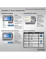
The Toshiba T200/T200CS Pen Computer uses extensive Large Scale Integration (LSI), and
Complementary Metal-Oxide Semiconductor (CMOS) technology to provide minimum size
and weight, low power usage and high reliability.  These computers include the following:

Microprocessor

The T200/T200CS uses an SL Enhanced Intel 486DX2-40 microprocessor that
operates at 40 MHz and 3.3 volts.

Math co-processor

The T200/T200CS has a math co-processor stored in the i486DX2 microprocessor.

Cache memory

The T200/T200CS has an 8 KB cache memory stored in the i486DX2 microprocessor.

Disk storage

The T200/T200CS has an internal 1.8-inch IDE 80 Megabyte (MB) Hard Disk Drive
(HDD).

Memory

The T200/T200CS comes standard with 4 MB of CMOS RAM.  This includes 640
KB of conventional memory and 3,328 KB of extended memory, which can be utilized
as expanded memory compatible with Lotus/Intel/Microsoft Expanded Memory
Specifications (LIM-EMS).

Display screen

The T200 has a 9.5-inch high resolution monochrome Liquid Crystal Display (LCD)
which displays 640x480 pixels with a 16-level gray scale, and an electromagnetic
derivative tablet (transreflective).

The T200CS has a 9.5-inch high resolution Supertwist Nematic (STN) color LCD
which displays 640x480 pixels and 256 colors, and an electromagnetic derivative
tablet.

The T200/T200CS internal display controller supports Video Graphics Array (VGA)
on the internal/external display and Super VGA (SVGA) on the external display.

Batteries

The T200/T200CS has three different batteries:  a main battery, a backup battery, and
a Real Time Clock (RTC) battery.

Summary of Contents for T200

Page 1: ...e T200 T200CS comes standard with 4 MB of CMOS RAM This includes 640 KB of conventional memory and 3 328 KB of extended memory which can be utilized as expanded memory compatible with Lotus Intel Microsoft Expanded Memory Specifications LIM EMS Display screen The T200 has a 9 5 inch high resolution monochrome Liquid Crystal Display LCD which displays 640x480 pixels with a 16 level gray scale and a...

Page 2: ...o the printer through a parallel printer cable Serial port The T200 T200CS has one 9 pin serial interface port Ext keyboard port The T200 T200CS has an external keyboard interface port for connection with a PS 2 compatible keyboard Ext monitor port The T200 T200CS has an external monitor interface port for connection with an analog VGA or SVGA display 72 pin Expansion port The T200 T200CS has a 72...

Page 3: ...T200 T200CS 1 3 The T200 T200CS Pen Computer is shown in Figure 1 1 Its system configuration is shown in Figure 1 2 Figure 1 1 T200 T200CS Pen Computer Figure 1 2 T200 T200CS System Unit Configuration ...

Page 4: ...1 4 T200 T200CS 1 2 System Unit Block Diagram Figure 1 3 is a block diagram of the computer s system unit These port signals also output to the 72 pin Expansion port Figure 1 3 Block Diagram ...

Page 5: ...maining 114 bytes for system configuration data OSC X2 generates 32 768 KHz for RTC A Keyboard Controller KBC One 80C42 chip is used This KBC includes the keyboard interface controller and controls the external keyboard The following memories Standard RAM 4 MB Cache memory 8 KB inside CPU BIOS ROM 128 KB 96 KB are used This ROM contains Initial Reliability Test IRT Basic Input Output System BIOS a...

Page 6: ...ss Controller DMA Controller I O Controller Address Latch Controller 32 Bit to 16 Bit Controller Address Latch DMA Address Generator Refresh Address Generator I O Register Compatible I O Port Saving the data of the Register in resume Controller Toshiba Special Register Processing Speed Controller Data Bus Change Controller Data Latch PCMCIA Controller Gate Array This gate array has the following f...

Page 7: ...200 T200CS 1 7 SMI Controller Gate Array This gate array has the following functions Tablet Controller Tablet Microprocessor Communication Controller SMI Controller Others Contrast Adjust PWM Controller ...

Page 8: ...re 1 4 The specifications for the FDD are provided in Table 1 1 Figure 1 4 3 5 Inch FDD Table 1 1 3 5 Inch FDD Specifications Item 2 MB mode 1 MB mode Storage capacity KB Unformatted 2 000 1 000 Formatted 1 474 737 Number of heads 2 2 Number of cylinders 80 80 Access time ms Track to track 3 3 Average 181 181 Head settling time 15 15 Recording track density tpi 135 135 Data transfer rate Kbps 500 ...

Page 9: ...igure 1 5 Specifications for the HDD are provided in Table 1 2 Figure 1 5 1 8 Inch HDD Table 1 2 1 8 Inch HDD Specifications Item 80 MB ZA1094 Storage capacity MB Formatted 85 0 Number of disks 2 Data heads 3 Data surfaces 3 Tracks per surface 2 750 Sectors per track 20 Bytes per sector 512 Access time ms Track to track 8 Average 18 Maximum 35 Rotation speed rpm 3 571 Data transfer rate bps To fro...

Page 10: ... LCD receives vertical and horizontal synchronizing signals 8 bit data signals 4 bit upper block data signal and 4 bit lower block data signal and shift clock for data transmission All signals are CMOS level compatible The sidelit LCD is shown in Figure 1 6 and its specifications are provided in Table 1 3 Figure 1 6 Monochrome LCD Table 1 3 Monochrome LCD Specifications Item Specifications Number ...

Page 11: ... illuminate the LCD s FL The FL inverter board is shown in Figure 1 7 and its specifications are provided in Table 1 4 Figure 1 7 Monochrome LCD FL Inverter Board Table 1 4 Monochrome LCD FL Inverter Board Specifications Item Specifications Input Voltage VDC 5 Power W 2 7 Output Voltage VAC 1 100 r m s Current mA 5 5 r m s Frequency KHz 39 ...

Page 12: ...ives vertical and horizontal synchronizing signals 16 bit data signal 8 bit upper block data signal 8 bit lower block data signal display enable signal and shift clock for data transmission All signals are CMOS level compatible The STN LCD is shown in Figure 1 8 The LCD specifications are provided in Table 1 5 Figure 1 8 STN Color LCD Table 1 5 STN Color LCD Specifications Item Specifications Numb...

Page 13: ...e LCD s Fluorescent Lamp The FL inverter board is shown in Figure 1 9 and its specifications are described in Table 1 6 Figure 1 9 STN Color LCD FL Inverter Board Table 1 6 STN Color LCD FL Inverter Board Specifications Item Specifications Input Voltage VDC 5 Power W 4 Output Voltage VAC 1 100 r m s Current mA 6 0 r m s Frequency KHz 47 ...

Page 14: ...re shown in Figures 1 10 and 1 11 and their specifications are provided in Table 1 7 Figure 1 10 T200 Tablet Figure 1 11 T200CS Tablet Table 1 7 Tablet Specifications Item Specifications Material Electromagnetic derivative Voltage VDC 5V Current mA 30 In use 23 In suspend 5 2 In sleep Resolution mm 0 1 Precision mm 0 4 Data transfer point sec 205 ...

Page 15: ...ols the LED icon and speaker 4 Turns the battery charging system on and off and detects a fully charged battery 5 Determines if the power can be turned on and off 6 Provides more accurate detection of a low battery 7 Calculates the remaining battery capacity The power supply output rating is specified in Table 1 8 Table 1 8 Power Supply Output Rating DC Regulation Maximum Use for Name voltage tole...

Page 16: ...y pack Lithium Ion 10 8 V 3 000 mAH Backup battery Nickel Metal Hydride 3 6 V 120 mAH RTC battery Lithium Vanadium 3 0 V 50 mAH 1 9 1 Main Battery The removable main battery pack is the primary power source when the AC adapter is not attached The main battery recharges the backup battery when system power is on The backup and main battery maintain the state of the computer system when AutoResume i...

Page 17: ...ttached Green The battery is fully charged An AC adapter is attached No light The AC adapter is disconnected from the computer or is connected but cannot charge the battery for one of the following reasons The battery is extremely hot Allow the computer and the battery to reach room temperature before attempting to charge the battery The battery is almost fully discharged and will not begin chargi...

Page 18: ...when the system is powered off and trickle charge when powered on Table 1 10 gives quick charging time requirements Table 1 10 Time Required For Quick Charges Charge Charging time Quick charge About 3 hours power off Quick charge About 8 hours power on If one of the following occurs the battery quick charge process stops 1 The battery becomes fully charged 2 The AC adapter or battery is removed 3 ...

Page 19: ...ackup Battery Charging Data Preservation Time Time Charging Time Power On 10 H Power Off 10 H with AC Adapter or main battery Power Off Doesn t charge Without AC Adapter and main battery Data preservation period full charge 8 H 1 9 4 RTC Battery The RTC battery provides power to keep the current date time and other setup information in memory while the computer is turned off Table 1 12 shows the c...

Page 20: ...used to enter information into the computer by writing directly onto the screen You can write letters or numerals to enter data draw gestures to enter commands or tap to select from menus The stylus is shown in Figure 1 13 Figure 1 13 The Stylus ...

Page 21: ...ions are described in Chapter 3 and detailed replacement procedures are given in Chapter 4 The following tools are necessary for troubleshooting 1 T200 T200CS Diagnostics Disk 2 Phillips head screwdriver 2 mm 3 2DD or 2HD formatted work disk for FDD testing 4 Printer port LED 5 RS 232 C wraparound connector 6 Printer wraparound connector 7 Multimeter 8 Parallel cable standard equipment 9 External ...

Page 22: ...ugh the flowchart steps verify the following Ask the user if a password is registered and if it is ask him or her to enter the pass word If the user has forgotten the password connect the printer port wraparound board F31PRT then turn the POWER switch on The computer will skip the pass word function Make sure all optional equipment is disconnected ...

Page 23: ...T200 T200CS 2 3 Figure 2 1 Troubleshooting Flowchart 1 2 ...

Page 24: ...2 4 T200 T200CS Figure 2 1 Troubleshooting Flowchart 2 2 ...

Page 25: ...play test ASYNC test printer test or real timer test perform the system board troubleshooting proce dures in Section 2 4 2 If an error is detected on the keyboard test perform the keyboard troubleshooting procedures in Section 2 7 3 If an error is detected on the floppy disk test perform the floppy disk drive troubleshooting procedures in Section 2 5 4 If an error is detected on the hard disk test...

Page 26: ...tions and components To determine if the power supply is functioning properly start with Procedure 1 and continue as instructed The proce dures described in this section are Procedure 1 Power LED Indicator Check Procedure 2 Battery LED Indicator Check Procedure 3 PCB Replacement Check ...

Page 27: ...normal or the power supply is not functioning properly go to Check 2 If any of the above indicator conditions are abnormal make sure the Power LED indicator lights are not burned out before performing the following checks Check 1 Make sure the correct AC adapter cable is firmly plugged into the Power socket on the back of the computer Check 2 If the Power LED flashes orange when the AC adapter is ...

Page 28: ...ake sure the AC adapter cable and AC cord are firmly plugged into the Power socket and wall outlet If connected correctly go to Check 2 Check 2 Make sure the battery pack is installed correctly Go to Check 3 if it is Check 3 Remove the battery pack and check that the battery terminal is clean and not bent If the terminal appears dirty clean gently with a cotton swab dipped in alcohol If the termin...

Page 29: ...he computer following the steps described in Chapter 4 Replacement Procedures then perform the following checks Check 1 Replace the upper system board with a new one and restart the system If the problem still exists go to Check 2 Check 2 Replace the lower system board with a new one and restart the system If the problem persists other FRUs may be damaged ...

Page 30: ...r not functioning properly Start with Procedure 1 and continue as instructed The procedures provided are Procedure 1 Message Check Procedure 2 Printer Port LED Check on Boot Mode Procedure 3 Printer Port LED Check on Resume Mode Procedure 4 Diagnostic Test Program Execution Check Procedure 5 Connection and Replacement Check ...

Page 31: ...TC battery If any other error message is displayed perform Check 2 a Error in CMOS Bad HDD type Check system Then tap any point on the screen with the stylus or press F1 key b Error in CMOS Bad battery Check system Then tap any point on the screen with the stylus or press F1 key c Error in CMOS Bad check sum Check system Then tap any point on the screen with the stylus or press F1 key d Error in C...

Page 32: ...ection 2 6 If error message 23 or 24 is displayed go to the FDD Troubleshooting Procedures in Section 2 5 1 CPU ERROR 2 SYSTEM ROM CHECK SUM ERROR 3 PIT ERROR 4 MEMORY REFRESH ERROR 5 TIMER OUT ERROR 6 FIRST 64KB MEMORY ERROR 7 FIRST 64KB MEMORY PARITY ERROR 8 VRAM ERROR 9 KBC ERROR 10 SYSTEM MEMORY ERROR 11 SYSTEM MEMORY PARITY ERROR 12 EXTENDED MEMORY ERROR 13 EXTENDED MEMORY PARITY ERROR 14 DMA...

Page 33: ...o the PRT port 4 Plug the printer port LED into the computer s parallel cable 5 Connect the external keyboard to the KB port 6 Hold down the space bar and turn on the computer s power 7 Read the LED status from left to right 8 Convert the status from binary to hexadecimal notation 9 If final LED status is FFh normal status go to Procedure 3 10 If final LED status matches any of the test status val...

Page 34: ...pt vector initialization 18H PIC initialization 1FH Display initialization CRTC ERROR VRAM ERROR READ DATA XXXXXXXXH WRITE DATA XXXXXXXXH 25H System memory test SYSTEM MEMORY ERROR ADDRESS XXXXXXXXH READ DATA XXXXXXXXH WRITE DATA XXXXXXXXH SYSTEM MEMORY PARITY ERROR ADDRESS XXXX0000H XXXXFFFFH 30H Error Extended memory test EXTENDED MEMORY ERROR 33H Normal ADDRESS XXXXXXXXH READ DATA XXXXXXXXH WRI...

Page 35: ...RUPT ERROR RTC UPDATE ERROR A0H NDP initialization A6H Expansion I O ROM C0H Boot password2 checks for no access right FEH Pre boot setup FFH Expansion system ROM NOTES These error codes are not displayed on hot boot mode This error code is not displayed on cold boot mode Check 1 If any of the following error codes are displayed go to Procedure 5 01h 02h 03h 04h 05h 06h 07h 08h 09h 0Ah 0Bh 0Ch 0Dh...

Page 36: ...Convert the status from binary to hexadecimal notation 9 If final LED status is FFh normal status go to Procedure 3 10 If final LED status matches any of the test status values in Table 2 2 perform Check 1 Table 2 2 Printer Port LED Resume Mode Error Status Error status Meaning of status 00H RAM BIOS error F0H Press the reset switch F1H Suspend process error The system will suspend while FDD is ac...

Page 37: ...sts from the Diagnostic Test Menu Refer to Chapter 3 Tests and Diagnostics for more information on how to perform the tests 1 System test 2 Memory test 3 Printer test 4 ASYNC test 5 Real Timer test 6 PCMCIA test 7 Tablet test 8 NDP test If an error is detected during the tests go to Procedure 5 ...

Page 38: ...ode detects any of the following codes go to Check 1 00H F0H F1H F2H F6H FAH FDH If the IRT test Resume mode detects any of the following codes go to Check 2 F4H F5H F7H F8H F9H FBH FEH If any of the following diagnostic tests detects an error go to Check 1 System test NDP test Printer test Async test PCMCIA test If any of the following diagnostic tests detects an error go to Check 2 Memory test R...

Page 39: ...st Program Execution Check Procedure 1 Functioning External FDD Check Connect a functioning external 3 5 inch FDD to the computer s FDD port Check the FDD operation If the FDD is operating properly the user s FDD is malfunctioning If the FDD does not operate properly go to Procedure 2 Procedure 2 FDD Connection Check Make sure the external 3 5 inch FDD cable is firmly connected to the FDD port If ...

Page 40: ...DD diagnostics test is executing go to Check 1 Table 2 3 Floppy Disk Drive Error Code and Status Code Status 01h Bad command 02h Address mark not found 03h Write protected 04h Record not found 06h Media removed 08h DMA overrun error 09h DMA boundary error 10h CRC error 20h FDC error 40h Seek error 60h FDD not drive error 80h Time out error EEh Write buffer error FFh Data compare error Check 1 If t...

Page 41: ...he computer then perform the follow ing checks Check 1 Type C and press Enter Go to Check 2 if the drive will not change to C Go to Procedure 2 if the drive changes to C Check 2 Type FDISK and press Enter Choose Display Partition Information from the FDISK menu If drive C is listed go to Check 3 If drive C is not listed return to the FDISK menu and choose the option to create a DOS partition on dr...

Page 42: ...rm Procedure 3 If the following messages do not appear perform Check 3 Insert system disk in drive Press any key when ready or Non System disk or disk error Replace and press any key Check 3 Using the Toshiba MS DOS system disk install a system program on the hard disk using the SYS command If the following message appears on the display the system program has been transferred to the HDD Restart t...

Page 43: ...rs on the display the HDD is formatted Format complete If any other error message appears on the display refer to the Toshiba MS DOS Manual for more information and perform Check 2 Check 2 Using the T200 T200CS Diagnostic Disk format the HDD with a low level format option Refer to Chapter 3 Tests and Diagnostics for more information about the diagnostic program If the following message appears on ...

Page 44: ...and Status Code Status 01h Bad command 02h Address mark not found 04h Record not found 05h HDC not reset error 07h Drive not initialized 08h HDC overrun DRQ 09h DMA boundary error 0Ah Bad sector 0Bh Bad track error 10h ECC error 11h ECC recover enable 20h HDC error 40h Seek error 80h Time out error AAh Drive not ready BBh Undefined error CCh Write fault E0h Status error EEh Access time out error F...

Page 45: ... keyboard is malfunctioning If the keyboard is not functioning properly go to Procedure 2 Procedure 2 External Keyboard Connection Check Make sure the external keyboard cable is firmly connected to the KB port If this cable is disconnected or loose connect it to the KB port If the external keyboard still does not function properly go to Procedure 3 Procedure 3 Diagnostic Test Program Execution Che...

Page 46: ...yed Abnormal lines are displayed Some pixels do not light If the backlight lights but no characters are displayed Go to Procedure 4 Any other problem Go to Procedure 3 Procedure 1 Brightness and Contrast Control Check Change the brightness and contrast by tapping the adjust point of the display with the stylus If the brightness and contrast do not change go to Procedure 4 Procedure 2 External CRT ...

Page 47: ...he T200 T200CS Diagnostic Disk This program checks the display controller on the system board After loading Toshiba MS DOS run the Diagnostic Program Refer to Chapter 3 Tests and Diagnostics for details If an error is detected go to Procedure 4 If an error is not detected the display is function ing properly ...

Page 48: ...display unit and check the cable connections shown in Figures 2 3 and 2 4 Refer to Chapter 4 Replacement Procedures for more information about how to disassemble the computer If any of these cables is not connected firmly re connect it and repeat Procedures 1 2 and 3 If the problem still exists perform Procedure 5 Figure 2 3 T200 Display Connection Figure 2 4 T200CS Display Connection ...

Page 49: ...ome screen functions do not operate properly perform Check 1 Check 1 Replace the display module and test the display again If the problem persists perform Check 2 Check 2 Replace the FL inverter board and test the display again If the problem persists perform Check 3 Check 3 Replace the display cable and test the display again If the problem persists perform Check 4 Check 4 The upper system board ...

Page 50: ... the system board by a cable This cable may be disconnected or damaged Disassemble the computer as described in Chapter 4 Replacement Procedures and perform the following checks Check 1 Make sure the tablet cable is not damaged and is connected to the lower system board If this cable is damaged replace it with a new one If the cable is discon nected firmly re connect it Perform Procedure 1 again I...

Page 51: ...D TEST DISPLAY TEST FLOPPY DISK TEST PRINTER TEST ASYNC TEST HARD DISK TEST REAL TIMER TEST PCMCIA TEST TABLET TEST NDP TEST The following equipment is needed to perform some test programs T200 T200CS Diagnostics Disk all tests Optional external 3 5 inch FDD Formatted working disk for the floppy disk drive test Cleaning kit to clean floppy disk drive heads Head Cleaning Printer wraparound connecto...

Page 52: ...parallel cable Printer Test PCMCIA wraparound connector PCMCIA Test and printer wraparound connector Printer Test to each port 3 Insert the Diagnostic disk and turn on the computer 4 A cross hair cursor will appear Tap the cursor or press Enter The following menu will appear Select items Enter Specify Esc Exit NOTES To use the stylus tap the appropriate number or command in the menu at right Up Aw...

Page 53: ...n 99 exits the submenus of the Diagnostic Test and returns to the DIAGNOSTICS MENU TOSHIBA Personal Computer XXXXX DIAGNOSTICS Version 1 XX C Copyright TOSHIBA Corp 19XX DIAGNOSTICS TEST MENU 1 SYSTEM TEST 2 MEMORY FORMAT 3 KEYBOARD TEST 4 DISPLAY TEST 5 FLOPPY DISK TEST 6 PRINTER TEST 7 ASYNC TEST 8 HARD DISK TEST 9 REAL TIMER TEST 10 PCMCIA TEST 11 TABLET TEST 12 NDP TEST 88 ERROR RETRY COUNT SE...

Page 54: ...ear SYSTEM TEST TTSSDSS SUB TEST XX PASS COUNT XXXXX ERROR COUNT XXXXX WRITE DATA XX READ DATA XX ADDRESS XXXXX STATUS XXX error status name SUB TEST MENU 01 ROM checksumum 02 HW status 03 Version check 99 Exit to DIAGNOSTIC TEST MENU Select items Enter Specify Esc Exit Break Break 0 A 1 B 2 C 3 D 4 E 5 F 6 7 Up Aw 8 Dn Aw 9 R Aw R L Aw BS Esc Enter Enter ...

Page 55: ...st program when an error is found and displays the operation guide on the right side of the display screen as shown below ERROR STATUS NAME HALT OPERATION 1 Test end 2 Continue 3 Retry These three selections have the following functions 1 Terminates the test program and exits to the subtest menu 2 Continues the test 3 Restarts the test from the beginning Selecting NO keeps the test running even if...

Page 56: ...ule 06 Backup memory 07 Cache memory 3 KEYBOARD 01 Pressed key code display 4 DISPLAY 01 VRAM read write 02 Character attributes 03 Character set 04 80x25 30 Character display 05 320x200 Graphics display 06 640x200 Graphics display 07 640x350 400 480 Graphics display 08 Display page 09 H pattern display Border color 10 DAC pallet 11 VGA color graphics display 5 FDD 01 Sequential read 02 Sequential...

Page 57: ...al read 02 Address uniqueness 03 Random address data 04 Cross talk peak shift 05 Write read compare CE 06 Write specified address 07 Read specified address 08 ECC circuit 09 Sequential write 10 W R C specified address 9 REAL TIMER 01 Real time 02 Backup memory 03 Real time carry 10 PCMCIA 01 I O card test PCMCIA 11 TABLET 01 TABLET ADJUST 02 9POINT test 03 CURSOR MOVING test 04 WRITE DOT test 12 N...

Page 58: ... reads and displays hardware status as shown below 76543210 H W status 10001000 Bit7 Bit6 CPU clock 40MHz Bit5 Notch signal 2HD Bit4 FDD type 2MB Bit3 Bit2 Drive A B Ext B Bit1 External FDD OFF Bit0 Internal FDD 2HD Table 3 2 lists hardware bit status for each bit tested Press Enter to return to the Subtest Menu Table 3 2 Hardware Bit Status Bit H W status 1 0 7 Reserved 6 CPU clock speed 20 MHz 4...

Page 59: ...s to test program reference data When the read information is lower than the reference data the speaker sounds and the following screen image is displayed Press the S key to exit The display is unchanged if the read information is higher ROM BIOS V1 00 OK V1 10 ROM BOOT V1 00 OK V1 00 KBC Version V1 26 NG V1 00 PS Micom Version V1 35 OK V1 35 Reference data Current data ...

Page 60: ...ed by the exclusive ORing XORing to the address segment and address offset in conventional memory program end to 640 KB then reads the new data and compares the result with original data Subtest 03 RAM refresh real mode This subtest writes a 256 byte unit of constant data to conventional memory 0 to 640 KB then reads the new data and compares the result with original data Constant data is AAAAh an...

Page 61: ...6 MB Select the number corresponding to the installed memory card Subtest 06 Backup Memory This subtest writes constant data to memory from address C8000h to CFFFFh then reads new data and compares the result with original data Constant data is 0000h 5555h AAAAh and FFFFh Subtest 07 Cache memory To test cache memory a pass through write read comparison of 5A data is run repeatedly to a test area 7...

Page 62: ...splay When a key is pressed the scan code character code and key top name are displayed on the screen in the format shown below The Ins Caps Lock Num Lock Scroll Lock Alt Ctrl Left Shift and Right Shift keys are displayed in reverse screen mode when pressed Scan codes character codes and key top names are shown in Appendix E KEYBOARD TEST IN PROGRESS 301000 Scan code Character code Keytop Ins Lock...

Page 63: ... compared to original data Subtest 02 Character Attributes mode 1 13h This subtest displays four character attribute modes normal intensified reverse and blinking The character attribute modes display foreground and intensified color 16 colors or 16 level gray scale using black blue red magenta green cyan yellow and white from the color display The following display appears when the subtest is exe...

Page 64: ...tertogglesbetweenthetwodisplays ToexittotheDISPLAYTESTmenu pressCtrl Break Subtest03 CharacterSet Inthissubtest thecharacterset address00htoFFh isdisplayedinthe40x25 charactermodeasshownbelow PRESS Enter KEY ToexittotheDISPLAYTESTmenu pressCtrl Break BLACK BLUE GREEN CYAN RED MAGENTA BROWN WHITE GRAY LIGHT BLUE LIGHT GREEN LIGHT CYAN LIGHT RED LIGHT MAGENTA YELLOW INTENSE WHITE ...

Page 65: ...NOPQRSTUVWXYZ _ abcdefghijklmnopqrstuvw 0123456789 ABCDEFGHIJKLMNOPQRSTUVWXYZ _ abcdefghijklmnopqrstuvwx 0123456789 ABCDEFGHIJKLMNOPQRSTUVWXYZ _ abcdefghijklmnopqrstuvwxy 0123456789 ABCDEFGHIJKLMNOPQRSTUVWXYZ _ abcdefghijklmnopqrstuvwxyz 0123456789 ABCDEFGHIJKLMNOPQRSTUVWXYZ _ abcdefghijklmnopqrstuvwxyz 0123456789 ABCDEFGHIJKLMNOPQRSTUVWXYZ _ abcdefghijklmnopqrstuvwxyz 0123456789 ABCDEFGHIJKLMNOPQ...

Page 66: ... DRIVEN DRIVEN PRESS ENTER KEY ToexittotheDISPLAYTESTmenu pressCtrl Break Subtest07 640x350 400 480GraphicsDisplay mode10 74 12 Thissubtestdisplayseven odd andalldotsin640x350 640x400and640x480 dotgraphicsmode10 74 12asshownbelow 640 XXX GRAPHICS DISPLAY EVEN DOTS ODD DOTS ALL DOTS DRIVEN DRIVEN DRIVEN PRESS ENTER KEY PressEntertochangedisplayedimagesize ToexittotheDISPLAYTEST menu press Ctrl Brea...

Page 67: ...HHH HHHHHHHHHHHHHHHHHHHHHHHHHHHHHHHHHHHHHHHHHHHHHHHHHH HHHHHHHHHHHHHHHHHHHHHHHHHHHHHHHHHHHHHHHHHHHHHHHHHH HHHHHHHHHHHHHHHHHHHHHHHHHHHHHHHHHHHHHHHHHHHHHHHHHH HHHHHHHHHHHHHHHHHHHHHHHHHHHHHHHHHHHHHHHHHHHHHHHHHH HHHHHHHHHHHHHHHHHHHHHHHHHHHHHHHHHHHHHHHHHHHHHHHHHH HHHHHHHHHHHHHHHHHHHHHHHHHHHHHHHHHHHHHHHHHHHHHHHHHH HHHHHHHHHHHHHHHHHHHHHHHHHHHHHHHHHHHHHHHHHHHHHHHHHH HHHHHHHHHHHHHHHHHHHHHHHHHHHHHHHHHHHHHHH...

Page 68: ...or latch test 1 256 times 2 endless To exit press Ctrl Break Then press Enter Subtest11 VGAcolorgraphicsdisplay Thissubtestdisplayseightscreens Thefirstscreenshowsmanycolors mode13 at once The next three display 64 shades mode 13 of red green and blue successively Next asinglescreendisplaysmanycolors mode5F Thelastthree display256shadesofred greenandblue Press Enter to change the display Press Ctr...

Page 69: ...FDD 1 FDD 2 FDD1 2 2 Select the media type of the floppy disk to be tested and tap or press Enter Media in drive X mode 2DD 2D 2D 2HD 2HD 3 Select the track to start the test on and tap or pressEnter Tappingorpressing Enter alonesetsthestarttracktozero Test start track Enter 0 dd 00 79 4 Thefloppydisktestmenuwillappearafterthestarttracknumberisselected Selecta subtestnumberandtaporpressEnter Thefo...

Page 70: ...equentialRead Write ThissubtestcontinuouslywritesdatapatternB5ADADhtoallthespecifiedtracks selectedinsubtest01 Dataisthenreadandcomparedtotheoriginaldata Subtest03 RandomAddress Data Thissubtestwritesrandomdatatorandomaddressesonalltracksdefinedin subtest01 Dataisthenreadandcomparedtotheoriginaldata Subtest04 WriteSpecifiedAddress Thissubtestwritesspecifieddatatoaspecifiedtrack head andaddress Whe...

Page 71: ... subtest Subtest 01 Ripple Pattern This subtest prints characters for codes 20h through 7Eh line by line while shifting one character to the left at the beginning of each new line 0123456789 ABCDEFGHIJKLMNOPQRSTUVWXYZ _ abcdefghijklmno 0123456789 ABCDEFGHIJKLMNOPQRSTUVWXYZ _ abcdefghijklmnop 0123456789 ABCDEFGHIJKLMNOPQRSTUVWXYZ _ abcdefghijklmnopq 0123456789 ABCDEFGHIJKLMNOPQRSTUVWXYZ _ abcdefghi...

Page 72: ... THIS LINE SHOWS COMPRESSED PRINT 4 THIS LINE SHOWS EMPHASIZED PRINT 5 THIS LINE SHOWS DOUBLE STRIKE PRINT 6 ALL CHARACTERS PRINT 0123456789 ABCDEFGHIJKLMNOPQRSTUVWXYZ _ abcdefghijklmn opqrstuvwxyz Subtest 03 Wraparound NOTE To execute this subtest a printer wraparound connector with a parallel cable must be connected to the computer printer port The printer wraparound connector 34M741986G01 wirin...

Page 73: ...Channel 3 XXXXh Select the Channel number 1 2 3 The serial I O port address is specified by the XXXXh number Select the serial port channel number and press Enter to start the subtest Subtest 01 Wraparound board NOTE An RS 232C wraparound connector 34M741621G01 must be connected to the RS 232C port by a parallel cable to execute this subtest The wraparound connector wiring diagram is shown in Appe...

Page 74: ... diagram for the RS 232C direct cable is shown in Appendix F This subtest sends 20h through 7Eh data to the receive side then receives the sent data and compares it to the original data Subtest 04 Point to point Receive This subtest is used with subtest 03 This subtest receives data from the send side then sends the received data Subtest 05 Interrupt Test This subtest checks the Interrupt Request ...

Page 75: ... 2 Select the HDD number to be tested and tap or press Enter The following mes sage will appear HDC F W error retry YES NO 3 This message is used to select the retry operation when the hard disk controller detects an error Select 1 or 2 and tap or press Enter The following message will appear Data compare error dump NO YES 4 This message is used to select the error dump operation when a data compa...

Page 76: ...ritten to each sector is then read and compared with the original data There are three ways the HDD can be read Forward sequential Reverse sequential Random Subtest 03 Random Address Data This subtest writes random data to random addresses on the HDD cylinder head and sector This data is then read and compared to the original data Subtest 04 Cross Talk Peak Shift This subtest writes eight types of...

Page 77: ...d HDD cylinder and head Subtest 08 ECC circuit This subtest checks the Error Check and Correction ECC circuit functions of a specified HDD cylinder and head Subtest 09 Sequential write This subtest writes specified 2 byte data to all HDD cylinders Subtest 10 W R C specified address This subtest writes data to a specified HDD cylinder and head then reads the data and compares it to the original dat...

Page 78: ...RESS ENTER KEY TO EXIT TEST 2 If the current date is not correct input the correct date at the Enter new date prompt and press Enter The following prompt will appear Enter new time 3 If the current time is not correct input the correct time in 24 hour format Pressing Enter toggles between the time and date To exit press Ctrl Break Subtest 02 Backup Memory This subtest performs the following backup...

Page 79: ... are erased This subtest checks real time clock increments verifying the date and time are displayed in the following format Current date 12 31 1992 Current time 23 59 58 Pressing Enter displays the following Current date 01 01 1993 Current time 00 00 00 PRESS Enter KEY TO EXIT TEST Press Ctrl Break to exit ...

Page 80: ...CIA slot Address line REG CE 1 CE 2 line Data line Speaker line Wait line BSY BVD1 line This subtest is executed in the following order Sub Address Good Bad Contents 01 00001 nn xx Address line 00001 nn xx REG CE 1 CE 2 nn A0 90 80 00 02 00002 ww rr Data line ww write data rr read data 03 00003 Speaker line 04 00004 40 80 xx Wait line 40 xx 80 05 00005 nn xx Other lines BSY BVD1 nn 21 00 ...

Page 81: ...or Tap the cursor at the center to complete the test Subtest 02 9 POINT test This test checks the screen matrix addresses Nine cross hair cursors appear Tap each cursor If the tapped position corresponds to the cursor coordinate the cursor disappears When all cursors are cleared the test is over Subtest 03 CURSOR MOVING test This test checks the address and the stylus s switch A cross hair cursor ...

Page 82: ...3 32 T200 T200CS ...

Page 83: ...from the DIAGNOSTIC TEST MENU and tap or press Enter The NDP test contains one subtest that tests the computer s NDP functions Subtest 01 NDP This test checks the following functions of NDP Control word Status word Bus Addition Multiplication Press Ctrl Break to exit ...

Page 84: ...board 02 IPS Interface Error 03 Interface Error 04 Retransmit Error FDD 01 Bad Command 02 Address Mark Not Found 03 Write Protected 04 Record Not Found 06 Media Removed 08 DMA Overrun Error 09 DMA Boundary Error 10 CRC Error 20 FDC Error 40 Seek Error 60 FDD Not Drive Error 80 Time Out Error EE Write Buffer Error Printer 01 Time Out 08 Fault 10 Select Line 20 Out Of Paper 40 Power Off 80 Busy Line...

Page 85: ... Error 10 ECC Error 11 ECC Recover Enable 20 HDC Error 40 Seek Error 80 Time Out Error AA Drive Not Ready BB Undefined Error CC Write Fault E0 Status Error EE Access Time Out Error NDP 01 No CO PROCESSOR 02 Control Word Error 03 Status Word Error 04 Bus Error 05 Addition Error 06 Multiply Error PCMCIA C1 Address Line Error C2 REG Line Error C3 CE 1 Line Error C4 CE 2 Line Error C5 Data Line Error ...

Page 86: ...scribed in Tables 3 4 and 3 5 respectively Table 3 4 Hard Disk Controller Status Register Contents Bit Name Description 7 BSY 0 HDC is busy Busy 1 HDC is ready 6 DRDY 0 Hard disk drive is not ready to accept any command Drive ready 1 Hard disk drive is ready 5 DWF 0 DWF error is not detected Drive write fault 1 Write fault condition occurred 4 DSC 0 The hard disk drive heads are not settled over a...

Page 87: ...ta error has been detected 5 Not used 4 IDNF 0 Other Identification 1 There was no ID field in the requested sector 3 Not used 2 ABRT 0 Other Abort 1 Illegal command error or a drive status error occurred 1 TK00 0 The hard disk found track 0 during a recalibrate command Track 0 1 The hard disk could not find track 0 during a recalibrate command 0 Not used ...

Page 88: ...ting transfer hard disk contents onto a floppy disk s 3 18 1 Function Description 1 All track FORMAT This option performs a low level format of all hard disk tracks as listed in Table 3 6 below NOTE Before executing the All Track FORMAT option check for bad tracks using the Bad Track CHECK option or display a list of bad tracks on the HDD Table 3 6 Hard Disk Formatting Sequence 80 MB Items ZA1094 ...

Page 89: ... tracks is displayed when the program is complete If an error other than a bad track is detected the program is terminated 3 18 2 Operations CAUTION After the hard disk is formatted set the partition Refer to the customer s operating system documentation for details on partitioning the disk Select 2 from the DIAGNOSTIC MENU and tap or press Enter to display the following menu DIAGNOSTICS HARD DISK...

Page 90: ...3 40 T200 T200CS Head XX Sector XX Model name ...

Page 91: ...l Track Format as described in Item d below WARNING Current DISK data will be completely destroyed Press Bad cylinder number dddd key Press Bad head number dd key Enter the cylinder and head number in the format above in decimal notation Repeat for each bad track to format After entering the bad tracks tap or press Enter to execute the format d All Track Format All tracks are formatted as good tra...

Page 92: ... a bad track enter the drive interleave cylinder and head numbers as indicated in the screen prompts shown below Drive number select 1 1 2 2 Interleave number 1 1 8 Press Cylinder number dddd Press Head number dd Tap or press Enter to return to the Hard Disk Format menu 4 Bad track CHECK This subtest reads the entire disk and displays a bad track list The test is termi nated in case of a bad track...

Page 93: ...the DIAGNOSTIC MENU and tap or press Enter to display the following messages DIAGNOSTICS FLOPPY DISK HEAD CLEANING VX XX Mount cleaning disk s on drive s Press any key when ready 2 Remove the Diagnostics Disk from the FDD insert the cleaning disk and tap or press Enter 3 When the cleaning start message appears the FDD head cleaning has begun 4 The display returns to the DIAGNOSTIC MENU when the pr...

Page 94: ...DD or memory address ADDR 7 Write data WD 8 Read data RD 9 HDC status HSTS 10 Error status name ERROR STATUS NAME 3 20 2 Operations 1 Select 5 in the DIAGNOSTIC MENU and tap or press Enter to log error infor mation into RAM or to a floppy disk Error information is displayed in the following format XXXXX ERRORS CNT TS NAME PASS STS ADDR WD RD HSTS STATUS NAME 001 FDD 02 0000 103 00001 00 00 FDD WRI...

Page 95: ...y to the previous page 3 returns to the Diagnostic Menu 4 erases all error log information in RAM 5 outputs the error log information to a printer 6 reads log information from a floppy disk 7 writes log information to a floppy disk 3 In the case of error retry OK a capital R will be placed at the beginning of the error status but not added to the error count ...

Page 96: ...ble density 48 67 5 TPI MFM mode 512 bytes 9 sectors track b 2DD Double sided double density double track 96 135 TPI MFM mode 512 bytes 9 sectors track c 2HD Double sided high density double track 96 135 TPI MFM mode 512 bytes 18 sectors track 2 COPY This program copies data from a source floppy disk to a target floppy disk 3 DUMP This program displays floppy disk both 3 5 inch and 5 25 inch conte...

Page 97: ...nsert the work disk and tap Enter or press any key The following message will be displayed when the FDD format is executed FDD TYPE TRACK XXX FDD TYPE HEAD X FDD TYPE SECTOR XX Format start track head XXX X After the floppy disk is formatted the following message will appear Format complete Another format 1 Yes 2 No e Type 1 to display the message from step c above Type 2 to return to the DIAGNOST...

Page 98: ...message from step b is displayed again After the floppy disk has been copied the following message will appear Copy complete Another copy 1 Yes 2 No e To copy another disk type 1 and the message from step a will be displayed again Enter 2 to return to the DIAGNOSTIC MENU 4 DUMP program a Select dump to display the following message DIAGNOSTICS HARD DISK FLOPPY DISK DUMP VX XX Drive type select 1 F...

Page 99: ...3 49 e Insert a source disk and press any key and the following message will appear Max address Track 0079 Head 01 Sector 09 Track number f Set a track number to dump The system will access the disk and dump a list ...

Page 100: ...f printer ports 9 Extended Memory Size 10 PS Micom Version 11 Math Co processor 3 23 2 Operations Select 8 from the DIAGNOSTIC MENU and tap or press Enter to display the system con figuration menu SYSTEM CONFIGURATION BIOS ROM VERSION VX XX BOOT ROM VERSION VX XX KBC VERSION VX XX 639KB MEMORY 1 FLOPPY DISK DRIVE S 1 ASYNC ADAPTER 1 HARD DISK DRIVE S 1 PRINTER ADAPTER XXXXXKB EXTENDED MEMORY PS MI...

Page 101: ...Mode c LCD Gray Scale Level T200 only d Power On Display 3 COM PCMCIA PRT a Serial Port b PC Card Slot 1 c PC Card Slot 2 d Printer Port Type 4 Hard Disk 5 Battery a Battery Save Mode b Remaining Capacity 6 Password 7 Others a Power up Mode b CPU Cache c Processing Speed d Speaker Volume e Alarm Power On f Boot Priority 8 Battery Save Options a CPU Sleep Mode b Display Auto Off c HDD Auto Off d Sy...

Page 102: ... following message is displayed Are you sure Y N The changes you made will cause the system to re boot Thesystemre boots COM PCMCIA PRT Serial Port COM1 IRQ4 3F8H PC Card Slot 1 PCMCIA PC Card Slot 2 PCMCIA Printer Port Type Output Total 4096 KB Base 640 KB Extended 3328 KB Shadow BIOS ROM 128 KB MEMORY BIOS version x xx T200 SETUP Display Adapter VGA compatible LCD Display Mode Color LCD Gray Sca...

Page 103: ... functionally related groups This section describes each group and its options 1 Memory This group lists values for computer memory a Total This field displays the total amount of memory installed and is calculated by the computer These values may not be changed by the user b Base This field displays the amount of base conventional memory 640 KB and is calculated by the computer These values may n...

Page 104: ...twareisdisplayedbest inmonochromemode NOTE The LCD Display Mode is automatically set to conform to the CRT being used and cannot be changed c LCD Gray Scale Level T200 only Use this option which appears in SETUP to switch between normal and reverse video on the T200 It does not appear on the T200CS The options are Normal 16 levels Displaysblacktextonawhitebackgroundwith16shades of gray Reverse 16 ...

Page 105: ...lot 1 Use this option to select PC Card slot usage PCMCIA Choose this selection when a PCMCIA card is installed This isthe default Others ChoosethisselectionwhenaToshibacardmodem isinstalled NOTE Only one PC Card Slot can be set to Others For example if PC Card Slot 1 is set to Others and you also set PC Card Slot 2 to Others PC Card Slot 1 automatically changes to PCMCIA When Others is chosen use...

Page 106: ... or COM2 default Use the Power option to turn the power to the modem on or off When the PC Card Slot 1 option is set to Others the Power option is dis played in the sub window The Power option indicates the setting in CMOS d Printer Port Type This option sets the communication mode for the printer port to either output only or bi directional For most printers the port should be set to Output With ...

Page 107: ...mi bright NOTE The System Auto Off message does not appear in boot mode User Setting Use this option to set battery save parameters on the sub window BATTERY SAVE OPTIONS If selected the automatic setting feature Long Life or Normal Life is disabled and the user preferred parameters become effec tive The default setting in the sub windows depends on the Battery Save Mode Full Power or Low Power Fo...

Page 108: ... these options depends primarily on the kind of software or peripherals used a Power up Mode Use this option to choose between AutoResume and boot mode Boot Turns on boot mode This is the default Resume TurnsontheAutoResumefeature b CPU Cache Use this feature to enable or disable the CPU cache Enabled Enables the CPU cache This is the default Disabled DisablesCPUcache c Processing Speed Thisfeatur...

Page 109: ...wer On Use this option to set the time for the system to turn on automatically This option can be set to expected transmission times for periods of personal absence The option does not automatically turn off the system 00 00 00 Sets the power on time 24 hour clock Disabled Disablesthealarm f Boot Priority This option selects disk drive priority for boot up FDD HDD Thecomputerlooksforbootablefilesf...

Page 110: ... to disable or set the duration of the HDD automatic power off function Disabled DisablesHDDautomaticpower off xx Min AutomaticallyturnsoffpowertotheHDDifitisnotused for the duration set Duration xx can be set to 3 5 10 15 20or30minutes d System Auto Off Use this option to enable or disable the system automatic off function when power upmodeissettoResume InBootmode thisfeatureisalwaysdisabled andt...

Page 111: ...gineachprocedurebyremovingtheAC adapterandthebatterypackasinstructedinsection4 2 TheBatteryPack 1 Donotdisassemblethecomputerunlessitisoperatingabnormally 2 Useonlythecorrectandapprovedtools 3 Makesuretheworkingenvironmentisfreefromthefollowingelementswhetherusingor storingthecomputer Dust and contaminates Static electricity Extreme heat cold and humidity 4 Make sure the FRU you are replacing is c...

Page 112: ...hesides oftheconnector Gentlypullonthecabletomakesurethecableissecure Ifyoupulloutthe connector connectitagainmakingsuretheconnector spressureplateisfullyliftedwhenyouinsert thecable Standard pin connectors are used with all other cables These connectors can be connected and disconnected by simply pulling them apart or pushing them together Assembly Procedures Thecomputermustbere assembledafterdis...

Page 113: ...e of your repairs and lower the cost for damaged or destroyed parts The following equipment is neces sary to disassemble and reassemble the computer OneM2Phillips headscrewdrivertoremoveandreplaceM1andM2screws Tweezers toliftoutscrewsthatyoucannotgraspwithyourfingers ESDmatsforthefloorandthetableyouareworkingon AnESDwriststraporheelgrounder Anti staticcarpetingorflooring Airionizersinhighlystatics...

Page 114: ... 2 Turn the computer upside down 3 Slideopenthecovertothebatterylatchandpressthereleasebuttonuntilitclicks Thebatterywillpopoutslightly Figure4 1 4 Thereisasecondsafetylatchthatholdsthebatterypackafterthereleasebuttonis pressed To clear the second latch insert your fingers in the gap between the computerandthebatterypackandpushcarefullywithonehanduntilthebattery packisfree Figure4 1 5 Firmlygraspt...

Page 115: ...e battery pack is designed to fit into the computer in only one way To install the computer s battery pack follow the steps below and refer to Figure 4 1 1 Gentlyslidethebatterypackintothebatteryslot 2 Pushthebatterypackinuntilitlocksintoplace Figure4 1 ...

Page 116: ...wer cord and all external cables connected to the computer 2 Removethebatterypackasdescribedinsection4 2 3 Open the expansion slot cover 4 Grasptheplastictabandpullitsothecardcomespartiallyoutofthecomputer Figure 4 2 5 Graspthecardandpullitoutofthecomputer Figure4 2 Figure 4 2 Removing the Optional Memory Card CAUTION DO NOT touch the connecting edge of the memory card Debris or oil in or on the c...

Page 117: ...nalmemorycardismarkedwiththeword insert andanarrow pointingtowardtheconnectingedge Turnthememorycardsothatitisfacingupand carefullyinserttheconnectingedge arrowfirst intotheslot Pushgentlytoensurea firmconnection Figure4 2 2 Close the expansion slot cover 3 Install the battery pack as described in section 4 2 The computer automatically configures all additional memory ...

Page 118: ...scribed in section 4 2 3 Open the expansion slot cover 4 PresstheejectbuttonoftheoptionalPCMCIAcardslot1andtheoptionalPCMCIA cardwillpoppartiallyout Figure4 3 5 Graspthecardandpullitoutofthecomputer Figure4 3 6 PresstheejectbuttonoftheoptionalPCMCIAcardslot2andtheoptionalPCMCIA cardwillpoppartiallyout Figure4 3 7 Graspthecardandpullitoutofthecomputer Figure4 3 Figure 4 3 Removing the Optional PCMC...

Page 119: ...the card is almost fully seated you will feel some resistance Press gently untiltheejectbuttonpopsout Donotforcethecardintoposition 3 To install a PCMCIA card into PCMCIA card slot 2 carefully insert the card making sure the card is right side up and the contact surface is inserted first Fig ure 4 3 4 When the card is almost fully seated you will feel some resistance Press gently untiltheejectbutt...

Page 120: ...l cables connected to the computer 2 Remove the battery pack optional memory card and optional PCMCIA cards as described in sections 4 2 4 3 and 4 4 3 Remove the one M2 5x6 screw from the HDD cover Figure 4 4 Figure 4 4 Removing the HDD Cover NOTE The HDD cover is held in place by one screw and two latches Be careful to rotate the cover out as indicated in Figure 4 4 when removing it and engage th...

Page 121: ...etheHDDcoveroutofitsseatingandgentlydisconnecttheRTC battery fromtheHDDcover Figure4 5 Figure 4 5 Disconnecting the RTC Battery 5 LiftupandpullontheHDDhandletodisconnecttheHDDconnector Figure4 6 Figure 4 6 Removing the HDD with Bracket ...

Page 122: ...4 12 T200 T200CS 6 Removethefourflat headM1 6x4silverscrewssecuringthebrackettotheHDD andslipoffthebracket Figure4 7 Figure 4 7 Removing the HDD ...

Page 123: ... 6x4 silver screws Figure 4 7 2 Place the HDDon the HDD slot Make sure theHDDconnector connects to the systemboardPJ408correctlyasshowninFigure4 6 3 Connect the RTCbattery to the HDDcover Figure 4 5 4 Replace the HDD cover and secure it with the one M2 5x6 screw Figure 4 4 5 Install the optional PCMCIA card optional memory card and battery pack as described in sections 4 2 4 3 and 4 4 ...

Page 124: ...n sections 4 2 4 3 4 4 and 4 5 3 Remove the four M2 5x30 screws and one M2 5x10 screw Figure 4 8 NOTES 1 The terminals for the battery extend outside the back cover so be careful not to damage them when removing the cover 2 The latches tightly secure the back cover To release them firmly press on the back cover above each latch as you pry it free 3 When removing the cover you will need to press in...

Page 125: ...8 Be sure to carefully fit the cover over the battery terminal 2 Makesuretheguidetubesarealignedandseated thensecurethefourM2 5x30 screws and M2 5x10 screw Figure 4 8 3 Install the HDD optional PCMCIA card optional memory card and battery pack as described in sections 4 2 4 3 4 4 and 4 5 NOTE When installing the cover you will need to press in the eject button of the optional PCMCIA card 2 ...

Page 126: ...f the power to the computer Disconnect the AC adapter power cord and all external cables connected to the computer 2 Remove the battery pack optional memory card optional PCMCIA cards HDD and back cover as described in sections 4 2 4 3 4 4 4 5 and 4 6 3 Peelbacktheprotectivetapeandreflecttheinsulatoraway thendisconnectthe backupbatterycablefromPJ203 andliftoutthebackupbattery Figure4 9 4 Reflectth...

Page 127: ...e the six brass M2 5x4 screws securing the upper system board Figure 4 10 7 CarefullyrotatetheuppersystemboardoutofitsseatinganddisconnecttheFLin verterboardcablefromPJ204 Figure4 10 Figure 4 10 Removing the Upper System Board ...

Page 128: ...oardtoconnectthem NOTE Make sure the upper system board is not attached to the lower system board components Refer to Figure 4 11 Figure 4 11 Installing the Upper System Board 4 Secure the six M2 5x4 screws on the upper system board Figure 4 10 5 Reflecttheinsulatoraway thenconnecttheRTCbatterycabletoPJ403 Figure4 9 6 ConnectthebackupbatterycabletoPJ203 Figure4 9 andreplacetheprotective tape 7 Con...

Page 129: ...nnect the AC adapter power cord and all external cables connected to the computer 2 Remove the battery pack optional memory card optional PCMCIA cards HDD back cover upper system board backup battery and RTC battery as described in sections 4 2 4 3 4 4 4 5 4 6 and 4 7 3 Removetheinsulator thenremovethethreeM2 5x4screwssecuringthelower systemboard Figure4 12 Figure 4 12 Removing the T200 Lower Syst...

Page 130: ...20 T200 T200CS 4 Carefullyrotatethelowersystemboardoutofitsseatinganddisconnectthetablet cable fromPJ407andthedisplay cablefromPJ404 Figure4 13 Figure 4 13 Disconnecting the Tablet Cable and Display Cable ...

Page 131: ...nectthedisplaycableto PJ404andcarefullyrotatethesystemboard Figure4 13 3 Placethelowersystemboardonthebaseframe Figure4 12 4 Secure the three M2 5x4 screws on the lower system board Figure 4 12 then replacetheinsulator 5 Installtheuppersystemboard backupbattery RTCbattery backcover HDD optionalPCMCIAcard optionalmemorycard andbatterypackasdescribedin sections 4 2 4 3 4 4 4 5 4 6 and 4 7 ...

Page 132: ...all external cables connected to the computer 2 Remove the battery pack optional memory card optional PCMCIA cards HDD back cover upper system board backup battery and RTC battery as described in sections 4 2 4 3 4 4 4 5 4 6 and 4 7 3 Removetheblackinsulator thendisconnectthedisplaycablefromPJ405 Figure4 14 4 Peelbackthewhitetape thenremovethethreeM2 5x4screwssecuringthelower systemboard Figure4 1...

Page 133: ...T200 T200CS 4 23 5 Carefullyrotatethelowersystemboardoutofitsseatinganddisconnectthetablet cablefromPJ407 Figure4 15 Figure 4 15 Disconnecting the Tablet Cable ...

Page 134: ...otatethelowersystemboard Figure4 15 2 Connectthedisplaycableto PJ405 Figure4 14 andreplacetheblackinsulator overthedisplaycable 3 Placethelowersystemboardonthebaseframe Figure4 14 4 Secure the three M2 5x4 screws on the lower system board Figure 4 14 5 Install the upper system board backup battery RTC battery back cover HDD optional PCMCIA card optional memory card and battery pack as described in...

Page 135: ...les connected to the computer 2 Remove the battery pack optional memory card optional PCMCIA cards HDD back cover upper system board backup battery and RTC battery as described in sections 4 2 4 3 4 4 4 5 4 6 and 4 7 3 Removethetape anddisconnecttheFL inverter cablefromCN1andtheFLcable fromCN2 Figure4 16 4 RemovethethreeM2 5x4screwssecuringtheFLinverterboardandliftouttheFL inverterboard Figure4 16...

Page 136: ...rter board T200 FL inverter board P000196850 T200 CS FL inverter board P000195520 1 Connect the FL inverter cable to CN1 on the FL inverter board and the FLcable to CN2 Figure4 16 2 ReplacetheFLinverterboardandsecureitwiththethreeM2 5x4screws Figure 4 16 3 Installthelowersystemboard uppersystemboard backupbattery RTCbattery backcover HDD optionalPCMCIAcard optionalmemorycard andbatterypackas descr...

Page 137: ...ndrefertoFigures4 17through4 19 1 Turnoffthepowertothecomputer DisconnecttheACadapter powercordandall externalcablesconnectedtothecomputer 2 Remove the battery pack optional memory card optional PCMCIA cards HDD back cover upper system board backup battery RTC battery lower system board and FL inverter board as described in sections 4 2 4 3 4 4 4 5 4 6 4 7 4 8 and 4 10 3 RemovethetwoM2 5x4screwsse...

Page 138: ...4 28 T200 T200CS 5 Removethetabletcover Figure4 18 Figure 4 18 Removing the T200 Tablet Cover 6 Removethetablet Figure4 19 Figure 4 19 Removing the T200 Tablet ...

Page 139: ...lesateachcornerwiththecorre spondingpostsontheLCDmodule 2 Placethemiddleframeonthedisplaymoduleandmakesurethatthecablingis covered thensnapthefourlatchesintoplace Figure4 17 3 Securethemiddleframewiththetwo2 5x4screws Figure4 17 4 InstalltheFLinverterboard lowersystemboard uppersystemboard backupbattery RTCbattery backcover HDD optionalPCMCIAcard optionalmemorycard and battery pack as described in...

Page 140: ...sbelowandrefertoFigures4 20through4 22 1 Turnoffthepowertothecomputer DisconnecttheACadapter powercordandall externalcablesconnectedtothecomputer 2 Removethebatterypack optionalmemorycard optionalPCMCIAcards HDD backcover uppersystemboard backupbattery RTCbattery lowersystemboard and FL inverter board as described in sections 4 2 4 3 4 4 4 5 4 6 4 7 4 8 4 9 and 4 10 3 RemovethetwoM2 5x4screwssecur...

Page 141: ... 5 Liftupthedisplaycableandliftthetabletcoveroutofthedisplaymodule Figure4 21 Figure 4 21 Removing the T200CS Tablet Cover Figure 4 22 Removing the T200CS Tablet 6 Liftthetabletoffthetwoguidepostsandremoveit Figure4 22 ...

Page 142: ...ftthecablesupandoutoftheway thenplacethetabletcoveronthetablet Figure 4 21 3 Placethemiddleframeonthedisplaymodule makingsurethecablingiscovered then snapthefourlatchesintoplace Figure4 20 4 SecurethemiddleframewiththetwoM2 5x4screws Figure4 20 5 InstalltheFLinverterboard lowersystemboard uppersystemboard backupbattery RTCbattery backcover HDD optionalPCMCIAcard optionalmemorycard and battery pack...

Page 143: ... inverter board and tablet as described in sections 4 2 4 3 4 4 4 5 4 6 4 7 4 8 4 10 and 4 11 3 Removethedisplaymodulefromthedisplaymask Figure4 23 Figure 4 23 Removing the T200 Display Module Installing the T200 Display Module ToinstalltheT200 sdisplaymodule followthestepsbelowandrefertoFigure4 23 1 Placethedisplaymoduleonthedisplaymask Figure4 23 2 Installthetablet FLinverterboard lowersystemboa...

Page 144: ...TCbattery lowersystemboard FL inverter board and tablet as described in sections 4 2 4 3 4 4 4 5 4 6 4 7 4 8 4 10 and 4 11 3 Disconnectthedisplaycablefromthedisplaymodule Installing the T200CS Display Module ToinstalltheT200CS sdisplaymodule followthestepsbelow 1 Connectthedisplaycabletothedisplaymodule 2 Installthetablet FLinverterboard lowersystemboard uppersystemboard backup battery RTCbattery ...

Page 145: ...3 CarefullyliftouttheFLunitfromthedisplaymodule 4 RemovethetwoM2x2 5flatscrewssecuringtheFLcover Figure4 24 5 UnlatchthefourlatchestoremovetheFL Figure 4 24 Removing the T200 FL Installing the T200 FL ToinstalltheT200 sFL followthestepsbelowandrefertoFigure4 24 1 SnapinthefourlatchesoftheFLcovertotheFLunit 2 Secure the FL cover with two M2x2 5 flat screws Figure 4 24 3 PlacetheFLunitontheLCDpanel ...

Page 146: ...movethebatterypack optionalmemorycard optionalPCMCIAcards HDD backcover uppersystemboard backupbattery RTCbattery lowersystemboard FLinverterboard andtabletasdescribedinsections4 2through4 7 4 9 4 10and 4 12 3 RemovethefourM2 5x4screwssecuringtheFLunitandLCDpaneltotheLCD cover Figure4 25 Figure 4 25 Removing the Four Screws 4 Removethesix M2x2 flat screwssecuringtheFL unit cover Figure 4 26 Figure...

Page 147: ... T200CS FL Installing the T200CS FL ToinstalltheT200CS sFL followthestepsbelowandrefertoFigures4 25through4 27 1 Place the FL on the FLunit and cover the FL using a reflective sheet Figure 4 27 2 Secure the reflective sheet with tape 3 Place the FL unit cover and secure it with six M2x2 flat screws Figure 4 26 4 SecuretheFLunitwithfourM2 5x4screws Figure4 25 5 Installthetablet FLinverterboard lowe...

Page 148: ...ed itmaybenecessarytochangetheplastictip To removethetip followthestepbelowandrefertoFigure4 28 1 Removethetipandpullitout Usethetweezers Figure 4 28 Removing the Tip Installing the Tip Toinstallthestylus stip followthestepbelowandrefertoFigure4 28 1 Insertthenewtipandpushgentlytofullyseatit ...

Page 149: ...When installing the LCD module in the LCD cover be sure to seat it so that it is properly aligned and maximum visibility of the display is maintained 2 Carefully align the holes at the four corners of the LCD module with correspond ing holes in the cover before securing with screws Do not force the module into place stress can affect its performance The polarized surface of the panel scars easily ...

Page 150: ...ipe again Ifthesurfaceisverydirty werecommendaCRTcleaningagent Applytheagenttoa clothandthenwipethesurface Donotapplycleanserdirectlytothepanel 4 Water or other liquids left on the surface for a long period can change the screen tintorstainthescreen Besuretoquicklywipeoffanyliquid 5 DodroporstriketheLCDmodulewithahardobject glassusedinthepanelcould break or crack ...

Page 151: ...ticdis chargedamagetotheCMOS LSIcircuits 7 Do not expose the module to direct sunlight or strong ultraviolet rays for long periods 8 Do not store the module at temperatures below specifications Cold can cause liquid crystals to freeze lose their elasticity or otherwise suffer damage ...

Page 152: ...inChapter4 Disassembly beyondtheinstructionsinthismanualcancausemalfunctions 10 If transporting the module do not use packing materials that contain epoxy resin amine or silicon glue alcohol or oxime These materials can release gas that can damage panel polarization ...

Page 153: ...T200 T200CS B 1 Appendix B Board Layout B 1 Upper System Board FOGSD2 Figure B 1 Upper System Board FOGSD2 Front ...

Page 154: ...B 2 T200 T200CS Figure B 2 Upper System Board FOGSD2 Back ...

Page 155: ... display connector J PJ7 72 pinExpansionconnector K PJ8 PCMCIA slot 2 connector L PJ9 PCMCIA slot 1 connector M PJ201 DC IN connector N PJ202 Main battery connector O PJ204 FL inverter connector Table B 2 Upper ICs and Connectors on the System Board Back Mark Number Name A IC1 CPU486DX2 B IC2 System controller gate array C IC3 Clockgenerator D IC4 Superintegration T9901 E IC5 BIOS ROM F IC7 KBC G ...

Page 156: ...B 4 T200 T200CS B 2 Lower System Board FOGSU2 Figure B 3 Lower System Board FOGSU2 Front ...

Page 157: ...T200 T200CS B 5 Figure B 4 Lower System Board FOGSU2 Back ...

Page 158: ...1 to IC408 System memory B IC412 RTC C PJ401 Joint connector D PJ403 RTCbatteryconnector E PJ405 T200CSdisplayconnector F PJ408 HDDconnector Table B 4 Lower ICs and Connectors on the System Board Back Mark Number Name A PJ402 Memory card connector B PJ404 T200 display connector C PJ407 Tabletconnector ...

Page 159: ...010 O 16 MA08 110 O 56 CAS1 010 O 17 MA09 110 O 57 CAS2 010 O 18 MA10 110 O 58 CAS3 010 O 19 D00 110 I O 59 MWE1 010 O 20 D01 110 I O 60 MWE2 010 O 21 D02 110 I O 61 GND 22 D03 110 I O 62 SD00 100 I O 23 D04 110 I O 63 SD01 100 I O 24 D05 110 I O 64 SD02 100 I O 25 D06 110 I O 65 SD03 100 I O 26 D07 110 I O 66 SD04 100 I O 27 D08 110 I O 67 SD05 100 I O 28 D09 110 I O 68 SD06 100 I O 29 D10 110 I ...

Page 160: ...GND 119 MLCLK 110 O 90 SIN 100 I 120 CLCLK 110 O 91 SOUT 100 O 121 GND 92 CTS2 000 I 122 FLTEN 000 O 93 GND 123 PNEL0 100 O 94 RTCSBY 000 O 124 CNTBEN 000 O 95 RTCWR 000 O 125 CNTRST 000 O 96 RTCAS 100 O 126 TF0 100 O 97 RTCDS 000 O 127 TF1 100 O 98 IRQ8 000 I 128 TF2 100 O 99 C32KHZ 000 O 129 TLCH 100 O 100 GND 130 VCC 101 LD0 110 O 131 VCC 102 LD1 110 O 132 VCC 103 LD2 110 O 133 VCC 104 LD3 110 ...

Page 161: ...110 I O 22 GND 10 ACK 000 I 23 GND 11 BUSY 100 I 24 GND 12 PE 100 I 25 GND 13 SELCT 100 O C 3 PJ3 FDD Connector 26 Pin Table C 3 FDD Connector Pin Assignment 26 Pin Pin Signal I O Pin Signal I O 01 FVCC201 14 IFSTEP 010 O 02 IFINOX 000 I 15 GND 03 FVCC201 16 IFWDAT 010 O 04 FVCC201 O 17 GND 05 FVCC201 18 IFWEN 010 O 06 DSKCHG 000 I 19 GND 07 IFDASL 010 20 IFTRKO 000 I 08 IFRADY 000 I 21 GND 09 IFH...

Page 162: ...5 PS 2 Keyboard Connector 6 Pin Table C 5 PS 2 Keyboard Connector Pin Assignment 6 Pin Pin Signal I O Pin Signal I O 01 EKBDAT I O 04 VCC 02 N C 05 EKBCLK I O 03 GND 06 N C C 6 PJ6 External Display Connector 15 Pin Table C 6 External Display Connector Pin Assignment 15 Pin Pin Signal I O Pin Signal I O 01 ARED 110 O 09 N C 02 AGREEN 110 O 10 GND 03 ABLUE 110 O 11 N C 04 N C 12 N C 05 GND 13 CHSYNC...

Page 163: ...O 47 IFLOD2 000 12 IFLD01 000 O 48 GND 13 IFAMON 000 O 49 GND 14 MOUSCK 120 I O 50 GND 15 RKBCLK 100 I O 51 RTS1 110 O 16 CTS1 110 I 52 VCC 17 DSR1 110 I 53 DCINP I 18 DCINP I 54 DCINP I 19 DCINP I 55 DCINP I 20 DCINP I 56 GND 21 RXD1 010 I 57 TXD1 010 O 22 DTR1 110 O 58 RI1 110 I 23 DCD1 110 I 59 MOUSDT 100 I O 24 GND 60 GND 25 RKBDAT 100 I O 61 PRCHEK 000 I O 26 IFWEN 000 O 62 IHMED 000 I 27 IFR...

Page 164: ...AD08A 100 O 46 CAD17A 100 O 13 CAD13A 100 O 47 CAD18A 100 O 14 CAD14A 100 O 48 CAD19A 100 O 15 WEA 000 O 49 CAD20A 100 O 16 BSYA 000 I 50 CAD21A 100 O 17 MCVCCA 51 MCVCCA 18 MCVPP1A 52 MCVPP2A 19 CAD16A 100 O 53 CAD22A 100 O 20 CAD15A 100 O 54 CAD23A 100 O 21 CAD12A 100 O 55 CAD24A 100 O 22 CAD07A 100 O 56 CAD25A 100 O 23 CAD06A 100 O 57 N C 24 CAD05A 100 O 58 CRSETA 100 O 25 CAD04A 100 O 59 WAITA...

Page 165: ...AD08B 100 O 46 CAD17B 100 O 13 CAD13B 100 O 47 CAD18B 100 O 14 CAD14B 100 O 48 CAD19B 100 O 15 WEB 000 O 49 CAD20B 100 O 16 BSYB 000 I 50 CAD21B 100 O 17 MCVCCB 51 MCVCCB 18 MCVPP1B 52 MCVPP2B 19 CAD16B 100 O 53 CAD22B 100 O 20 CAD15B 100 O 54 CAD23B 100 O 21 CAD12B 100 O 55 CAD24B 100 O 22 CAD07B 100 O 56 CAD25B 100 O 23 CAD06B 100 O 57 N C 24 CAD05B 100 O 58 CRSETB 100 O 25 CAD04B 100 O 59 WAITB...

Page 166: ...2 DCM C 12 PJ202 Main Battery Connector 10 Pin Table C 12 Main Battery Connector Pin Assignment 10 Pin Pin Signal I O Pin Signal I O 01 06 MBRD 02 TH 07 u VSS 03 DC 08 OV 04 u VCC 09 THG 05 MBSD 10 C 13 PJ203 Backup Battery Connector 2 Pin Table C 13 Backup Battery Connector Pin Assignment 2 Pin Pin Signal I O Pin Signal I O 01 SUBBAT 02 GND C 14 PJ204 FL Inverter Connector 6 Pin Table C 14 FL Inv...

Page 167: ...A1 O 14 A2 O 58 A3 O 15 VCC5 59 A5 O 16 A4 O 60 A7 O 17 VCC3 61 A9 O 18 A6 O 62 A11 19 A8 O 63 GND 20 A10 O 64 A13 21 A12 65 RAS1 O 22 RAS0 O 66 CAS2 O 23 CAS0 O 67 GND 24 CAS1 O 68 CAS3 O 25 VCC3 69 RAS3 O 26 RAS2 70 WE O 27 VCC5 71 PD1 I O 28 PD2 I O 72 PD3 I O 29 PD4 I O 73 GND 30 PD6 I O 74 PD5 I O 31 RFU O 75 PD7 I O 32 RFU O 76 PD8 I O 33 D017 77 RFU O 34 D09 I O 78 RFU O 35 VCC3 79 D035 36 ...

Page 168: ...D3 O 18 DOFF O 07 LD2 O 19 VSS 08 LD1 O 20 CP2 O 09 LD0 O 21 VSS 10 UD3 O 22 CP1 O 11 UD2 O 23 S O 12 UD1 O C 18 PJ405 T200CS Display Connector 30 Pin Table C 18 T200CS Display Connector Pin Assignment 30 Pin Pin Signal I O Pin Signal I O 01 VEE 16 VCC 02 GND 17 VCC 03 DISP O 18 UD2 140 O 04 FPF 140 O 19 UD3 140 O 05 LPF 140 O 20 GND 06 CLCLK 140 O 21 CDU0 140 O 07 GND 22 CDU1 140 O 08 LD0 140 O 2...

Page 169: ... I O 14 TCN13 100 I O 29 TCN28 100 I O 15 TCN14 100 I O 30 TCN29 100 I O C 20 PJ408 HDD Connector 50 Pin Table C 20 HDD Connector Pin Assignment 50 Pin Pin Signal I O Pin Signal I O 01 N C 26 N C 02 N C 27 N C 03 N C 28 GND 04 N C 29 IOWR 000 O 05 N C 30 GND 06 N C 31 IORD 000 O 07 RESET 000 O 32 GND 08 GND 33 IOCRDY 100 I 09 HSD07 100 I O 34 N C 10 HSD08 100 I O 35 N C 11 HSD06 100 I O 36 GND 12 ...

Page 170: ...T200 T200CS D 1 Appendix D USA Display Codes Table D 1 USA Display Codes ...

Page 171: ...5 12 _ 0C 8C 4E F0 4E 13 0D 8D 55 F0 55 15 BkSp 0E 8E 66 F0 66 16 Tab 0F 8F 0D F0 0D 17 Q 10 90 15 F0 15 18 W 11 91 1D F0 1D 19 E 12 92 24 F0 24 20 R 13 93 2D F0 2D 21 T 14 94 2C F0 2C 22 Y 15 95 35 F0 35 23 U 16 96 3C F0 3C 2 24 I 17 97 43 F0 43 2 25 O 13 98 44 F0 44 2 26 P 19 99 4D F0 4D 2 27 1A 9A 54 F0 54 28 1B 9B 5B F0 5B 29 42 2B AB 5D F0 5D 5 30 Caps Lock 3A BA 58 F0 58 31 A 1E 9E 1C F0 1C ...

Page 172: ...33 B3 41 F0 41 2 54 34 B4 49 F0 49 2 55 35 B5 4A F0 4A 2 57 Shift R 36 B6 59 F0 59 58 Ctrl 1D 9D 14 F0 14 3 60 Alt L 38 B8 11 F0 11 3 61 Space 39 B9 29 F0 29 62 ALT R E0 38 E0 B8 E0 11 E0 F0 11 75 Ins E0 52 E0 D2 E0 70 E0 F0 70 1 76 Del E0 53 E0 D3 E0 71 E0 F0 71 1 79 E0 4B E0 CB E0 6B E0 F0 6B 1 80 Home E0 47 E0 C7 E0 6C E0 F0 6C 1 81 End E0 4F E0 CF E0 69 E0 F0 69 1 83 E0 48 E0 C8 E0 75 E0 F0 75...

Page 173: ...119 F8 42 C2 0A F0 0A 120 F9 43 C3 01 F0 01 121 F10 44 C4 09 F0 09 122 F11 57 D7 78 F0 78 3 123 F12 58 D8 07 F0 07 3 124 PrintSc 6 6 6 6 6 126 Pause 7 7 7 7 7 202 Fn 4 Notes 1 Scan codes differ by mode 2 Scan codes differ by overlay function 3 Combination with Fn key makes different codes 4 Fn key does not generate a code by itself 5 This key corresponds to key No 42 in 102 key model 6 Refer to Ta...

Page 174: ...able E 2 shows scan codes with the left Shift key In combination with the right Shift key scan codes are changed as listed below With left Shift With right Shift Set 1 E0 AA E0 B6 E0 2A E0 36 Set 2 E0 F0 12 E0 F0 59 E0 12 E0 59 Table E 3 Scan Codes in Numlock Mode Cap Key Code set 1 Code set 2 No top Make Break Make Break 75 INS E0 2A E0 52 E0 02 E0 AA E0 12 E0 70 E0 F0 70 E0 F0 12 76 DEL E0 2A E0...

Page 175: ...F0 6C 09 8 8 48 C8 75 F0 75 10 9 9 49 C9 7D F0 7D 11 0 37 B7 7C F0 7C 23 U 4 4B CB 6B F0 6B 24 I 5 4C CC 73 F0 73 25 O 6 4D CD 74 F0 74 26 P 4A CA 7B F0 7B 37 J 1 4F CF 69 F0 69 38 K 2 50 D0 72 F0 72 39 L 3 51 D1 7A F0 7A 40 4E CE 79 F0 79 52 M 0 52 D2 70 F0 70 53 33 B3 41 F0 41 54 53 D3 71 F0 71 55 E0 35 E0 B5 40 4A E0 F0 4A Table E 6 Scan Codes with Ctrl Key Key Code set 1 Code set 2 top Shift M...

Page 176: ... T200CS Table E 7 Scan Codes with Alt Key Key Code set 1 Code set 2 top Shift Make Make Pause Common E1 ID 45 E1 SD C5 E1 14 77 E1 F0 14 F0 77 Ctrl E0 46 E0 C6 E0 7E E0 F0 7E This key generates only make codes ...

Page 177: ... PD0 11 BUSY Figure F 1 Printer Wraparound Connector F 2 RS 232C Wraparound Connector 3 TD 2 RD 7 RTS 8 CTS 1 CD 4 DTR 6 DSR 9 RI Figure F 2 RS 232C Wraparound Connector F 3 RS 232C Direct Cable 9 Pin to 9 Pin 3 TD 2 RD 4 DTR 6 DSR 8 CTS 9 RI 7 RTS 1 CD 5 GND 5 GND 2 RD 3 TD 1 CD 7 RTS 6 DSR 4 DTR 8 CTS 9 RI Figure F 3 RS 232C Direct Cable 9 pin to 9 pin T200 T200CS F 1 ...

Page 178: ...2 T200 T200CS F 4 RS 232C Direct Cable 9 Pin to 25 Pin 1 CD 4 RTS 2 RD 2 TD 3 TD 3 RD 4 DTR 5 CTS 6 DSR 22 RI 5 GND 7 GND 7 RTS 8 CD 6 DSR 20 DTR 8 CTS 9 RI Figure F 4 RS 232C Direct Cable 9 pin to 25 pin ...

Page 179: ...tethepassword thefollowingtoolsarerequired Aprinterwraparoundconnector Aparallelcable standardequipment Deleting the Password 1 SetthesystemtoBootMode 2 Turnoffthepowertothecomputer 3 ConnecttheparallelcabletothePRTport 4 Connecttheprinterwraparoundconnectortotheparallelcable 5 Turnonthepowertothecomputer WhentheOSisloaded thepasswordisautomati callyremoved 6 Removetheprinterwraparoundconnectorand...

Page 180: ...es below to perform the BIOS rewrite program 1 SetthesystemtoBootMode 2 Turnoffthepowertothecomputer 3 RemoveanyexternalcablesandPCMCIAcard 4 Connecttheexternal3 5 inchFDDandexternalkeyboardtothecomputer 5 InserttheBIOSrewritediskintotheFDD 6 Turnonthepowertothecomputer 7 ChecktheBIOSversionmessagewhenitisdisplayed IftheBIOSversioniscorrect pressY 8 WhentheBIOSre writingisfinishedandthesystemspeak...

Reviews: