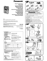
Toshiba SD-V280, Service Manual
The Toshiba SD-V280 is a versatile entertainment system that combines a DVD player and VHS recorder into one compact device. Enhance your home theater experience with this all-in-one unit. To make the most out of its features, ensure to download the free Owner's Manual from manualshive.com, where you can find a comprehensive guide.
Share
Download


Reviews:
No comments
Related manuals for SD-V280
130
Brand: Tascam Pages: 2
700
Brand: Nakamichi Pages: 16
CR-2
Brand: Nakamichi Pages: 36
CR-2
Brand: Nakamichi Pages: 9
322
Brand: Tascam Pages: 5
6155
Brand: NAD Pages: 3
616
Brand: NAD Pages: 2
616
Brand: NAD Pages: 58
RQ-SW88V
Brand: Panasonic Pages: 2
RQ-CR18V
Brand: Panasonic Pages: 4
RQ-2102 - Cassette Recorder
Brand: Panasonic Pages: 7
RQ-SX47
Brand: Panasonic Pages: 4
RQ-SX53
Brand: Panasonic Pages: 3
RQ-SX47
Brand: Panasonic Pages: 2
RQ-CR15V
Brand: Panasonic Pages: 3
RQ-SX43
Brand: Panasonic Pages: 3
RQ-SX76
Brand: Panasonic Pages: 4
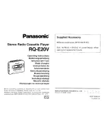
RQE20V - PERSONAL STEREO-LOW
Brand: Panasonic Pages: 10


