background image

CORDLESS TELEPHONE

PUBLISHED IN JAPAN, Nov., 1999

SERVICE MANUAL

FILE NO.  2B0-9909

FD-4809

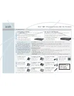
Summary of Contents for FD-4809

Page 1: ...CORDLESS TELEPHONE PUBLISHED IN JAPAN Nov 1999 SERVICE MANUAL FILE NO 2B0 9909 FD 4809 ...

Page 2: ... circuitry etc may alter the safety characteristics of these models and potentially create a hazardous situation for the user Any design alterations or additions will void the manufacturer s warranty and will further relieve the manufacturer of responsibility for personal injury or property damage resulting therefrom 2 PRODUCT SAFETY NOTICE Many electrical and mechanical parts in this chassis have...

Page 3: ...Modular Jack Cradle Base Antenna IN USE CHARGE LED PAGE Button Charging Contact VOL RING Button Antenna SELECT Button CID Caller ID Button Dialpad Dot matrix display Date Caller ID indication example Time Caller s telephone number Caller s name Number of calls Battery compartment 900MHz CALLER ID FD 4809 OPERATING CONTROLS HANDSET CONTROLS AND FUNCTIONS BASE UNIT CONTROLS AND FUNCTIONS LCD ...

Page 4: ...elease the PAGE key when entering TEST mode 1 with IN USE CHARGE LED lighting Alignment Procedure Alignment Point Location on Base Main PCB and Base RF PCB Power Meter RF Test Point J3 DC IN 9V Jack AC 120V 60Hz BASE Unit AC Adapter step 1 Adjustment VR202 TX Power Remarks Connect the Power Meter to the RF test point on the Base MAIN PCB Adjust VR202 for a 4 0dBm reading on the Power Meter VR202 B...

Page 5: ...D lighting Alignment Procedure step 1 Preset to SG 1mV No modulation Remarks Press the PAGE key for 3 times to enter the TEST Mode 4 Connect the RF Signal Generator to the RF test point on the Base MAIN PCB Make sure that the frequency is 903 417756 MHz Connect the DC Voltmeter to the Discriminator test point Adjust L1 to indicate DC 0 90 V Adjustment L1 Discriminator Voltage RF Test Point AF Term...

Page 6: ...ly On while pressing and keys and keep pressing the keys continuously for approximate 2 seconds d Release keys when entering TEST mode 1 with beep Alignment Procedure VR502 RF Test Point step 1 Adjustment VR502 TX Power Remarks Connect the RF power Meter to the RF test point on the handset MAIN PCB Adjust VR502 for a 4 0dBm reading on the Power Meter RF PCB Handset PCB Power Meter RF Test Point J6...

Page 7: ...g TEST mode 1 with beep Alignment Procedure step 1 Preset to SG 1mV No modulation Remarks Press the 4 key to enter the TEST Mode 4 Connect the RF Singal Generator to the RF test point on the handset MAIN PCB Make sure that the frequency is 926 495220 MHz Connect the DC Voltmeter to the Discriminator test point Adjust L603 to indicate DC 0 90 V Adjustment L603 Discriminator Voltage RF PCB RF Test P...

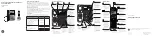
Page 8: ...7 BLOCK DIAGRAMS Base Unit ...

Page 9: ...8 Handset ...

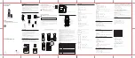
Page 10: ...9 10 SCHEMATIC DIAGRAMS Base Unit ...

Page 11: ...11 12 Handset ...

Page 12: ...l does not ring page does not ring OK OK NG NG OK NG Deletion of the Caller ID memory To delete the Caller ID memory in the EEPROM proceed with the following process 1 Connect the battery with pressing and buttons and keep pressing the buttons continuously for approximate 2 seconds 2 Release buttons when entering TEST mode with beep 3 Press CID button 4 A confirmation beep will sound after about 8...

Page 13: ...E SW of the base is pressed does pin63 of IC4 change from high to low Check IC4 and its peripheral circuit When the key of the handset is pressed can the pulse output at pin 2 of IC606 be seen Check RINGER Y601 Check R105 and S1 See 3 The base and handset cannot be connected Check IC606 OK OK OK NG OK NG NG NG At the Q609 collector can the pulse wave be seen OK Check R667 and Q609 NG ...

Page 14: ...ess PAGE key 2 times 903 417756 MHz 30kHz 30kHz Dev 1mV output signal from RF jack is applied Can the IN USE CHARGE LED be lighted OK NG Check whether there is a 30kHz waveform at C3 NG OK Check whether there is a 30kHz pulse waveform at pin 34 of IC2 Check R4 R5 R6 R8 C3 C4 C5 D1 IC2 and their peripheral circuit NG OK Check IC1 and its peripheral circuit OK Check whether the handset is able to se...

Page 15: ...RF jack is applied Check whether the bell ring NG Check whether there is the 30kHz waveform at C605 NG OK Check whether there is a 30kHz pulse waveform at pin 34 of IC602 Check R620 R621 R623 R625 C605 C607 C608 D611 IC602 and their peripheral circuit NG OK Check whether the voltage at pin 10 of IC601 is more than 1V Check IC601 and its peripheral circuit NG OK Check C606 IC606 and its peripheral ...

Page 16: ...heck Q9 RL1 and their peripheral circuits NG OK OK 5 Cannot make a phone call tone Can the base and handset be connected See 3 The base and handset be cannot be connected OK NG While in TALK MODE press dial key of the handset Can tone waveform from Pin 17 of IC2 is fed OK NG Can tone signal be heard from the handset speaker Check Q2 and its peripheral circuit NG OK Check the base TEL line circuit ...

Page 17: ...veform be fed Check handset RF unit NG OK Check whether there is the 1 kHz sine waveform at pin 22 of IC2 on the base unit NG OK Check whether there is the 1 kHz sine waveform at pin 17 of IC2 Check C7 R13 C10 R14 NG OK Check whether there is the 1 kHz sine waveform at the Q2 collector Check Q2 and its peripheral circuit NG OK Check whether the 1 kHz sine waveform from TEL line output is fed Check...

Page 18: ...he 1 kHz sine waveform at pin 12 of IC2 Check Q3 and its peripheral circuit NG OK OK TX output signal from the base is detected by the liner detector can the app 30kHz pulse waveform be fed Check base RF unit NG OK Check whether there is the 1 kHz sine waveform at pin 22 of IC602 on the handset unit NG OK Check whether there is the 1 kHz sine waveform at pin 17 of IC602 Check C611 R631 R629 R639 R...

Page 19: ... 4 23 0 0 0 0 24 OPEN OPEN 25 OPEN OPEN 26 OPEN OPEN 27 GND GND 28 0 0 3 0 0 0 3 0 Pulse Pulse 29 0 6 1 8 0 6 1 8 Sinewave Sinewave 30 OPEN OPEN 31 OPEN OPEN 32 OPEN OPEN 33 OPEN OPEN 34 OPEN OPEN 35 0 4 2 6 0 4 1 4 Float Float 36 1 2 1 6 1 2 1 6 Float Float IC2 37 0 0 0 0 38 3 0 3 0 39 GND GND 40 0 0 0 0 3 0 Pulse 41 0 0 0 0 42 0 0 3 0 0 0 3 0 Pulse Pulse 43 0 0 3 0 0 0 3 0 Pulse Pulse 44 0 0 3 0...

Page 20: ...N OPEN 61 OPEN OPEN 62 OPEN OPEN 63 3 0 3 0 64 OPEN OPEN 1 1 5 1 5 2 1 5 1 5 3 1 5 1 5 IC5 4 1 5 1 5 5 0 0 0 0 6 0 0 3 0 0 0 3 0 Sine wave Sine wave 7 0 3 3 0 0 3 3 0 Sine wave Unit V Unit V Ref No PIN STBY TALK NOTE Ref No PIN STBY TALK NOTE 8 GND GND 9 OPEN OPEN 10 3 0 3 0 11 3 0 3 0 12 0 0 0 0 IC5 13 0 0 0 0 14 OPEN OPEN 15 3 0 3 0 16 3 0 3 0 17 0 0 0 0 18 1 5 1 4 19 1 5 1 4 20 1 5 1 4 1 3 0 3 ...

Page 21: ... 0 0 6 1 4 Pulse 20 0 0 0 6 1 4 Pulse 21 0 0 0 0 22 0 0 0 6 1 4 Pulse 23 OPEN OPEN 24 OPEN OPEN 25 OPEN OPEN 26 OPEN OPEN 27 GND GND 28 0 0 3 2 Pulse Pulse 29 0 8 2 8 Pulse Pulse 30 OPEN OPEN 31 OPEN OPEN 32 OPEN OPEN 33 OPEN OPEN 34 OPEN OPEN 35 0 6 2 6 Float Float IC602 36 0 2 1 8 1 4 1 8 Float Float 37 0 0 3 0 3 0 Pulse Pulse 38 0 0 3 0 3 0 Pulse 39 GND GND 40 0 0 0 0 3 0 Pulse 41 0 0 0 0 42 0 ...

Page 22: ...JackOff 41 0 0 0 0 42 0 0 0 0 43 0 0 0 0 44 0 0 0 0 45 0 0 0 0 46 0 0 0 0 47 0 0 0 0 48 OPEN OPEN 49 GND GND 50 0 0 0 0 51 0 0 2 8 2 8 Pulse Vol Low Vol Low 52 0 0 0 0 Vol Low Vol Low 53 0 0 3 0 54 0 0 2 8 2 8 Pulse 55 0 0 2 8 56 2 8 3 0 3 0 Pulse 57 2 8 3 0 3 0 Pulse IC606 58 OPEN OPEN 59 0 0 0 0 2 8 Pulse 60 0 0 2 8 2 8 Pulse 61 0 0 0 0 2 8 Pulse 62 0 0 0 0 2 8 Pulse 63 0 0 0 0 2 8 Pulse B 0 0 0...

Page 23: ...33 MONI_3 32 MONI_2 31 MONI_1 30 XI 29 XO 28 DGND 27 TEST3 26 TEST2 25 TEST1 24 DTMF 23 1 2 3 4 5 6 7 8 9 10 11 AP IC2 ML7010 02GA D17 RB500V Anode Cathode P47 AD7 64 P46 AD6 63 P45 AD5 62 P44 AD4 61 P43 AD3 60 P42 AD2 59 P41 AD1 58 P40 AD0 57 P67 ASTB 56 P66 WAIT 55 P65 WR 54 P64 RD 53 17 P36 SCK31 18 P20 SI30 19 P21 SO30 20 P22 SCK30 21 P23RxD0 22 P24 TxD0 23 P25 ASCK0 24 V DD1 25 AV SS 26 P17 A...

Page 24: ...40 P16 INT6 39 P15 INT5 38 P14 INT4 37 1 P45 PPG4 2 P46 PPG5 3 P50 AN0 4 P51 AN1 5 P52 AN2 6 P53 AN3 7 P54 AN4 8 P55 AN5 9 P56 AN6 10 P57 AN7 11 AVcc 12 AVR P13 INT3 36 13 AVss P12 INT2 35 14 P60 SIN1 P11 INT1 34 15 P61 SOT1 P10 INT0 33 16 P62 SCK1 IC606 MB90562PFM 1 2 3 IC605 RH5RE32AA IC607 RH5VL28CA Cathode Anode Vcc 8 WP 7 6 SDA 5 1 A0 2 A1 SCL A2 3 4 Vss D619 RB500V Anode Cathode D616 S1ZB20 ...

Page 25: ...26 ELECTRICAL PARTS LOCATION Base Unit Main PCB ...

Page 26: ...27 Handset Main PCB ...

Page 27: ...28 WIRING DIAGRAMS Base Unit ...

Page 28: ...29 Handset ...

Page 29: ...30 EXPLODED VIEWS AND MECHANICAL PARTS LIST Base Unit 9 6 3 10 11 13 14 19 1 13 15 8 4 17 18 13 2 5 12 16 7 12 MAIN PCB ASSY RF MODULE BASE ANTENNA ...

Page 30: ... LABEL INDICATION 1 10 RC008313 GCAS442329Z LED LENS PMMA 1 11 RC008289 SSCW192005N SCREW BIND HD M2X5 NI 4 12 RC004893 SSCW802612N SCREW P TIGHT BIND HD D2 6X12 NI 4 13 RC000941 SSCW802608N SCREW P TIGHT BIND HD D2 6X8 NI 5 14 RC001752 SSCW283012N SCREW TAPPING BIND SP WASHER D3X12 NI 1 15 RC005696 RUTC457032Z WOOL COATED PAPER WOOL TACK 2 16 RC008677 PLBZ443466Z LABEL TA POLYESTER 1 17 RC008664 ...

Page 31: ...32 Handset 7 8 4 15 1 16 17 18 17 5 10 22 11 21 12 20 2 9 6 19 13 14 3 17 RF MODULE HANDSET MAIN PCB ASSY 23 ...

Page 32: ... 11 RC008367 GHDZ442430A HOLDER SPEAKER ABS 1 12 RC008464 LNBZ342420Z KEY RUBBER SI 1 13 RC008345 PLBS442900Z LABEL ID PAPER 1 14 RC008692 KDPZ443151Z PLATE DISPLAY PC 1 15 RC008289 SSCW192005N SCREW BIND HD M2X5 NI 2 16 RC003327 SSCW802610N SCREW P TIGHT BIND HD D2 6X10 NI 2 17 RC000941 SSCW802608N SCREW P TIGHT BIND HD D2 6X8 NI 8 18 RC008465 RCUN443255Z CUSHION RF MODULE NBR 1 19 RC008466 RCUN4...

Page 33: ...L 1608 0 01UF 50V K B C10 RC005214 BCMM812214Z CERAMIC M L 1608 220PF 50V J CH C11 RC005202 BCML311045Z CERAMIC M L 1608 0 1UF 16V K B C12 RC008640 BCML313935Z CERAMIC M L 1608 0 039UF 16V K B C13 RC000777 BCZY0120001 SEMI CONDUCTOR CZ 120 0 022UF 18V C14 RC001794 BCAZ111016Z ELECTROLYTIC 100UF 10V M C 156 C15 RC005204 BCML811025Z CERAMIC M L 1608 0 001UF 50V K B C16 RC008020 BCZY0260001 MYLAR MET...

Page 34: ...IC M L 1608 0 01UF 50V K B C60 RC005202 BCML311045Z CERAMIC M L 1608 0 1UF 16V K B C61 RC001802 BCAZ314706Z ELECTROLYTIC 47UF 16V M C 156 C62 RC005205 BCML811035Z CERAMIC M L 1608 0 01UF 50V K B C63 RC005205 BCML811035Z CERAMIC M L 1608 0 01UF 50V K B C65 RC005205 BCML811035Z CERAMIC M L 1608 0 01UF 50V K B C66 RC001810 BCAZ814796Z ELECTROLYTIC 4 7UF 50V M C 156 C67 RC005205 BCML811035Z CERAMIC M ...

Page 35: ...4Z CERAMIC M L 1608 150PF 50V J CH C634 RC005202 BCML311045Z CERAMIC M L 1608 0 1UF 16V K B C635 RC008296 BCSH901006Z TANTALUM CHIP 10UF 6 3V M C 122 C636 RC008296 BCSH901006Z TANTALUM CHIP 10UF 6 3V M C 122 C637 RC005203 BCML512235Z CERAMIC M L 1608 0 022UF 25V K B C638 RC005202 BCML311045Z CERAMIC M L 1608 0 1UF 16V K B C639 RC008731 BCXK311050Z CERAMIC M L 2125 1UF 16V Z F C640 RC005202 BCML311...

Page 36: ...AY0246003 1N4148 D17 RC008083 BDAY1063001 RB500V 40 D18 RC003195 BDAY0432004 ZENER HZK6C D608 RC005534 BDAY0931001 LED PG3822K D609 RC005534 BDAY0931001 LED PG3822K D610 RC005534 BDAY0931001 LED PG3822K D611 RC004630 BDAY0422001 DCC010 D613 RC001826 BDAY0433001 RLS4148 D614 RC001635 BDAY0274001 1SS226 D615 RC001635 BDAY0274001 1SS226 D616 RC004904 BDAY0792001 BRIDGE S1ZB20 4062 D617 RC008448 BDAY1...

Page 37: ...2736Z T1 RC003234 BTFY0265001 TRANSFORMER HYBRID TF 265 AT 24E7 03 TRANSISTORS Q1 RC002245 BDBC2714124 2SC2714 Y Q2 RC001637 BDBC2712303 2SC2712 GR Q3 RC003031 BDBC1623648 2SC1623 L6 Q4 RC008275 BDBA0812695 2SA812 M M6A Q5 RC003200 BDBD0471111 2SD471 L Q6 RC003200 BDBD0471111 2SD471 L Q8 RC003200 BDBD0471111 2SD471 L Q9 RC003031 BDBC1623648 2SC1623 L6 Q10 RC003031 BDBC1623648 2SC1623 L6 Q604 RC003...

Page 38: ...05240 BRFC161024Z CARBON FIXED CHIP 1K 1 16W J R29 RC005251 BRFC163304Z CARBON FIXED CHIP 33 1 16W J R30 RC005241 BRFC161034Z CARBON FIXED CHIP 10K 1 16W J R31 RC005258 BRFC164744Z CARBON FIXED CHIP 470K 1 16W J R32 RC005285 BRFC165634Z CARBON FIXED CHIP 56K 1 16W J R33 RC008765 BRFC161004Z CARBON FIXED CHIP 10 1 16W J R34 RC005256 BRFC164724Z CARBON FIXED CHIP 4 7K 1 16W J R35 RC008440 BRPA614714...

Page 39: ...FIXED CHIP 120K 1 16W J R94 RC005242 BRFC161044Z CARBON FIXED CHIP 100K 1 16W J R95 RC008022 BRPA612744Z CARBON 270K 1 6W J R96 RC008482 BRFC186804Z CARBON FIXED CHIP 68 1 8W J R97 RC002310 BRFC012714Z CARBON FIXED CHIP 270 1 10W J R98 RC002310 BRFC012714Z CARBON FIXED CHIP 270 1 10W J R99 RC008482 BRFC186804Z CARBON FIXED CHIP 68 1 8W J R100 RC005241 BRFC161034Z CARBON FIXED CHIP 10K 1 16W J R101...

Page 40: ... CARBON FIXED CHIP 1K 1 16W J R633 RC005240 BRFC161024Z CARBON FIXED CHIP 1K 1 16W J R634 RC005251 BRFC163304Z CARBON FIXED CHIP 33 1 16W J R635 RC005241 BRFC161034Z CARBON FIXED CHIP 10K 1 16W J R636 RC005241 BRFC161034Z CARBON FIXED CHIP 10K 1 16W J R637 RC005241 BRFC161034Z CARBON FIXED CHIP 10K 1 16W J R638 RC005241 BRFC161034Z CARBON FIXED CHIP 10K 1 16W J R639 RC005241 BRFC161034Z CARBON FIX...

Page 41: ...3K 1 16W J R685 RC005280 BRFC161534Z CARBON FIXED CHIP 15K 1 16W J R687 RC005241 BRFC161034Z CARBON FIXED CHIP 10K 1 16W J R688 RC005240 BRFC161024Z CARBON FIXED CHIP 1K 1 16W J R689 RC005240 BRFC161024Z CARBON FIXED CHIP 1K 1 16W J R690 RC008683 BRFC161094Z CARBON FIXED CHIP 1 1 16W J R691 RC008682 BRFC161033Z CARBON FIXED CHIP 10K 1 16W F R692 RC005239 BRFC161014Z CARBON FIXED CHIP 100 1 16W J R...

Page 42: ...150 7 RED W2 RC008359 CUQK015033Z WIRE W 005 UL 1571 26 7 150 7 BLK W601 RC008685 CZDZ072198Z WIRES ASSEMBLED W 072198 W801 RC008581 CUPB007011Z WIRE W 004 UL 1571 26 3 70 3 RED W801 RC008350 CUQJ007011Z WIRE W 005 UL 1571 26 3 70 3 WHT W802 RC001338 CUQK007011Z WIRE W 005 UL 1571 26 3 70 3 BLK WZ901 RC008231 BWZY1401001 CORD TEL WZ 1401 1850 W P PACKING PARTS RC008247 GBCT442726Z CLIP PC RC004688...

Page 43: ...Y PARTS LIST NOTE Following part numbers are not available as replacement parts Order parts necessary for repair or contact the Toshiba Factory Service Center RC008696 AC618ZLBA MAIN PCB ASSEMBLY BASE RC008698 AC618ZLPA MAIN PCB ASSEMBLY HANDSET ...

Page 44: ...z 14 903 417756MHz 926 295415MHz 15 903 517659MHz 926 395317MHz 16 903 617561MHz 926 495220MHz 17 903 717463MHz 926 595122MHz 18 903 817366MHz 926 695024MHz 19 903 917268MHz 926 794927MHz 20 904 017171MHz 926 894829MHz 21 904 117073MHz 926 994732MHz 22 904 216976MHz 927 094634MHz 23 904 316878MHz 927 194537MHz 24 904 416780MHz 927 294439MHz 25 904 516683MHz 927 394341MHz 26 904 616585MHz 927 49424...

Page 45: ...nce DC 40mA 3 On hook Impedance 20Hz 75Vrms 4 Minimum Ringer Input Level 5 Pulse Dialing a Dialing Rate 10pps b Make Ratio 10pps 6 DTMF Output 600W Load a Minimum Level of Single Tone Low Group High Group b DTMF Level c DTMF Frequency Row 1 Row 2 Row 3 Row 4 Column 1 Column 2 Column 3 d Signal Length e Interdigital Pause UNIT dBm dB dB dB kHz kHz dBm UNIT dBm dBm dB dB ppm kHz dB UNIT dBm dBm UNIT...

Page 46: ... at BATTERY 3 Portable Unit a Stand by Ring ON mode b Talk 4 Battery Low Detect Voltage UNIT dBm dB dB mV mV mV mV dB dBSPL dBSPL dBSPL dBSPL UNIT dBm mV dB dB ppm kHz dB UNIT mA mA mA mA mA mA V NOMINAL 110 0 4 0 155 90 50 30 1 5 60 80 70 70 60 NOMINAL 4 0 3 3 0 1 5 0 30 1 5 60 NOMINAL 65 150 100 45 3 0 70 3 3 LIMIT 104 4 0 4 0 8 0 0 135 175 70 110 30 70 20 40 5 50 75 60 60 50 LIMIT 6 5 2 0 1 5 4...

Page 47: ......

Reviews: