background image

DVD VIDEO RECORDER

SERVICE MANUAL

FILE NO.  810-200413

D-R2SU

D-R2SC

D-KR2SU

DIGITAL VIDEO

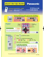
Summary of Contents for D-KR2SU

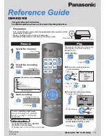
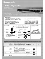
Page 1: ...DVD VIDEO RECORDER SERVICE MANUAL FILE NO 810 200413 D R2SU D R2SC D KR2SU DIGITAL VIDEO ...

Page 2: ...e mat soldering iron with ground wire etc to protect the laser diode from damage by static electricity And also the LSI and IC are same as above 1MW Ground conductive wrist strap for body Soldering iron with ground wire or ceramic type Conductive mat The ground resistance between the ground line and the ground is less than 10W LASER BEAM CAUTION LABEL When the power supply is being turned on you m...

Page 3: ...xists the fault must be located and corrected Repeat the above test with the DVD VIDEO RECORDER power plug reversed NEVER RETURN A DVD VIDEO RECORDER TO THE CUSTOMER WITHOUT TAKING NECESSARY CORRECTIVE ACTION READING SHOULD NOT EXCEED 0 3V The lightning flash with arrowhead symbol within an equilateral triangle is intended to alert the user to the presence of uninsulated dangerous voltage within t...

Page 4: ...m 4 4 1 Tuner Circuit Diagram 4 4 2 Timer Circuit Diagram 4 4 3 Audio Circuit Diagram 4 4 4 Video Circuit Diagram 5 PC BOARDS 5 1 Front Jack PC Board 5 2 Front L PC Board 5 3 Front R PC Board 5 4 Digital PC Board 5 5 Mother PC Board CONTENTS SECTION 1 GENERAL DESCRIPTIONS 1 OPERATING INSTRUCTIONS 1 Replacement of Mechanical Parts 1 1 Cabinet Replacement 1 1 1 Top Cover 1 1 2 Front Panel 1 1 3 Tray...

Page 5: ...SECTION 1 GENERAL DESCRIPTIONS 1 OPERATING INSTRUCTIONS Please refer to the owner s manual about the contents SECTION 1 GENERAL DESCRIPTIONS ...

Page 6: ...1 Location of Main Parts Fig 1 2 1 2 2 Location of PC Boards Fig 1 2 2 ZG45 FAN RAM1 RAM DRIVE EU05 Mother PC board EU01 Digital PC Board EU02 Power PC board EU03A Front R PC Board EU55 Front Jack PC Board EU03B Front L PC Board ...

Page 7: ...tic electricity and may easily damaged so do not forget to ground as required Many screws are used inside the unit To prevent the screws from missing or dropping etc always use a magnetized screwdriver in servicing Several kinds of screws are used and some of them need special cautions That is take care of the tapping screws securing molded parts and fine pitch screws used to secure metal parts If...

Page 8: ...crew 5 5 Remove two screws 6 6 Release four claws then remove the front panel 7 Fig 2 1 2 Flexible cable 2 Flexible cable 3 Tapes 1 Connector 4 Connector 4 Screws 6 Screw 5 Front panel 7 Claw Claw Claws 1 1 3 Tray Door 1 Remove the front R PC board and front L PC board Refer to item 1 2 4 2 Remove the spring 1 3 Remove the tray door 2 while slightly bending it Fig 2 1 3 Spring 1 Tray door 2 ...

Page 9: ...tion Panel Door 1 Open the operation panel door 1 2 Release two claws and unhinge the door 1 Fig 2 1 4 Front panel Hinge Claw Claw Hinge Operation panel door 1 Flexible cable 2 Flexible cable 2 Connector 3 Tapes 1 Tape 1 Acrylic board 5 Screws 6 Screws 4 RAM drive 7 Connector Claw Flexible cable 2 A A Remove the connector claw in the direction indicated by the arrows to release the flexible cable ...

Page 10: ...d the fan 4 Note After replacing the fan 4 attatch the tape 1 as it was 1 1 7 Rear Panel 1 Remove twelve screws 1 then remove the rear panel 2 Fig 2 1 7 Wire 5 Wire 5 Screws 3 Connector 2 Tape 1 Fan 4 Acrylic board Pass the wire 5 underneath the folded part Screws 1 Rear panel 2 Fig 2 1 6 ...

Page 11: ... drive Refer to 1 1 5 2 Disconnect two connectors 1 3 Peel off the tape 2 then disconnect the connector 3 4 Disconnect the connector 4 5 Remove four screws 5 and the digital PC board 6 Connector 4 Screws 5 Digital PC board 6 Connector 3 Tape 2 Connectors 1 Fig 2 1 8 ...

Page 12: ...item 1 1 5 2 Remove the rear panel Refer to item 1 1 7 3 Disconnect three connectors 1 4 Disconnect the flexible cable 2 5 Remove four screws 3 then remove the mother PC board 4 Fig 2 1 9 Screws 3 Mother PC board 4 Connectors 1 Flexible cable 2 Connector 1 ...

Page 13: ...s incorrectly replaced Replaceonlywiththesameorequivalenttype 1 Disconnect three connectors 1 2 Disconnect the connector 2 3 Remove the screw 3 four screws 4 and the power PC board 5 Fig 2 1 10 Connectors 1 Connector 1 Connector 2 Screw 3 Power PC board 5 Screws 4 ...

Page 14: ...2 3 Remove four screws 3 then remove the stay 4 4 Remove eight screws 5 and the screw 6 then remove the front R PC board 7 and front L PC board 8 5 Remove four screws 9 then remove the front Jack PC board 10 Fig 2 1 11 Screws 3 Screws 5 Screw 6 Screws 9 Stay 4 Front L PC board 8 Front R PC board 7 Flexible cable 1 Tape 2 Front Jack PC board 10 ...

Page 15: ...c and film capacitors of which capacitance are more than 10 pF None 5 or more B 0 1 C 0 25 D 0 5 F 1 G 2 2 Ceramic plastic and film capacitors of which capacitance are 10 pF or less None more than 5 pF B 0 1 pF C 0 25 pF 3 Electrolytic Trimmer Tolerance is not described Temperature characteristic None SL Ceramic capacitor For others temperature characteristics are described For capacitors of 0 01 ...

Page 16: ...forms for CD DVD and RF shown in the circuit diagrams are obtained when a test disc is played back All voltage values except the waveforms are expressed in DC and measured by a digital voltmeter 1 6 Others The parts indicated with NC or KETU etc are not used in the circuits of this model Eg 4 Eg 5 Fig 3 1 4 Fig 3 1 5 Type name 10m Type Tolerance ...

Page 17: ...N V_GND RXD R T TXD T R RTS T R CTS R T EVER6V GND EVER6V GND ON OFF15 3V GND ON OFF37V GND A_GND TPO TPO PowerGood CPU5V GND ON OFF5V GND ON OFF3 0V GND A GND GND GND TPI TPI TpAon TpBop TpBon CN506 CNZ01 GND GND DGND TpAop CTS2 SPICK PB LRCK PB DATA PB BCK CN902 REC_DATA CR OUT CB OUT V GND CY OUT V GND Y OUT V GND CV OUT REC_LRCK GND GND REC_BCK B B TPO GND TXD T E RTS T E CTS E T CN706 C IN GN...

Page 18: ...CPU uPD72893 1394 AV LINK DV uPD64011B 3D Y C_DNR ADC Decoder OSC 27MHz Audio AD Converter AK5365 Audio D A Converter PCM1751 NJM2115 16Mbit SDRAM 12 288MHz 16Mbit SDRAM 256Mbit DDR SDRAM X4 64kbit EEPROM PLL 64Mbit FLASH ROM OUT_1 OUT_1 IN_3 IN_2 IN_1 VHF UHF Timer CPU uPD784225Y FL_Driver BU2879AK 24 576MHz 24 576MHz 4 0MHz S in S in S in C_Video in C_Video in C_Video in Audio in L R Audio in L ...

Page 19: ...10 1 3 4 A B C D E G 2 5 6 7 8 9 F Fig 3 4 1 4 CIRCUIT DIAGRAMS 4 1 Power Supply Circuit Diagram ...

Page 20: ...1 3 4 A B C D E G 2 5 F 4 2 Front Circuit Diagram 4 2 1 Front Jack Circuit Diagram Fig 3 4 2 ...

Page 21: ...1 3 4 A B C D E G 2 5 F 4 2 2 Front L Circuit Diagram Fig 3 4 3 ...

Page 22: ...10 1 3 4 A B C D E G 2 5 6 7 8 9 F Fig 3 4 4 4 2 3 Front R Circuit Diagram ...

Page 23: ...Fig 3 4 5 4 3 Digital Circuit Diagram 4 3 1 Digital 1 Circuit Diagram ...

Page 24: ...4 3 Digital Circuit Diagram 4 3 1 Digital 1 Circuit Diagram ...

Page 25: ......

Page 26: ......

Page 27: ......

Page 28: ......

Page 29: ......

Page 30: ......

Page 31: ...Fig 3 4 5 ...

Page 32: ...Fig 3 4 6 4 3 2 Digital 2 Circuit Diagram ...

Page 33: ...4 3 2 Digital 2 Circuit Diagram ...

Page 34: ......

Page 35: ......

Page 36: ......

Page 37: ......

Page 38: ...Fig 3 4 6 ...

Page 39: ...10 1 3 4 A B C D E G 2 5 6 7 8 9 F Fig 3 4 7 4 4 Mother Circuit Diagram 4 4 1 Tuner Circuit Diagram ...

Page 40: ...10 1 3 4 A B C D E G 2 5 6 7 8 9 F 4 4 2 Timer Circuit Diagram Fig 3 4 8 ...

Page 41: ...10 1 3 4 A B C D E G 2 5 6 7 8 9 F 4 4 3 Audio Circuit Diagram Fig 3 4 9 ...

Page 42: ...10 1 3 4 A B C D E G 2 5 6 7 8 9 F 4 4 4 Video Circuit Diagram Fig 3 4 10 ...

Page 43: ... BOARDS 5 1 Front Jack PC Board 5 2 Front L PC Board Fig 3 5 1 EU55 Front Jack PC Broad Top side Fig 3 5 2 EU55 Front Jack PC Broad Bottom side Fig 3 5 3 EU03B Front L PC Broad Top side Fig 3 5 4 EU03B Front L PC Broad Bottom side ...

Page 44: ...10 1 3 4 A B C D E G 2 5 6 7 8 9 F 5 3 Front R PC Board Fig 3 5 5 EU03A Front R PC Broad Top side Fig 3 5 6 EU03A Front R PC Broad Bottom side ...

Page 45: ...06 C307 C308 C309 C311 C312 C313 C314 C315 C317 C318 C319 C320 C321 C322 C323 C324 C325 C326 C327 C328 C329 C330 C331 C333 C335 C337 C338 C339 C340 C341 C342 C344 C345 C346 C347 C350 C353 C354 C355 C356 C357 C358 C361 C362 C364 C365 C367 C368 C369 C370 C371 C372 C373 C374 C375 C376 C377 C380 C381 C382 C383 C384 C385 C387 C388 C389 C390 C391 C392 C393 C396 C507 C508 C511 C512 C515 C516 C519 C520 C5...

Page 46: ...JP223 JP224 JP225 JP226 JP227 JP228 JP229 JP230 JP231 JP232 JP233 JP234 JP235 JP236 JP237 JP238 JP239 JP240 JP241 JP242 JP243 JP244 JP245 JP246 JP247 JP248 JP249 JP250 JP251 JP252 JP253 JP254 JP255 JP256 JP257 JP258 JP259 JP260 JP261 JP262 JP263 JP264 JP265 JP266 JP267 JP268 JP269 JP270 JP271 JP272 JP273 JP274 JP275 JP276 JP277 JP278 JP279 JP280 JP281 JP282 JP283 JP284 JP285JP286 JP287 JP288 JP289...

Page 47: ...B01 ICW01 ICX01 ICX10 ICX31 KB01 L701 L702 L703 L704 L705 L903 LA03 LA04 LA05 LA06 LA07 LA08 LA09 LA10 LA11 LB11 MB02 Q700 Q701 Q901 Q902 Q903 Q904 QA01 QA02 QA03 QB05 QB06 QB07 QB08 QB10 QW02 QW03 QW04 QX01 QX06 QX08 QX09 QX11 QX31 QX32 R700 R701 R702 R704 R705 R707 R708 R714 R715 R732 R736 R738 R750 R764 R765 R770 R773 R774 R775 R776 R777 R778 R779 R780 R781 R782 R790 R900 R901 R902 R903 R904 R9...

Page 48: ...ocessing be sure to include the model number and description ABBREVIATIONS 1 Integrated Circuit IC 2 Capacitor Cap Capacitance Tolerance for Nominal Capacitance more than 10pF P 100 0 Symbol Tolerance B 0 1 C 0 25 D 0 5 F 1 G 2 J 5 K 10 M 20 N 30 V 20 10 W 100 10 U 75 10 Q 30 10 T 50 10 Symbol Tolerance X 40 20 Y 150 10 Z 80 20 Ex 10µF J 10µF 5 Symbol Tolerance pF B 0 1 C 0 25 D 0 5 F 1 G 2 Ex 10p...

Page 49: ...4 EXPLODED VIEWS 4 1 Packing Assembly Fig 4 4 1 ZF23 ZF01 ZF35 Note The shape of the packing material is sometimes different ZF10 ZF11 ZF12 ZF13 ...

Page 50: ...4 2 Chassis Assembly Fig 4 4 2 RAM1 ZG45 EU02 EU05 ZG20 W053 W058 W051 W051A EU01 EU55 ZG01 EU03B EU03A ...

Page 51: ...OP DR2UC English ZF11 P000398330 Owners Manual ST DR2UC English ZF12 P000398350 Owners Manual Q DR2UC English ZF13 P000398360 Owners Manual Q DR2U DR2SU Spanish ZF10 P000398380 Owners Manual OP DR2C DR2SC French ZF11 P000398370 Owners Manual ST DR2C DR2SC French ZF23 79088007 Power Cord ZF35 P000401300 IR Blaster RWS1000 0052L ZG01 P000402880 Front Panel D R2SU SC ZG20 P000402800 Cover Top ZG45 P0...

Page 52: ... Chip 1SS226 MISCELLANEOUS A100 P000391090 Display FL HNV 10SM28T S100 P000391050 Switch Tact LOCATION NUMBER PART NUMBER DESCRIPTION S102 P000391050 Switch Tact S103 P000391050 Switch Tact S104 P000391050 Switch Tact S105 P000391050 Switch Tact S106 P000391050 Switch Tact S107 P000391050 Switch Tact S108 P000391050 Switch Tact S109 P000391050 Switch Tact S110 P000391050 Switch Tact S111 P00039105...

Page 53: ...ems 2 at rear 1 in front 1 0Vp p 75W Sync signal negative Pin jack x 1 system 1 at rear Y 1 0Vp p 75W Sync signal negative C 0 286Vp p 75W 2 at rear 1 in front Mini DIN4 Pin x 3 systems Y 1 0Vp p 75W Sync signal negative C 0 286Vp p 75W 1 at rear Mini DIN4 Pin x 1 system Y output green 1 0Vp p 75W Sync signal negative Pin jack x 1 system PB PR output blue red 0 7Vp p 75W Pin jack x 1 system each 2...

Page 54: ...TOSHIBA CORPORATION 1 1 SHIBAURA 1 CHOME MINATO KU TOKYO 105 8001 JAPAN ...

Reviews: